
At present, modulation strategies suitable for switch mode power supply applications such as solar inverters and motor drives mainly include pulse width modulation (PWM) and space vector modulation (SVPWM). The theoretical basis of PWM technology is to digitally sample the modulated signal within one cycle into a pulse sequence equivalent to the amplitude change of the modulated signal. Due to its easy principle, simple control circuit, and simple modulation algorithm, it is widely used in uninterruptible power supply applications. SVPWM was originally applied in the drive control of frequency converters for AC motors. Its algorithm idea is completely different from PWM modulation technology, but starts from the three-phase overall vector combination to obtain a standard circular rotating magnetic flux, so that AC motors can achieve better performance at different switching frequencies. Compared with PWM technology, SVPWM has the characteristics of high voltage utilization rate and fast dynamic response speed. When SVPWM is used in multi-level solar inverter modulation, the modulation difficulty increases exponentially, so the SVPWM mode has certain limitations.
PWM modulation is based on digital sampling theory, which divides the modulation wave into many pulses and uses the principle of equal impulse to regulate the output voltage amplitude and frequency by changing the duty cycle within each switching cycle. The commonly used PWM modulation method in inverter systems is to use carrier wave and modulation wave stacking, generally using triangular wave as carrier wave and sine wave as modulation wave. By comparing the absolute values of the two, an impulse signal with a set pulse width variation can be obtained, which drives the switching state of the switching transistor. The PWM modulation algorithm can be divided into carrier co directional stacked modulation and carrier counter directional stacked modulation. Using different modulation strategies, the harmonic components of the output voltage of solar inverters also vary greatly. Due to the use of sine wave modulation in solar inverter systems, when the modulation signal is a sine wave, it can also be called sine pulse width modulation (SPWM).
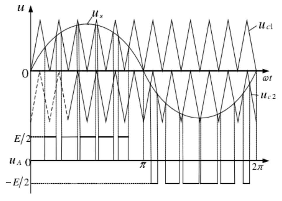
The principle of carrier co directional stacked modulation is shown in Figure 1, where carrier uc1 is in the upper layer and carrier uc2 is in the lower layer. The two have the same phase in the horizontal direction, but different amplitudes in the vertical direction. The modulated wave signal is us. When the amplitude of the modulation signal is positive, compare the modulation signal with the upper carrier uc1 and output a positive level pulse. When the amplitude of the modulation signal is negative, compared with the lower carrier uc2, a negative electric flat pulse is output. The positive and negative pulses are asymmetric within one cycle of the modulation signal, and the harmonic content of the carrier is relatively high.
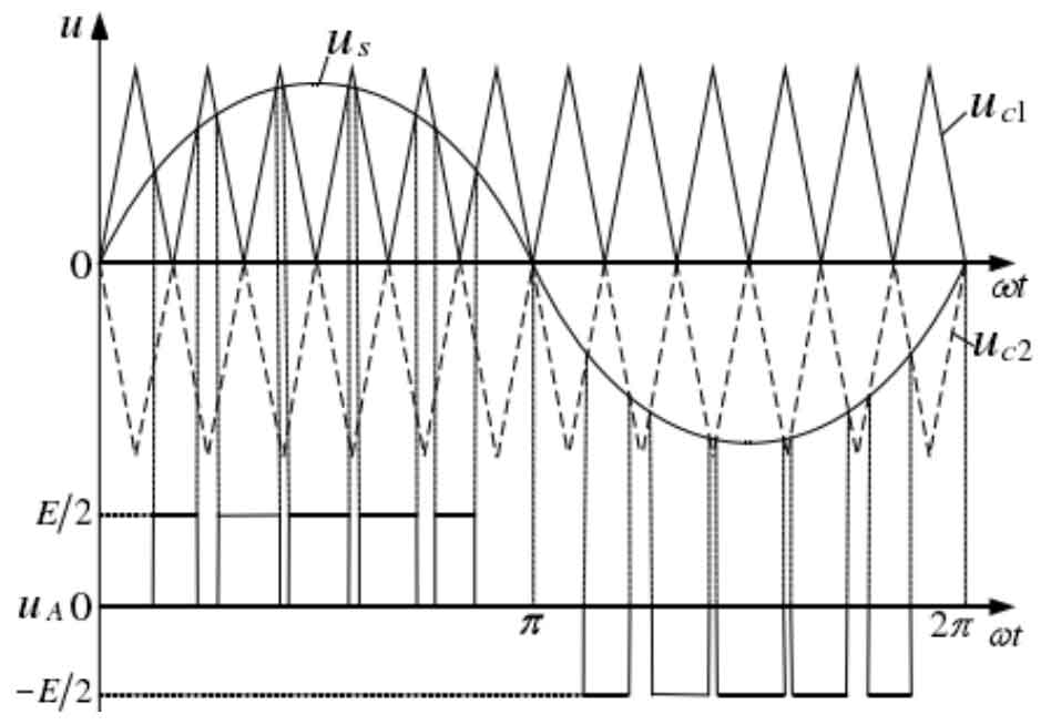
The principle of carrier heterodyne stacking modulation is shown in Figure 2. Similar to co directional carrier stacking, carrier uc1 is in the upper layer and carrier uc2 is in the lower layer. The two have the same phase in the horizontal direction and are symmetrical about the time axis in the vertical direction. The working process is also similar to the superposition of the same direction carrier wave, where the output pulse is symmetrical within positive and negative half cycles, and the harmonic content of the carrier wave is zero.
When using PWM strategy for modulation, the amplitude of the modulation signal is usually set to be smaller than the amplitude of the carrier signal to avoid over modulation. Meanwhile, PWM technology also has its shortcomings, which are the low utilization rate of DC voltage.
The phase voltages output by three-phase solar inverters are denoted as UA (t), UB (t), UC (t), representing A phase, B phase, and C phase, with equal amplitudes and a phase difference of 2 π/3, which can be expressed as:
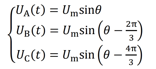
Among them θ = 2 π tfc is the angular momentum, and Um is the peak of the phase voltage. If using the ordinary civil power standard, which is a low-voltage power grid standard with a line voltage effective value of 380 V, the fundamental frequency fc is taken as 50 Hz, the peak phase voltage Um is 311 V, and the effective phase voltage is 220 V.
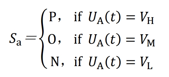
As mentioned earlier, the phase with the highest amplitude of phase voltage in the time domain is the H phase; The L-phase has the smallest amplitude of phase voltage; The phase voltage amplitude between the two is the M-phase. If VH represents the H-phase voltage, VM represents the M-phase voltage, and VL represents the L-phase voltage, it can be expressed as:
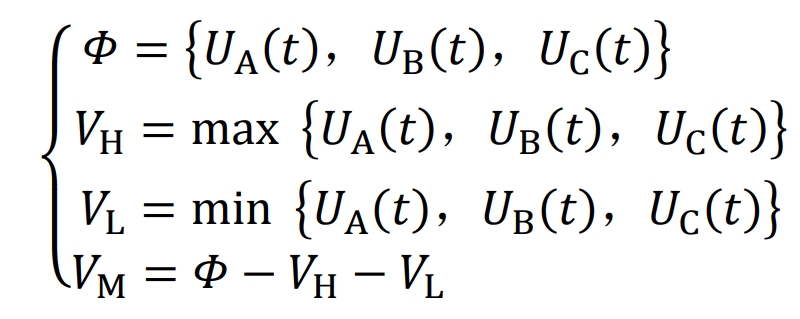
Where max represents the maximum value function, min represents the minimum value function, and its waveform is plotted according to the formula:
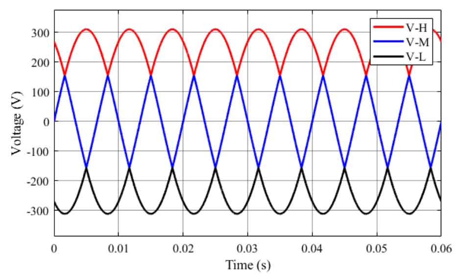
From Figure 3, it can be seen that the high, medium, and low three-phase can represent three adjustable levels, and the VH variation range is (Um/2~Um), the range of VM variation is (- Um/2~Um/2), and the range of VL variation is (- Um~Um/2). During the operation of a certain phase, it can be sequentially connected in the order of H → M → L → M → H to form a complete sine waveform. This is a modulation method based on phase voltage in the inverter system. At the same time, the front stage needs to provide three levels, high, medium, and low, for use by the rear stage.
For the modulation of the subsequent inverter circuit, the modulation process of phase A can be referred to. The switch state of the A-phase bridge arm is recorded as Sa, and when a high-level line is connected, it is recorded as state P. At this time, the switch tubes Q1a and Q2a are conducting; When connecting the intermediate level line, it is recorded as state O, and at this time, the switch tubes Q2a and Q3a are conducting; When connecting a low-level line, it is recorded as state N. At this time, the switch tubes Q3a and Q4a are conducting, which can be represented as:
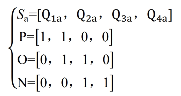
The switch tube of the A-phase bridge arm only needs to determine its switching state based on the amplitude of its modulation wave. When the amplitude of the A-phase modulation wave is maximum, the A-phase switch is adjusted to P state, when it is minimum, it is adjusted to N state, and when it is between the two, it is adjusted to O state. The relationship formula is:
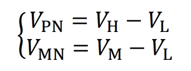
If the front-end circuit takes N as the reference point, it can only output two voltage values, so it needs to switch to the modulation mode of the line voltage. If the subsequent inverter circuit uses the L-phase voltage with the lowest amplitude as the reference voltage, let the line voltage of H-phase and L-phase at this time be VHL=VH-VL, and the line voltage of M-phase and L-phase be VML=VM-VL. If the H-phase is continuously connected to the high-level line P, the L-phase is directly connected to the low-level line N, and the M-phase is directly connected to the intermediate level line M, and the bus voltage is adjusted through the front-end circuit to make VPN=VHL, that is, the bus voltage is provided to the H-phase and L-phase of the back-end solar inverter to generate line voltage VHL. At the same time, adjust the intermediate level line M to make VMN=VML, that is, the midpoint voltage is provided to the intermediate phase M and low phase L of the subsequent inverter circuit to generate line voltage VML, and the line voltage of the subsequent inverter circuit meets the regular three-phase sine line voltage. By utilizing the switching action of the front stage to reduce the operating frequency of the rear stage switch, the voltage of the bus and midpoint is equal to the voltage of the three-phase output line. The use of a cascade control strategy can significantly reduce the switching and magnetic losses of the rear stage solar inverter.
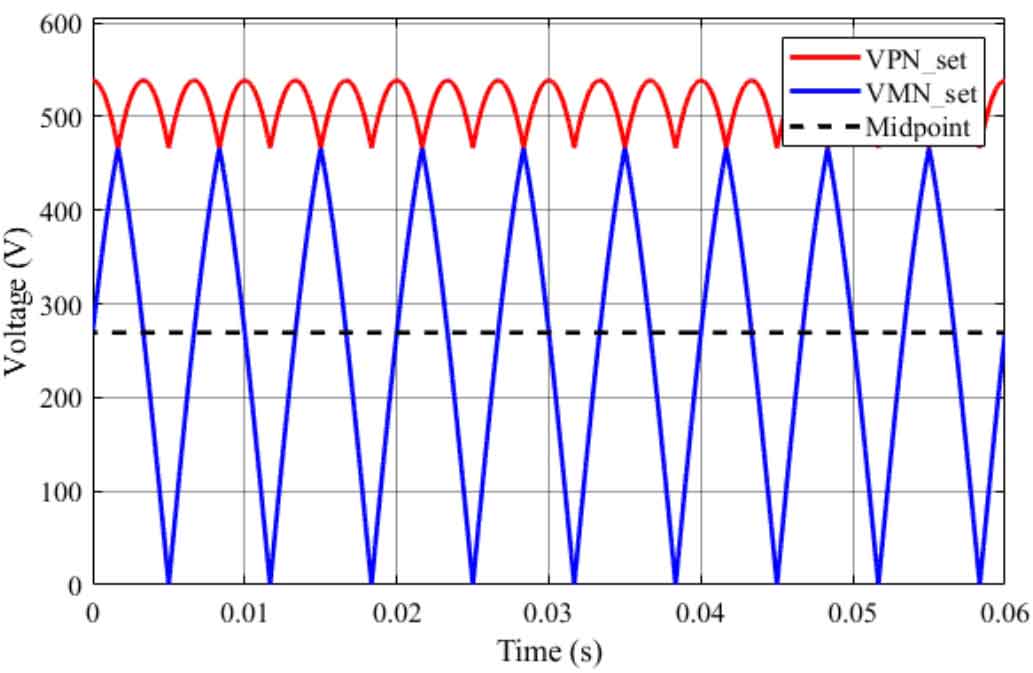
The maximum value of the bus voltage VPN is √ 3Um, which is 538.7 V, and the minimum value is 3Um/2, which is 466.5 V. The traditional NPC type solar inverter requires the bus voltage to be at least the peak to peak value of the modulation wave. Therefore, it can be seen that the modulation method proposed in this article will effectively reduce the bus voltage demand, thereby reducing the withstand voltage requirements of each phase bridge arm switching tube. For the solar inverter proposed in this article, due to circuit structure limitations, the single DC power supply voltage cannot exceed the minimum value of the bus voltage, and the sum of the two DC power supply voltages cannot be lower than the maximum value of the bus voltage. Therefore, the DC power supply voltage range is:
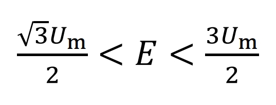
Therefore, when the peak output voltage of the three-phase is 311 V, the allowable fluctuation range of a single DC power supply voltage is 269 V to 466.5 V, and the maximum and minimum voltage input values are close to 1.8, which meets the design requirements for input voltage fluctuation of solar photovoltaic inverters.
When adjusting the midpoint voltage on the upper layer of the dotted line, i.e. VMN>Um √ 3/2, the voltage of phase M is positive, and the midpoint potential needs to output current. The front-end circuit uses a forward buck converter to adjust the midpoint voltage. When adjusting the lower midpoint voltage of the dotted line, i.e. VMN ≤ Um √ 3/2, the M-phase voltage is negative, and the midpoint potential needs to absorb current. Therefore, the front-end voltage regulation circuit needs to use a negative buck converter to absorb current and adjust the midpoint voltage. From the above working process, it can be seen that under ideal conditions, the voltage change before and after the IGBT switch in the rear stage solar inverter is 0, and each phase only needs to be switched four times in a sine cycle. The rear stage solar inverter can output three-phase sine voltage using only the bus DC voltage. This indicates that the inverter system proposed in this article can not only significantly reduce the pre – and post switching voltage of the solar inverter, but also reduce the switching frequency of the solar inverter, which will greatly improve its inverter efficiency.
The bus voltage and midpoint voltage adopt the traditional PWM modulation strategy, and the modulation signals of the bus voltage and midpoint voltage are compared with the carrier signal to output PWM pulse signals, controlling the corresponding switch operation. Its control strategy adopts PI control, which only needs to form a PI coefficient feedback from the modulation wave and output voltage error to the PI control processor to achieve real-time closed-loop control of bus voltage VPN and midpoint voltage VMN. This will help improve the dynamic response performance of the solar inverter system and ensure high-quality voltage waveform output.
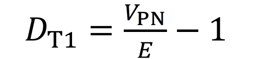
According to the formula, the duty cycle relationship of T1 can be obtained as follows:
Set the switching frequency to 15 kHz and the system sampling time to 0 2 us, set the maximum counter value to 333. The modulation signal of switch T1 after PI compensation is:
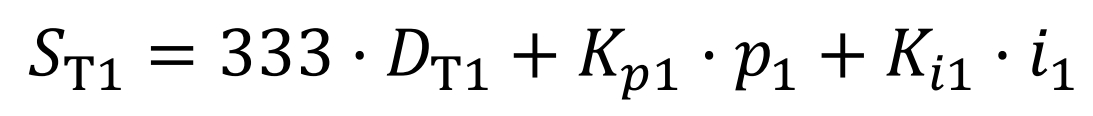
Where Kp1 is the proportional coefficient; P1 is the deviation between the set bus voltage at the current time and the actual output bus voltage; Ki1 is the integration coefficient; I1 is the integral of the current bus deviation voltage. If the value of the counter is less than the modulation signal, T1 conducts; otherwise, it turns off. The PI parameter will promptly adjust the duty cycle of T1 to achieve the same voltage output as the set voltage waveform. The midpoint voltage modulation method is similar to the above process.