
Solar inverters mainly achieve two functions: obtaining electrical energy from solar panels and making the output current of solar inverters in phase with the grid voltage.The following will be a certain modeling and simulation of the technologies related to these two functions.Among them, obtaining electrical energy from solar panels will involve maximum power point tracking technology, because the power of solar panels will constantly change with the intensity of light and temperature, so the power obtained by solar inverters from solar panels is also constantly changing (light intensity is proportional to current, and temperature is inversely proportional to voltage).Making the output current of solar inverters in phase with the grid voltage will involve the study of PI control loop.
1. Modeling of solar cells
Use MATLAB/SIMULINK to model and simulate solar cells.Before studying the MPPT system, first study the mathematical model of solar cells.Figure 1 shows the equivalent circuit model of solar cells.
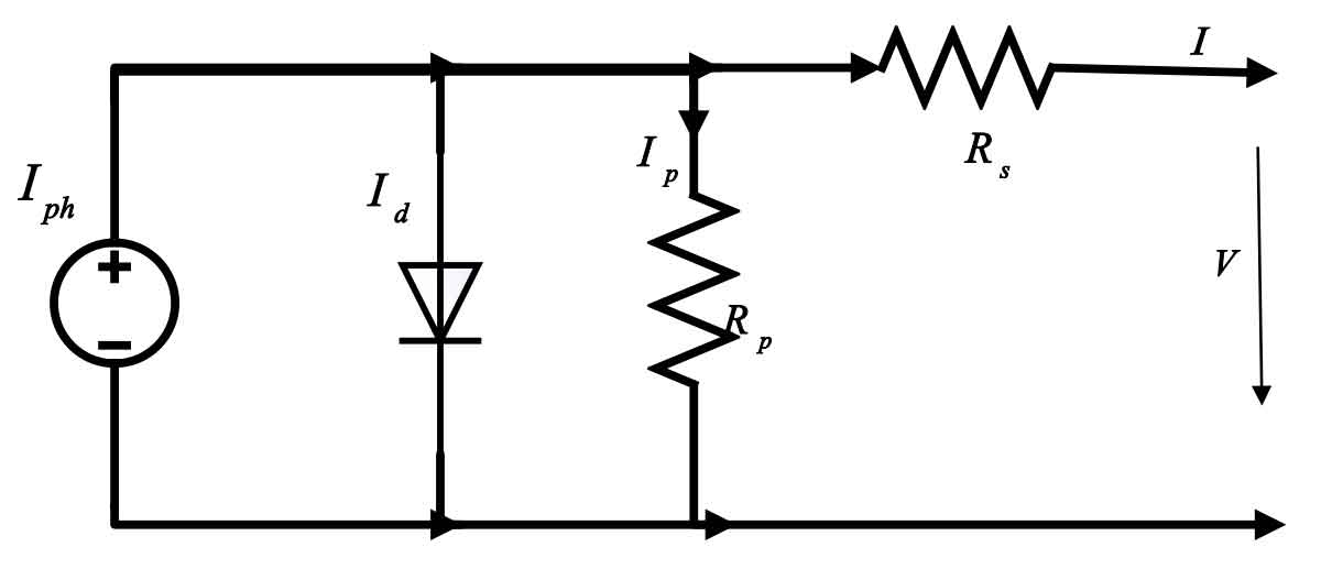
According to the current and voltage flow direction shown in Figure 1, the corresponding relationship between output current and output voltage can be obtained:
Where, Iph – photocurrent of solar cell, A;
Isa – reverse saturation current of diode, A;
q – electronic charge, 19 1.6 x10^-19 C;
V—output voltage, V;
I – output current, A;
Rs—equivalent resistance in series, Ω;
A – fitting constant, 1 ≤ A ≤ 2, when the solar output is high voltage, it is equal to 1, and when the output is low voltage, it is equal to 2;
K – Boltzmann constant, 1.38 X10^-23 / J K;
T—absolute temperature of solar cell, K;
Rp – parallel equivalent resistance, Ω.
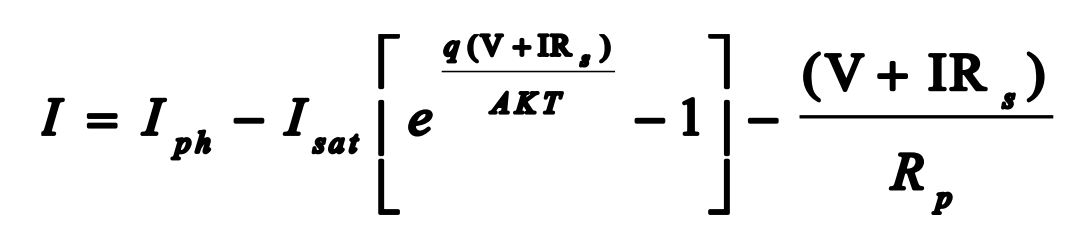
Now we make the following approximation to the above mathematical model:
(1) Since Rp is usually relatively large, the current passing through it is much smaller than the photocurrent and can be neglected;
(2) Since Rs is much smaller than the forward conduction resistance of the diode, it is assumed that Iph = Isc, where Isc
It represents the photovoltaic short circuit current, and the simplified formula is:
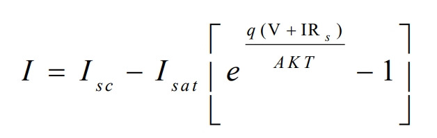
The voltage and current of the solar cell in the open circuit state (I=0, V=Voc) and at the maximum power point (I=Im, V=Vm) are respectively simplified by introducing them into the formula:
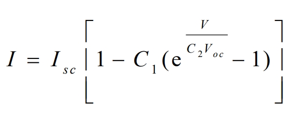
Among them,
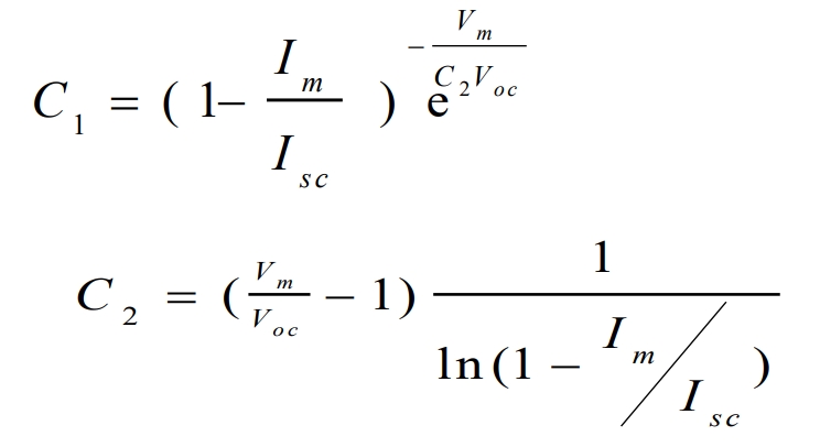
When the battery parameters Isc, Im, Voc, Vm are known, the values of C1 and C2 can be calculated, and then they can be inserted into the formula to obtain the I-V characteristic curve of the photovoltaic cell.
When the light intensity or temperature changes, the mathematical model of the solar cell needs to be corrected.Referring to the equivalent model of solar diode (Figure 1), we can obtain any point (I, V) on the I-V characteristic curve under new sunlight intensity and new cell temperature:
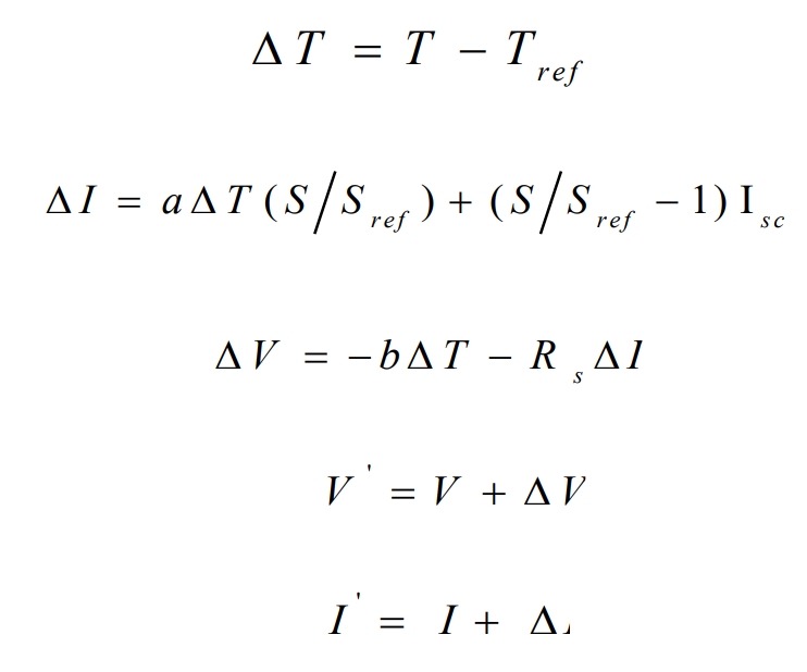
Wherein, Tref–reference battery temperature, 25℃;
Sref – refers to the sunshine intensity, 21000/Wm;
a – current temperature coefficient under reference sunlight intensity, A/℃;
b—the voltage temperature coefficient under reference sunlight intensity, V/℃.
According to the above relationship between photovoltaic cells, a simulation model was established in Matlab/Simulink as shown in Figure 2. This article selected Kyocera’s KD245GH-4YB, which has the following parameters when the light intensity is 11,000/Wm and the ambient temperature is 25℃: open circuit voltage Voc is 36.9V, short circuit current Isc is 8.91A, maximum power point corresponds to voltage 29.8V, corresponds to current 8.23A, maximum power Pm is 245W.

Then, the I-V characteristic curve of the battery model was compared with the actual measured value, as shown in Figure 3.
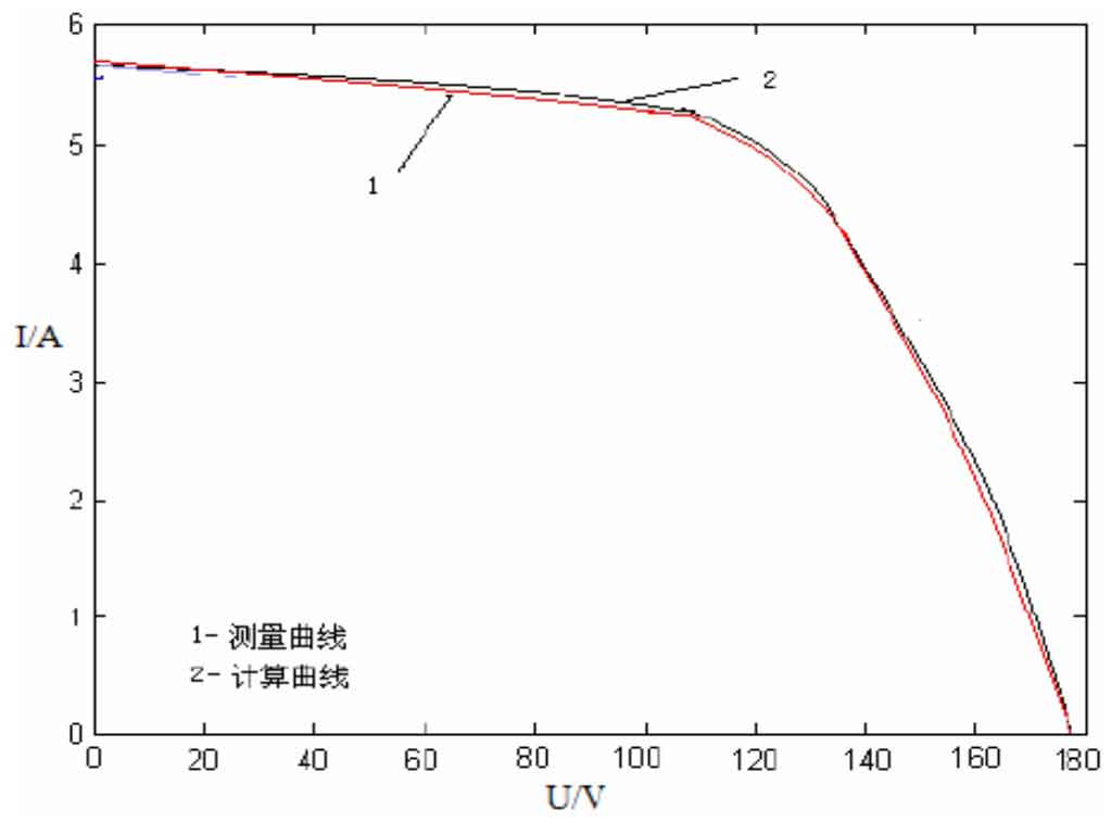
Among them, curve 1 is the measured volt-ampere characteristic curve, and curve 2 is the calculated curve of the model.From the figure, it can be seen that the calculated value of the model is almost the same as the actual value, which can meet the requirements of the photovoltaic power generation system.
2. Modeling Boost circuit, MPPT, and PWM
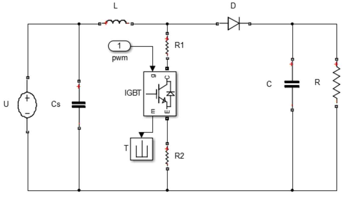
In DC-DC circuits, Boost circuits are used for DC boosting, and their topology structure is shown in Figure 4.
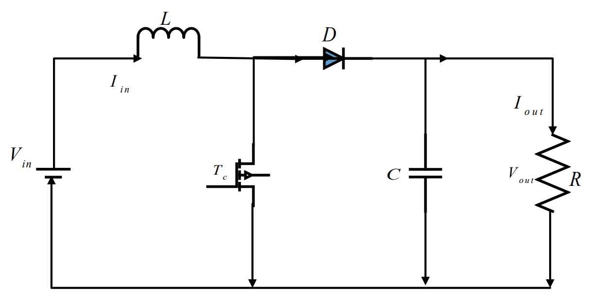
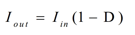
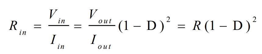
According to the principle of Boost circuit, the relationship between its input and output voltages can be known as follows:
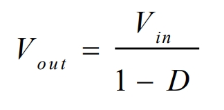
In the ideal state (no power loss):
Establish a Boost circuit simulation model, as shown in Figure 5:
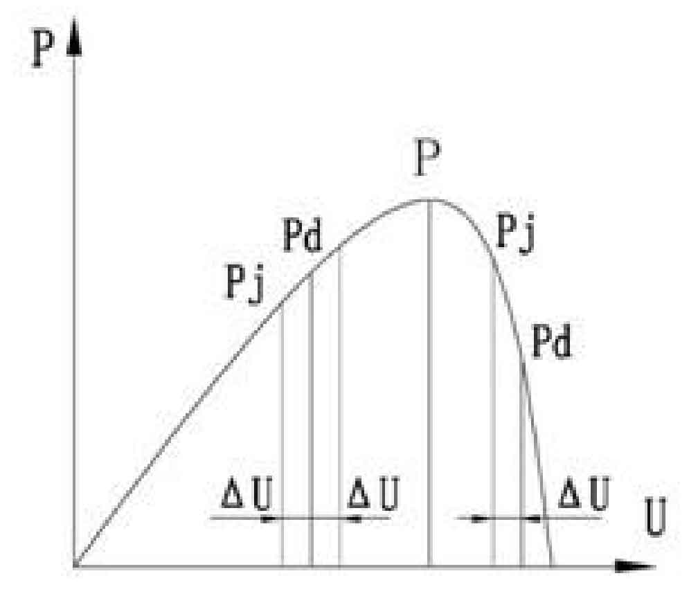
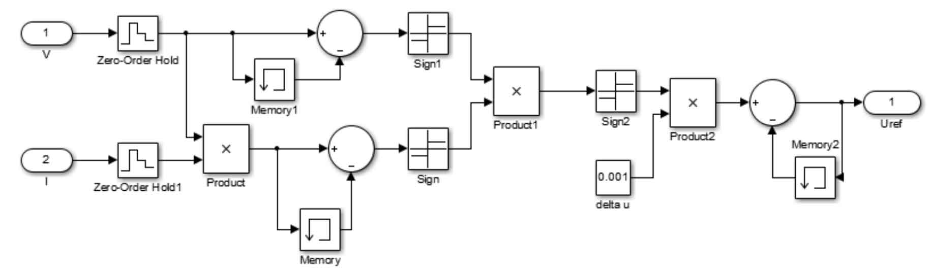
This article uses a fixed step disturbance observation method to model and simulate the MPPT of solar cells. The flowchart is shown in Figure 6-1, and Figure 6-2 shows the MPPT simulation model.The output of the model is the reference voltage Vref, where the sampling period of Zero-order Hold is the same as the sampling period of MPPT control.
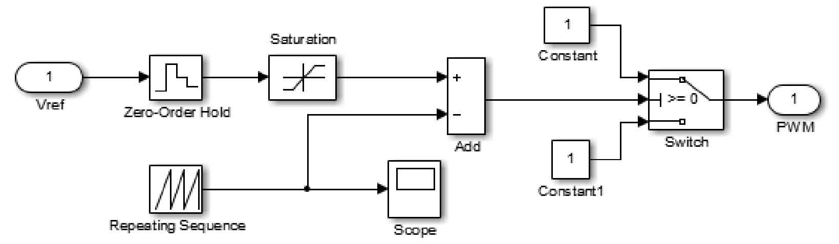
The modeling of the pulse width modulation (MPPT) module is shown in Figure 7. The on-off switching of the boost circuit switch device is controlled by the PWM signal generated by the comparison between Vref and the triangular wave.
3. Simulation analysis of MPPT system
By integrating the models of the first and second parts, a simulation model of the MPPT system can be obtained, as shown in Figure 8.
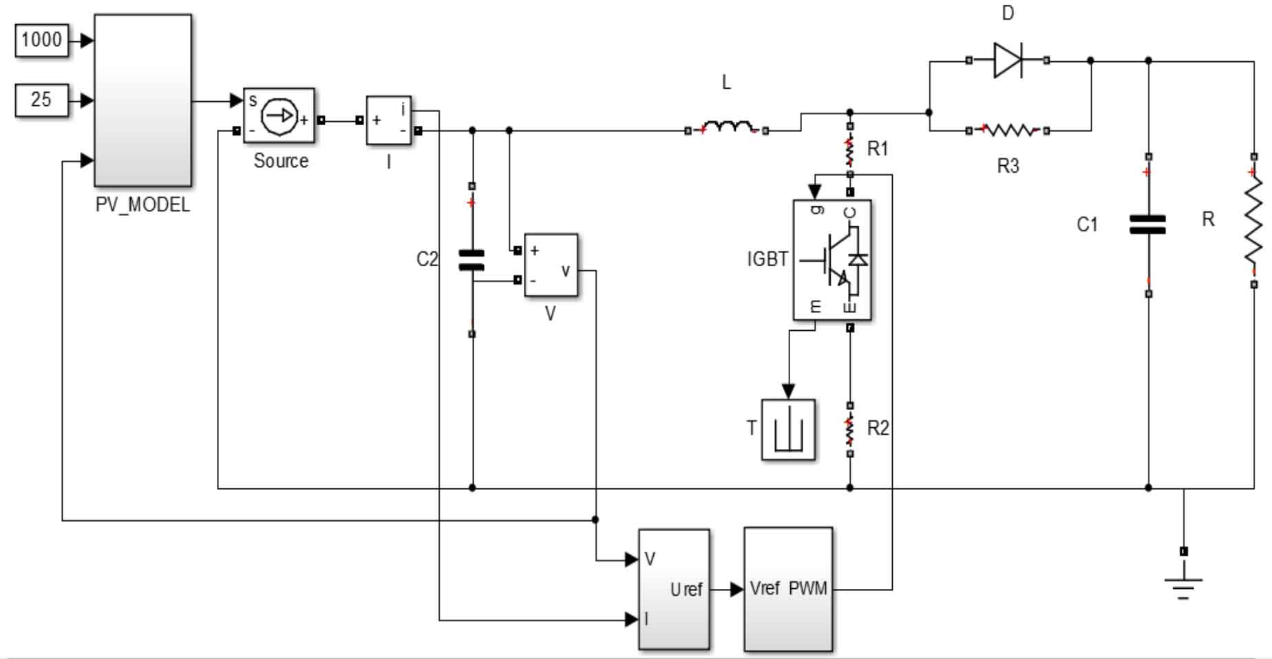
Figure 9 shows the MPPT simulation results obtained using Kyocera’s KD245 GH-4YB solar panel under standard conditions.
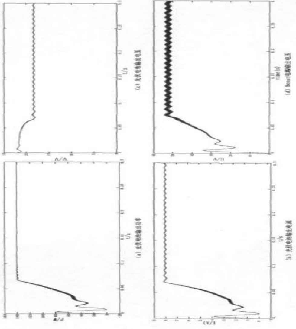
Figure 9(a) shows the output power of the photovoltaic cell, and the system reaches the maximum power point at 0.07 seconds;Figure 9(b) shows the output current of the photovoltaic cell;Figure 9(c) shows the output voltage of the photovoltaic cell;Figure 9(d) shows the output voltage of the Boost circuit, which is approximately 3 times higher after stabilization.
4. Experiment of single-phase photovoltaic inverter system
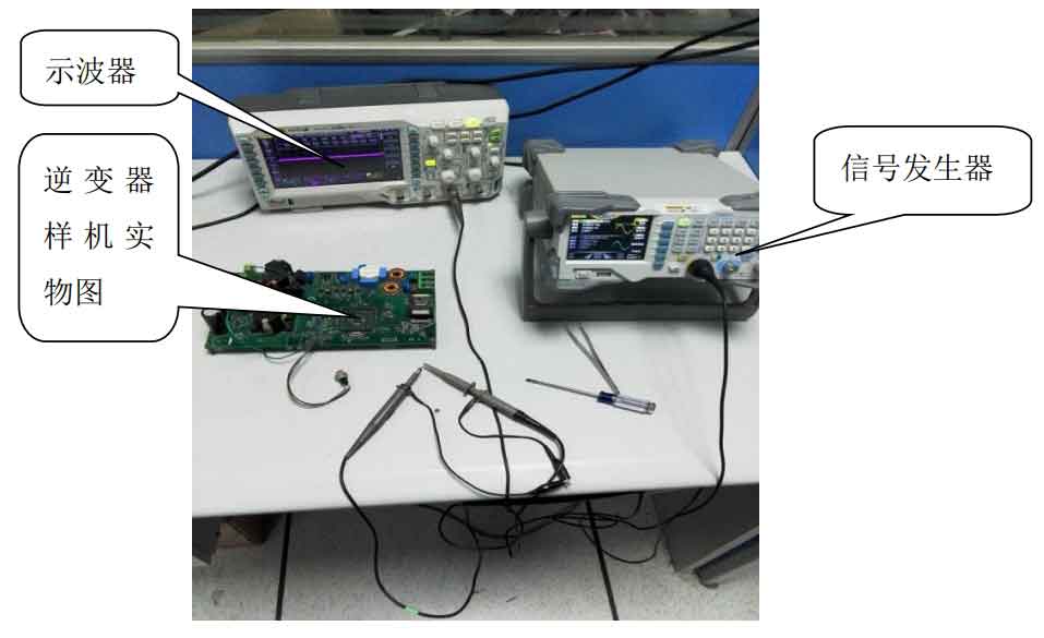
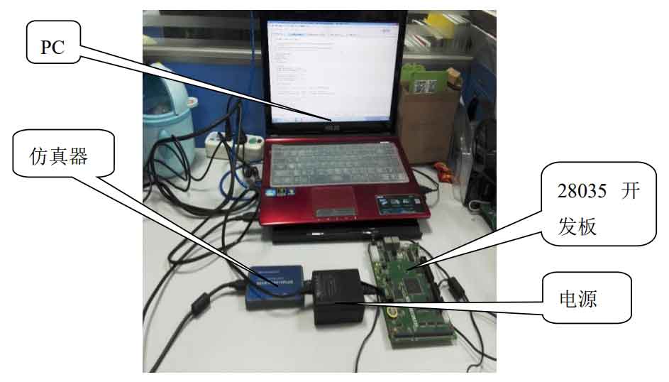
Figure 10 is a waveform diagram of a single-phase solar inverter. As shown in the figure, it mainly consists of experimental equipment such as a solar inverter prototype, an oscilloscope, and a waveform generator. Figure 11 is a program debugging diagram of a single-phase solar inverter, which mainly consists of PC, TMS320F28035 development board, XDS510 emulator, power supply, and other equipment.
4.1 Open-loop detection of solar inverters
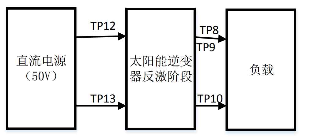
After connecting the experimental equipment, the next step is to test the solar inverter in the open-loop stage.The hardware settings of the solar inverter are described in Chapter 3, and the software configuration is described in Chapter 4.Rearrange the configuration of the DC power supply connected to the input terminal of the solar inverter, and connect a 100-200 ohm resistor to the output terminal of the solar inverter.The connection point between the power supply and the load must be specifically emphasized as shown in Figure 12.When connecting, keep the high-voltage power supply disconnected, and do not turn it on unless specifically indicated.
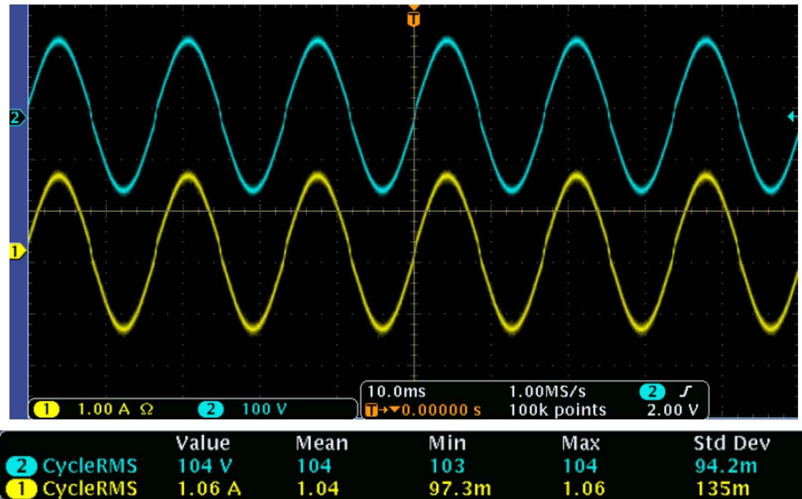
According to the software model of solar inverter described in Chapter 4, the first-level solar inverter voltage and current detection is constructed on the oscilloscope as shown in Figure 13.
4.2 Testing of photovoltaic inverter systems with maximum power point tracking systems
Solar panels and panel simulators are used at the input of the flyback module. Figure 14 shows the hardware configuration of a two-stage connection. The typical input of a solar panel simulator is:
Open circuit voltage: 40V, short circuit current: 5.2A, maximum power point voltage: 30V, maximum power point current: 4A.
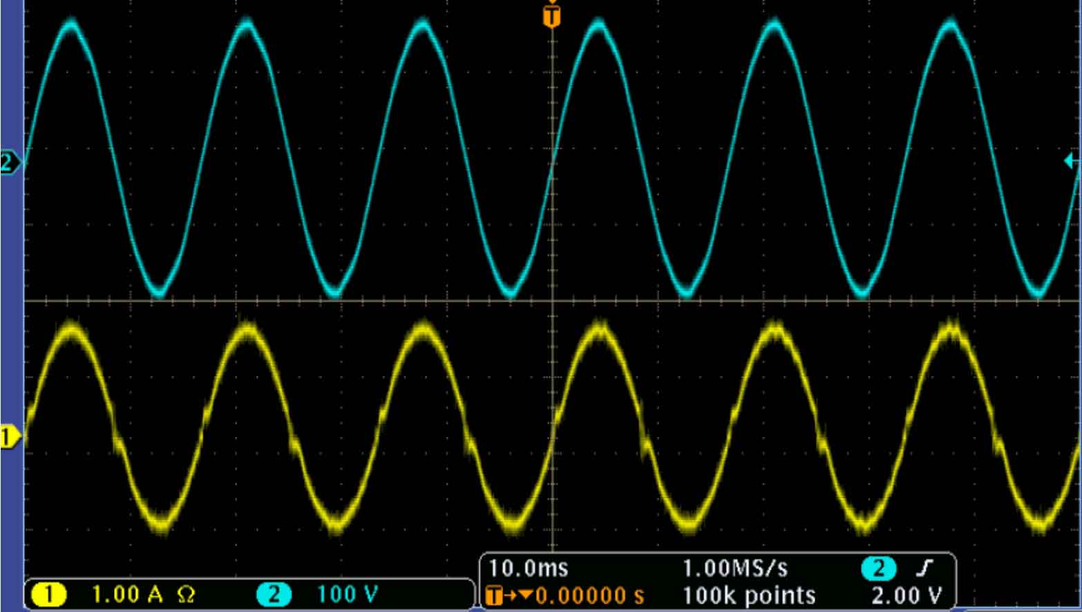
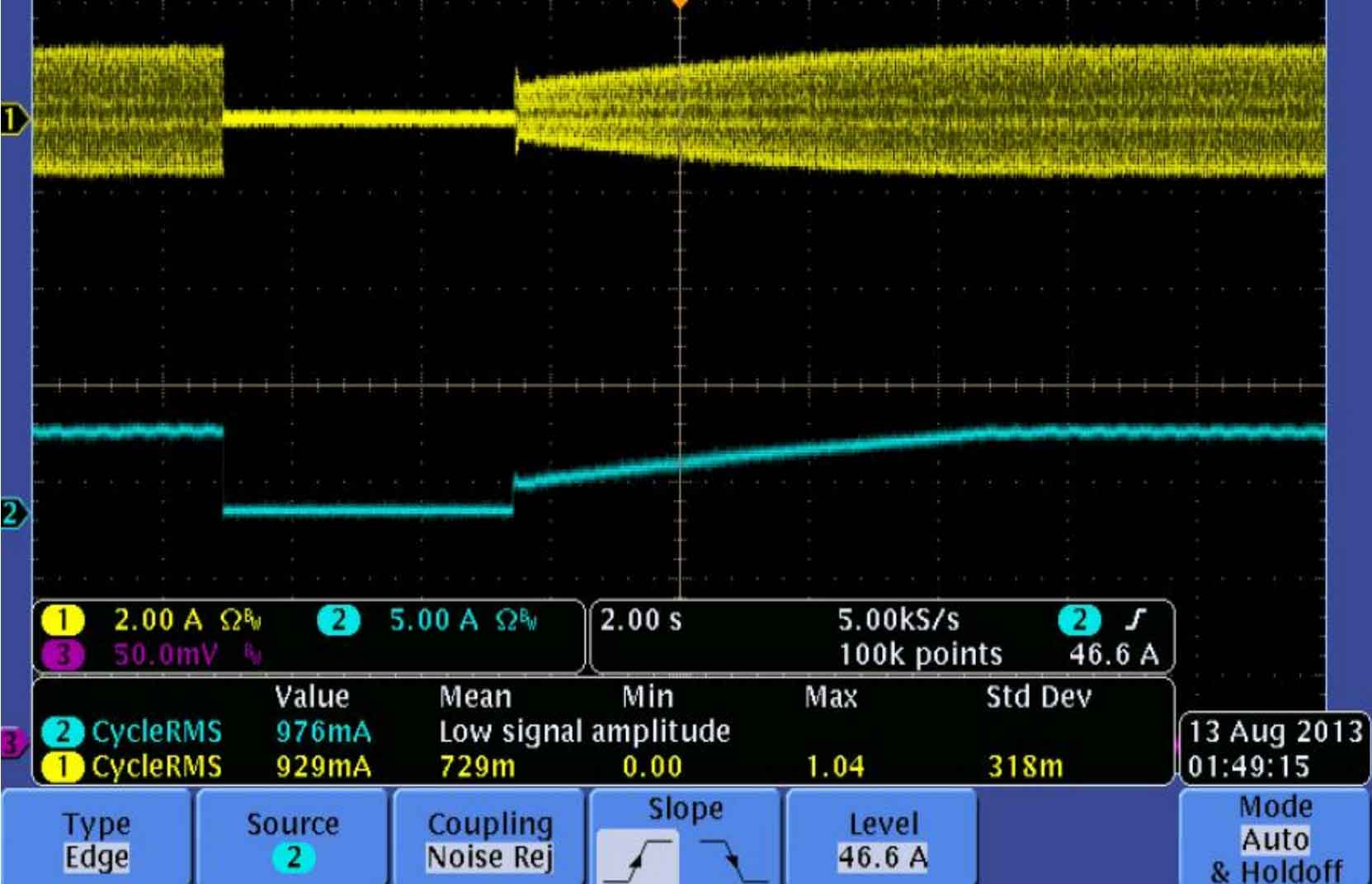
Based on the input data of the above-mentioned simulator, combined with the introduction of the hardware and software structure of solar inverters, the detection range of grid-connected detection voltage and current waveforms can be obtained, as shown in Figure 15.The current of the solar panel slowly increases to the current of the maximum power point, and using the solar panel simulator, different shadow states can be tested and intermediate states can be evaluated. Figure 16 shows the start and stop sequence of the capture range of the photovoltaic inverter.
4.3 Experimental waveform and analysis of the main circuit
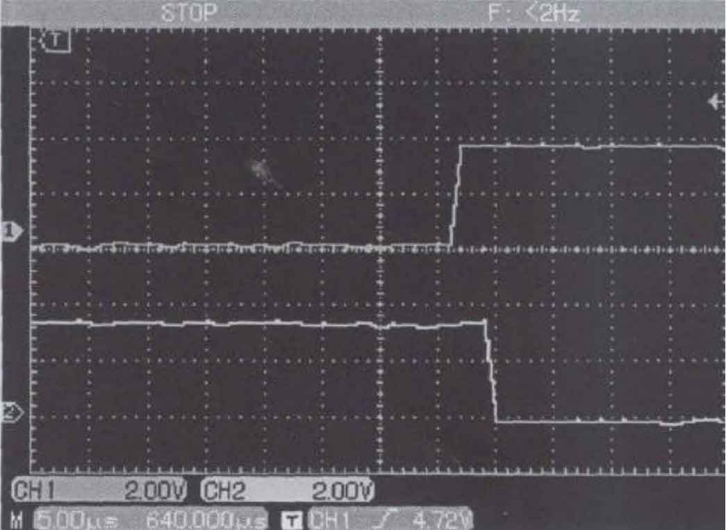
Measure the pins 51, 54, and 56 of the TMS320F28035 chip to output high levels of PWM3, PWM2, and PWM1;the pins 50, 53, and 55 output low levels of PWM3, PWM2, and PWM1.As shown in Figure 17, the period of the PWM waveform emitted from the main chip TMS320F28035 is approximately 560us.Among them, PWM1 and PWM2 are used to drive the interleaved flyback circuit;PWM3 is used to drive the full bridge circuit.
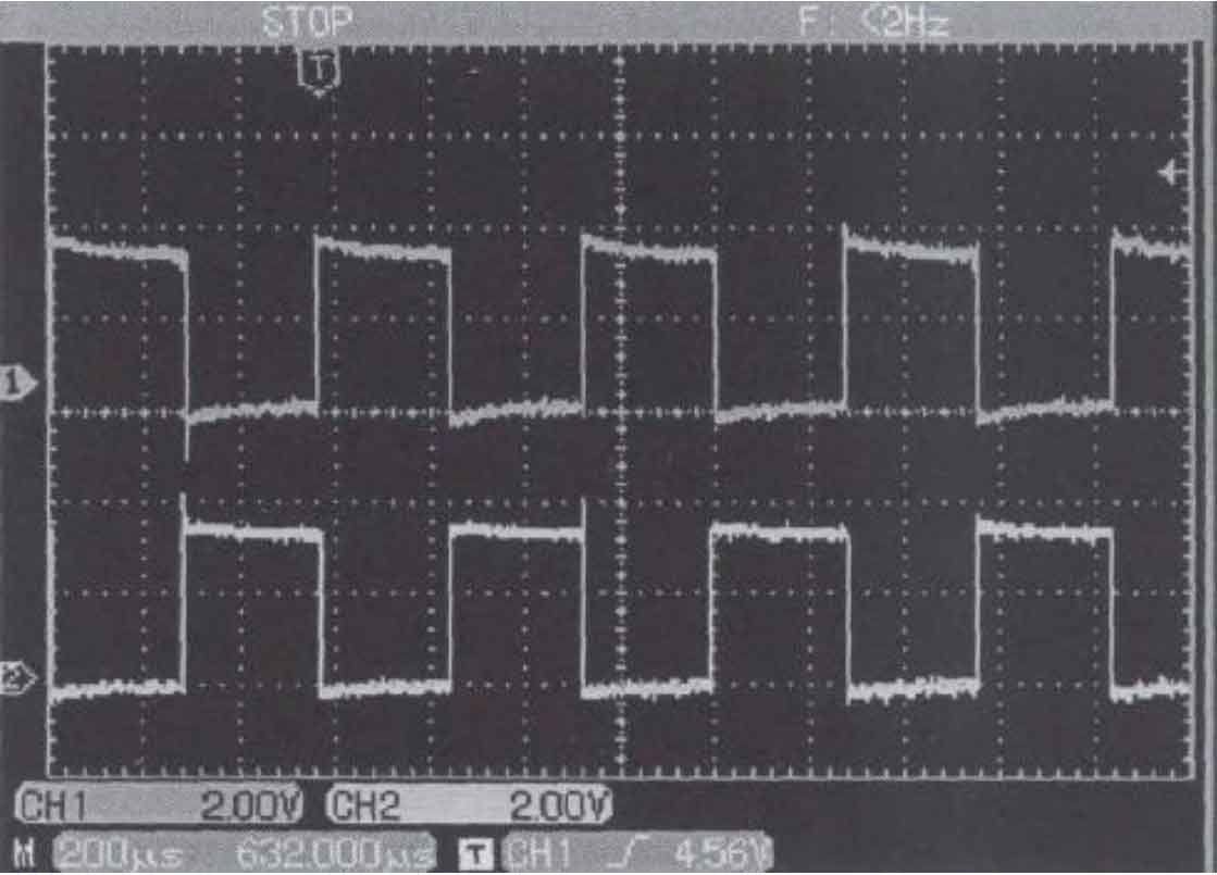
Figure 18 shows the enlarged waveform of Figure 17, with a dead time of approximately 5.6us.
Modulating the input DC voltage to 20V, we can obtain the AC output waveform shown in Figure 19, with a peak value of 20V. The waveform shape is the same as the PWM waveform, but the peak values are different.
5. Summary
This chapter mainly uses MATLAB/SIMULINK to systematically model and simulate the key components of the photovoltaic inverter system, such as solar panels, Boost circuits, fixed step disturbance observation method, pulse width modulation (PWM), and PI control. The modeling process of solar cells and Boost circuits is comprehensively and systematically derived: the mathematical relationship is derived from the simplified circuit diagram, and the mathematical model is established based on the corresponding mathematical relationship. The simulation analysis is carried out on the MPPT overall system model platform.The simulation results well meet the practical requirements, proving that this MPPT system has strong practicality and economy, and can be widely promoted.The experiment mainly conducts waveform experiments on the solar inverter prototype. The experiment proves that this PI system can achieve the function of phase synchronization between the output current of the solar inverter and the grid voltage, which has good application prospects.