
As a researcher in the field of renewable energy, I have always been fascinated by the potential of solar cells to address global energy challenges. Perovskite solar cells have emerged as a promising technology due to their high efficiency and low-cost fabrication potential. In this article, I will describe an innovative experiment focused on the full-solution preparation of inverted perovskite solar cells, designed to make this advanced topic accessible for educational purposes. The experiment utilizes simple spin-coating techniques to fabricate complete devices, eliminating the need for expensive vacuum equipment. This approach not only simplifies the process but also enhances safety and reproducibility, allowing students to gain hands-on experience with solar cell principles, fabrication, and characterization. Throughout this work, I will emphasize the importance of perovskite solar cells in the context of sustainable energy and provide detailed insights into the methodology, results, and educational implications.
The growing demand for clean energy sources has intensified research into solar technologies. Perovskite solar cells have garnered significant attention due to their rapid efficiency improvements, with current records exceeding 26% for lab-scale devices. These cells leverage the unique properties of perovskite materials, such as high absorption coefficients and tunable bandgaps, to convert sunlight into electricity efficiently. The inverted structure of perovskite solar cells, which I will focus on here, offers advantages like better stability and compatibility with flexible substrates. In this experiment, I aim to demonstrate how a full-solution method can be employed to fabricate these devices, making it feasible for undergraduate laboratories to explore this cutting-edge technology. By integrating concepts from materials science, chemistry, and physics, this experiment helps bridge the gap between theoretical knowledge and practical application in the field of perovskite solar cells.
To begin, let me outline the fundamental principles underlying perovskite solar cells. The operation of these devices is based on the photovoltaic effect, where light absorption generates electron-hole pairs that are separated and collected to produce electrical current. In an inverted perovskite solar cell, the typical structure consists of a transparent conductive oxide (e.g., ITO) as the anode, followed by a hole transport layer, the perovskite active layer, an electron transport layer, and a metal cathode. When light strikes the perovskite layer, photons are absorbed, creating excitons that dissociate into free carriers due to the built-in electric field at the interfaces. The holes are transported through the hole transport layer to the anode, while electrons move via the electron transport layer to the cathode, resulting in a current flow through an external circuit. The efficiency of a perovskite solar cell can be expressed using the following equation for power conversion efficiency (PCE):
$$ \text{PCE} = \frac{J_{\text{sc}} \times V_{\text{oc}} \times \text{FF}}{P_{\text{in}}} $$
where \( J_{\text{sc}} \) is the short-circuit current density, \( V_{\text{oc}} \) is the open-circuit voltage, FF is the fill factor, and \( P_{\text{in}} \) is the incident light power density. This formula is central to evaluating the performance of perovskite solar cells and will be used extensively in the analysis later. Additionally, the external quantum efficiency (EQE) is another critical parameter, defined as the ratio of collected electrons to incident photons at a given wavelength, and it relates to \( J_{\text{sc}} \) by:
$$ J_{\text{sc}} = q \int \text{EQE}(\lambda) \phi(\lambda) \, d\lambda $$
where \( q \) is the electron charge, \( \lambda \) is the wavelength, and \( \phi(\lambda) \) is the photon flux. Understanding these principles is essential for students to appreciate how material properties and device architecture influence the performance of perovskite solar cells.
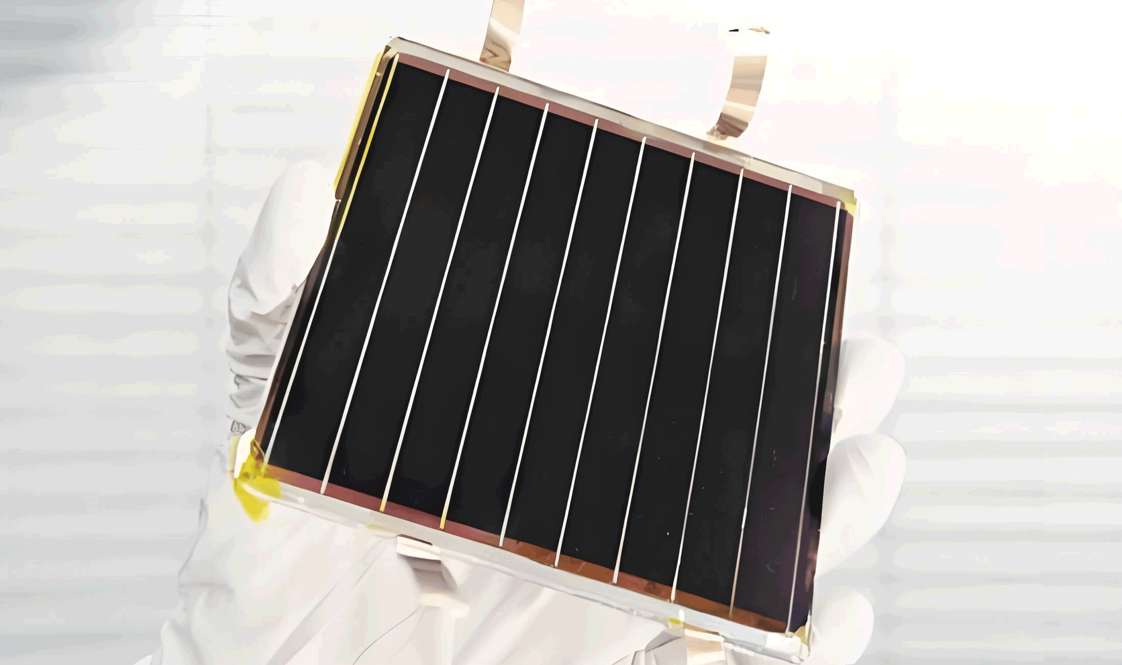
In the experimental setup, I employed a full-solution spin-coating method to fabricate inverted perovskite solar cells. This technique was chosen for its simplicity and cost-effectiveness, as it avoids the need for high-vacuum deposition systems. The materials used included lead iodide (PbI₂), methylammonium iodide (MAI), nickel oxide (NiOₓ) nanoparticles for the hole transport layer, phenethylammonium iodide (PEAI) for surface passivation, and an organic polymer (N2200) for the electron transport layer. Silver nanowires were used as the cathode electrode. All solvents, such as dimethylformamide (DMF) and chlorobenzene, were handled with care to ensure safety, especially given the toxicity of lead-based compounds. The step-by-step procedure involved cleaning the ITO substrates, depositing each layer by spin-coating, and thermal annealing to form the perovskite film. Two devices were prepared with different annealing temperatures (100°C and 120°C) to investigate the impact on film morphology and device performance. This comparative approach allows for a deeper understanding of how processing conditions affect the properties of perovskite solar cells.
The fabrication process began with the thorough cleaning of ITO glass substrates using sequential ultrasonication in detergent, deionized water, ethanol, acetone, and isopropanol. This was followed by oxygen plasma treatment to improve surface wettability. The hole transport layer was deposited by spin-coating a dispersion of NiOₓ nanoparticles in DMF at 2000 rpm for 50 seconds, then annealing at 140°C for 10 minutes. Next, the perovskite precursor solution was prepared by dissolving PbI₂, PbCl₂, and MAI in DMF with a molar ratio of 0.9:0.1:1, respectively, and filtered before use. This solution was spin-coated at 4000 rpm, with toluene added as an anti-solvent during spinning to induce crystallization. The films were annealed at either 100°C or 120°C for 10 minutes to form the perovskite layer. Subsequently, a PEAI passivation layer was applied by spin-coating from an isopropanol solution, followed by annealing. The electron transport layer was deposited using a solution of N2200 in chlorobenzene, and finally, the silver nanowire electrode was spin-coated and annealed. This comprehensive process highlights the versatility of the full-solution method for constructing perovskite solar cells.
To characterize the perovskite films and devices, I used various techniques, including scanning electron microscopy (SEM), X-ray diffraction (XRD), ultraviolet-visible (UV-Vis) spectroscopy, photoluminescence (PL), time-resolved photoluminescence (TRPL), current-density-voltage (J-V) measurements, and external quantum efficiency (EQE) analysis. The SEM images revealed differences in grain size and morphology between the two annealing conditions. For the film annealed at 100°C, the grains were densely packed with sizes ranging from 100 to 300 nm, whereas the 120°C annealed film showed larger grains (300–500 nm) but with more pronounced grain boundaries and voids. This structural variation is critical, as it influences charge carrier recombination and transport in perovskite solar cells. The XRD patterns confirmed the formation of the perovskite phase, with characteristic peaks at 14.11°, 28.44°, 31.89°, and 40.68° corresponding to the (110), (220), (310), and (330) planes of CH₃NH₃PbI₃. However, a small peak at 12.57° indicated the presence of residual PbI₂, which was more prominent in the 120°C annealed sample, suggesting partial decomposition at higher temperatures.
The optical properties of the perovskite films were assessed using UV-Vis absorption and photoluminescence spectroscopy. The UV-Vis spectra showed similar absorption edges for both samples, but the 120°C annealed film had slightly lower absorption in the 400–600 nm range, likely due to increased defect density. The PL spectra exhibited an emission peak at around 769 nm for both, but the intensity was lower for the 120°C sample, indicating higher non-radiative recombination. TRPL measurements further supported this, with carrier lifetimes of 109 ns and 212 ns for the 100°C and 120°C annealed films, respectively. The shorter lifetime in the 120°C sample implies enhanced charge carrier recombination, which can detrimentally affect the performance of perovskite solar cells. These findings underscore the importance of optimizing annealing conditions to achieve high-quality films for efficient perovskite solar cells.
The photovoltaic performance of the fabricated perovskite solar cells was evaluated through J-V measurements under simulated AM 1.5G illumination. The key parameters, including \( V_{\text{oc}} \), \( J_{\text{sc}} \), FF, and PCE, are summarized in the table below. The device annealed at 100°C (Device 1) exhibited a PCE of 16.83%, with a \( V_{\text{oc}} \) of 1.058 V, \( J_{\text{sc}} \) of 22.34 mA/cm², and FF of 71.19%. In contrast, the device annealed at 120°C (Device 2) showed a lower PCE of 15.70%, with reductions in all parameters: \( V_{\text{oc}} \) = 1.039 V, \( J_{\text{sc}} \) = 21.95 mA/cm², and FF = 68.84%. This decline in performance can be attributed to the increased defect density and carrier recombination in the 120°C annealed film, as evidenced by the characterization data. The EQE spectra further confirmed these results, with Device 1 demonstrating higher quantum efficiency across the visible spectrum, particularly in the 440–540 nm and 680–770 nm ranges. The integrated \( J_{\text{sc}} \) from EQE data matched well with the J-V measurements, validating the reliability of the results. These outcomes highlight the critical role of film quality in achieving high-efficiency perovskite solar cells.
| Device | Annealing Temperature (°C) | \( V_{\text{oc}} \) (V) | \( J_{\text{sc}} \) (mA/cm²) | FF (%) | PCE (%) |
|---|---|---|---|---|---|
| 1 | 100 | 1.058 | 22.34 | 71.19 | 16.83 |
| 2 | 120 | 1.039 | 21.95 | 68.84 | 15.70 |
In addition to the performance metrics, I analyzed the impact of material properties on device behavior using mathematical models. For instance, the diode equation can be applied to describe the J-V characteristics of perovskite solar cells:
$$ J = J_{\text{ph}} – J_0 \left( \exp\left(\frac{q(V + J R_s)}{n k T}\right) – 1 \right) – \frac{V + J R_s}{R_{\text{sh}}} $$
where \( J_{\text{ph}} \) is the photocurrent density, \( J_0 \) is the reverse saturation current, \( R_s \) is the series resistance, \( R_{\text{sh}} \) is the shunt resistance, \( n \) is the ideality factor, \( k \) is Boltzmann’s constant, and \( T \) is the temperature. By fitting this equation to the experimental data, students can extract parameters that reflect the quality of the perovskite solar cell, such as recombination losses and charge transport efficiency. For example, a higher \( R_s \) or lower \( R_{\text{sh}} \) often indicates issues like poor contacts or shunting paths, which were more evident in Device 2 due to its inferior film morphology. This analytical approach deepens the understanding of how material and processing variables influence the overall performance of perovskite solar cells.
The educational implementation of this experiment is designed to foster collaborative learning and critical thinking. Students work in groups of 3–4 over three sessions, each lasting 4 hours, to complete the fabrication and characterization. Pre-lab activities include reviewing the principles of perovskite solar cells and safety protocols, particularly for handling lead-based materials. During the lab, students prepare solutions, clean substrates, and assemble devices, followed by testing and data analysis. The use of Origin software for plotting J-V curves, EQE spectra, and other graphs helps develop data processing skills. Discussion questions prompt students to relate film properties to device performance, such as how grain size affects carrier lifetime in perovskite solar cells. Safety measures, like using fume hoods and personal protective equipment, are emphasized to minimize risks. This hands-on experience not only reinforces theoretical concepts but also prepares students for careers in renewable energy research, where perovskite solar cells are a key focus.
In conclusion, this innovative experiment demonstrates the feasibility of using full-solution methods to fabricate high-performance inverted perovskite solar cells in an educational setting. By simplifying the fabrication process and leveraging accessible characterization tools, it provides a comprehensive learning experience that integrates multiple disciplines. The results show that annealing temperature significantly affects film quality and device efficiency, with lower temperatures yielding better performance due to reduced defects and recombination. This insight is valuable for optimizing perovskite solar cells for real-world applications. As the demand for clean energy grows, experiments like this play a crucial role in training the next generation of scientists and engineers to advance solar technology. I believe that through such practical endeavors, students can gain a deeper appreciation for the complexities and potentials of perovskite solar cells, driving innovation in the field.
To further elaborate on the significance of this work, I would like to discuss some additional aspects of perovskite solar cells. For instance, the stability of these devices is a major research area, as perovskite materials can degrade under environmental factors like moisture, oxygen, and heat. In this experiment, the use of a passivation layer (PEAI) helps to mitigate some of these issues by reducing surface defects. The long-term stability of perovskite solar cells can be modeled using degradation kinetics, often expressed as:
$$ \frac{d[P]}{dt} = -k [P]^n $$
where [P] represents the concentration of the perovskite phase, \( k \) is the rate constant, and \( n \) is the reaction order. By incorporating such models into the curriculum, students can explore the durability of their fabricated devices, adding another layer of depth to the experiment. Moreover, the scalability of solution-processed perovskite solar cells is a key advantage for commercial adoption, and this experiment provides a foundation for understanding large-scale manufacturing techniques like slot-die coating or inkjet printing. Overall, the full-solution approach for perovskite solar cells not only makes the technology accessible for education but also aligns with industry trends toward cost-effective and sustainable energy solutions.
Finally, I encourage educators to adapt this experiment to their specific laboratory conditions and student backgrounds. For example, variations in the perovskite composition (e.g., using formamidinium or mixed cations) or the transport layers can be introduced to explore different aspects of device physics. The integration of numerical simulations, such as using SCAPS software, can further enhance the learning experience by allowing students to model the performance of perovskite solar cells under various parameters. By continuously refining such experiments, we can inspire innovation and contribute to the global transition to renewable energy, with perovskite solar cells at the forefront of this transformation.