
Perovskite solar cells have emerged as a promising photovoltaic technology due to their high efficiency, low-cost fabrication, and tunable bandgaps. Since their inception in 2009, the power conversion efficiency (PCE) of perovskite solar cells has skyrocketed from 3.8% to over 26%, demonstrating their potential for commercialization. However, challenges related to stability and interface defects, particularly at the buried interface in inverted structures, remain significant barriers. The buried interface, located between the hole transport layer (HTL) and the perovskite absorber, is prone to defects that cause non-radiative recombination, reducing both efficiency and operational lifetime. In this study, we address this issue by developing an in-situ modification strategy that integrates a passivation material with a self-assembled monolayer (SAM) to form a two-dimensional (2D) perovskite layer at the buried interface. This approach not only enhances device performance but also simplifies the fabrication process, making it suitable for large-scale applications.
The inverted structure of perovskite solar cells, typically configured as ITO/HTL/perovskite/ETL/electrode, relies on efficient charge extraction layers. While electron transport layers (ETLs) like C60 and SnO2 are well-established, the choice of HTL is critical. Self-assembled monolayers (SAMs) have gained attention as HTLs due to their minimal parasitic absorption, cost-effectiveness, and ability to form ultra-thin layers. However, SAMs often lack functional groups that passivate perovskite defects, leading to interfacial recombination. To mitigate this, we introduced a passivation material, 4-methoxyphenethylammonium iodide (MeO-PEAI), into the SAM solution, enabling one-step deposition of a passivated HTL. This method facilitates the formation of a 2D perovskite layer at the buried interface, which reduces defect density and improves energy level alignment.
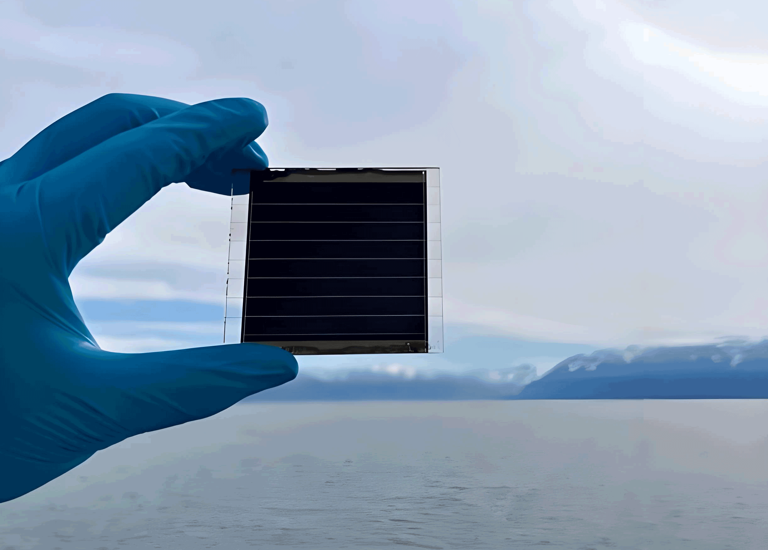
We fabricated perovskite solar cells using a blade-coating technique under ambient conditions. The perovskite precursor solution consisted of PbI2, FAI, MACl, and MAI in a mixed solvent of DMF and NMP, with a small amount of PEAI added to enhance crystallization. The HTL was formed by spin-coating a solution of MeO-2PACz in ethanol, either pure or mixed with MeO-PEAI (4 mg/mL). After annealing, an alumina layer was deposited to improve interface properties. The perovskite film was then blade-coated, followed by thermal annealing to form a highly crystalline layer. Finally, the ETL (C60 and SnO2) and silver electrode were deposited via thermal evaporation and atomic layer deposition, respectively. For modules, we used a 7 cm × 7 cm substrate with laser patterning to create series-connected subcells.
To evaluate the impact of MeO-PEAI passivation, we first examined the buried interface using scanning electron microscopy (SEM). Without passivation, the interface showed numerous PbI2 particles due to excess lead iodide in the precursor. In contrast, the passivated sample exhibited a significant reduction in PbI2 particles, suggesting that MeO-PEAI reacted with PbI2 to form a 2D perovskite. X-ray diffraction (XRD) confirmed this, with a distinct peak at 11° corresponding to the 2D perovskite phase. Additionally, X-ray photoelectron spectroscopy (XPS) revealed an increase in iodine content at the passivated interface, indicating successful incorporation of MeO-PEAI. Ultraviolet photoelectron spectroscopy (UPS) was used to determine the energy levels, showing that the passivated HTL had a higher HOMO level (−4.72 eV) compared to the pure SAM (−4.9 eV), which improved energy alignment with the perovskite layer.
We then fabricated perovskite solar cells with and without MeO-PEAI passivation. The current density-voltage (J-V) characteristics were measured under AM 1.5G illumination. The passivated devices showed a remarkable improvement in open-circuit voltage (Voc), from 1.02 V to 1.07 V, while maintaining high short-circuit current density (Jsc) and fill factor (FF). This resulted in an increase in PCE from 19.73% to 21.42% for the champion device. The statistical distribution of Voc and PCE across multiple devices demonstrated enhanced reproducibility with passivation, as shown in the table below:
| Condition | PCE (%) | Voc (V) | Jsc (mA/cm²) | FF |
|---|---|---|---|---|
| MeO-2PACz | 19.73 | 1.02 | 24.27 | 0.80 |
| MeO-2PACz + MeO-PEAI | 21.42 | 1.07 | 24.46 | 0.82 |
The external quantum efficiency (EQE) spectra and integrated current densities further validated these results, with the passivated device achieving a Jsc of 24.19 mA/cm², consistent with the J-V measurements. Steady-state photoluminescence (PL) and time-resolved photoluminescence (TRPL) measurements were performed on ITO/HTL/perovskite samples to assess charge carrier dynamics. The passivated sample exhibited faster PL quenching and shorter decay times, indicating improved hole extraction. The average TRPL decay time decreased from 891.95 ns to 468.46 ns with passivation, confirming reduced non-radiative recombination.
To quantify the defect density, we fabricated hole-only devices and measured their dark I-V characteristics. The trap-filled limit voltage (VTFL) was lower for the passivated device (0.65 V) compared to the control (0.70 V). Using the formula for defect density:
$$N_{\text{trap}} = \frac{2 \epsilon \epsilon_0 V_{\text{TFL}}}{e d^2}$$
where $\epsilon$ is the perovskite dielectric constant (35), $\epsilon_0$ is the vacuum permittivity, $e$ is the elementary charge, and $d$ is the film thickness (600 nm), we calculated defect densities of $7.5 \times 10^{15}$ cm⁻³ and $6.98 \times 10^{15}$ cm⁻³ for the control and passivated devices, respectively. This reduction in defect density aligns with the improved Voc and efficiency.
We also analyzed the diode ideality factor (n) from the light intensity dependence of Voc. The relationship is given by:
$$V_{\text{oc}} = V_{\text{oc,STC}} + \frac{n k_B T}{q} \ln \left( \frac{E_{\text{irra}}}{E_{\text{irra,STC}}} \right)$$
where $k_B$ is Boltzmann’s constant, $T$ is temperature, and $E_{\text{irra}}$ is the light intensity. The passivated device had an ideality factor of 1.47, closer to 1 than the control (1.64), indicating suppressed Shockley-Read-Hall recombination. Capacitance-voltage (C-V) measurements revealed a higher built-in potential (Vbi) for the passivated device (0.9 V) compared to the control (0.8 V), as determined from the Mott-Schottky plot:
$$\frac{1}{C^2} = -\frac{2(V – V_{\text{bi}})}{\epsilon \epsilon_0 q A^2 N}$$
where $A$ is the area and $N$ is the carrier density. The increased Vbi enhances the driving force for charge separation, contributing to higher performance.
To demonstrate scalability, we fabricated perovskite solar modules with an aperture area of 21.5 cm². The modules consisted of seven series-connected subcells defined by laser patterning (P1, P2, and P3 scribes). The passivated module achieved a PCE of 21.02%, with a Voc of 7.43 V, Isc of 76.23 mA, and FF of 0.80, outperforming the control module (PCE of 19.19%). The steady-state power output (SPO) over 300 seconds showed greater stability for the passivated module, with a PCE of 19.77% compared to 17.41% for the control. Additionally, maximum power point tracking (MPPT) under continuous illumination for 50 hours revealed that the passivated module retained 95% of its initial efficiency, while the control degraded to 93%. Under damp heat conditions (85°C and 85% relative humidity), the passivated module maintained 99% of its initial PCE after 1,000 hours, whereas the control dropped to 94%. These results underscore the robustness of the passivation strategy for large-scale applications.
The formation of a 2D perovskite at the buried interface via MeO-PEAI incorporation effectively passivates defects, reduces non-radiative recombination, and optimizes energy level alignment. This one-step modification simplifies fabrication and enhances both efficiency and stability. The champion perovskite solar cell achieved a PCE of 21.42%, and the module reached 21.02%, demonstrating the method’s scalability. Further improvements could involve optimizing the passivant concentration or exploring other organic cations. This work paves the way for high-performance, stable perovskite solar cells and modules suitable for commercial deployment.
In conclusion, our in-situ modification of the buried interface using MeO-PEAI in a SAM-based HTL significantly advances perovskite solar cell technology. By reducing interface defects and improving charge extraction, this approach enables high-efficiency devices with excellent reproducibility and stability. The successful fabrication of large-area modules confirms the practicality of this strategy for industrial applications. Future research will focus on extending this method to other perovskite compositions and tandem structures to further push the boundaries of photovoltaic performance.