
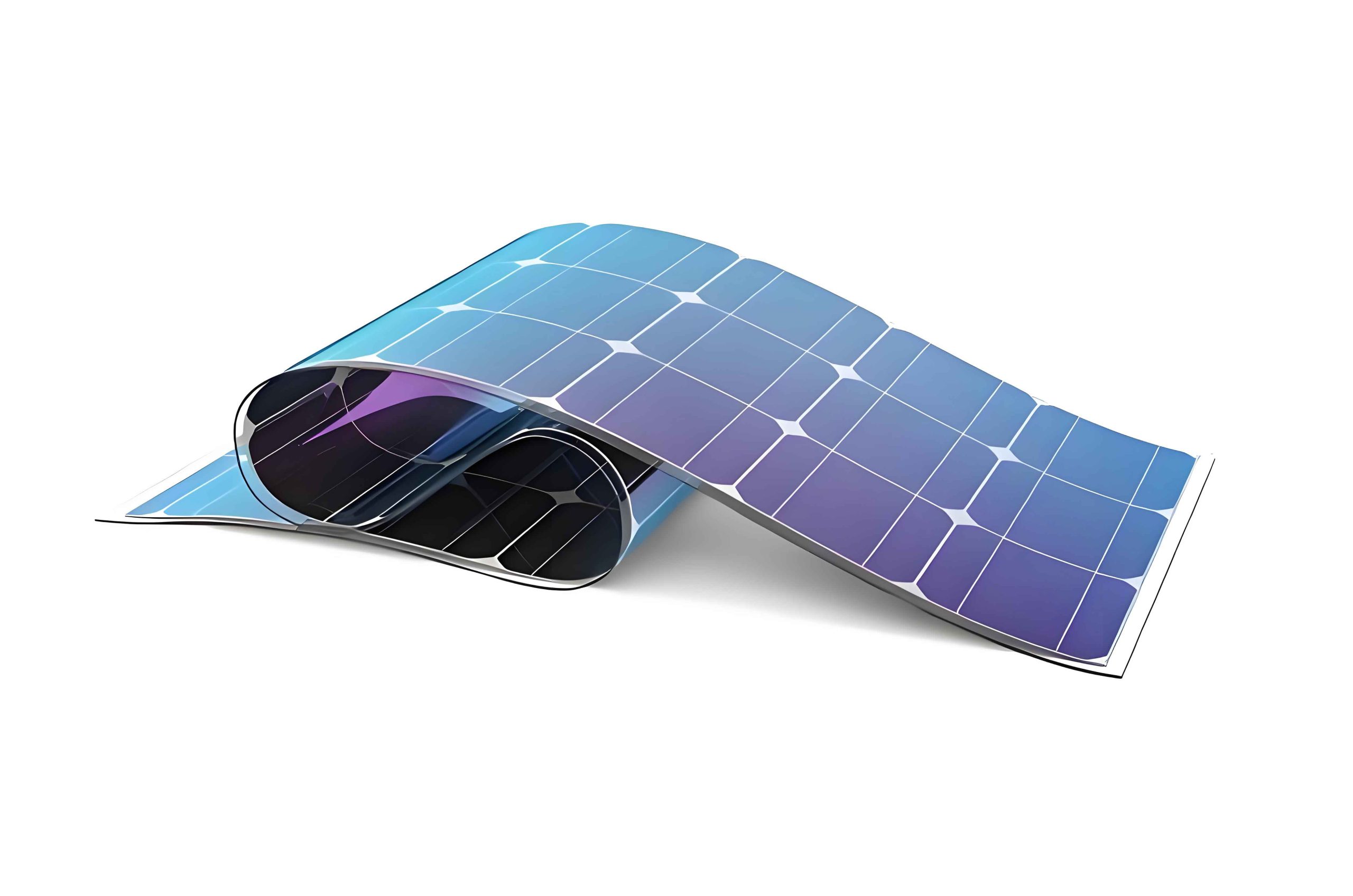
The escalating severity of environmental challenges, particularly air pollution, underscores an urgent need to transition from fossil fuels to sustainable and clean energy sources. Among the plethora of renewable options, solar energy stands out due to its sheer abundance; the amount of solar energy striking the Earth’s surface in one hour exceeds the planet’s total annual energy consumption. However, the current utilization of this immense resource remains disappointingly low, accounting for only about 1% of global energy demand, primarily through photovoltaic and photothermal conversion. This vast chasm between potential and reality is fundamentally rooted in the limitations of existing solar technology. My focus here is on a particularly promising technological avenue: the development and optimization of perovskite-based thin film solar panels.
At its core, a solar cell is a semiconductor device that converts photons directly into electricity via the photovoltaic effect. When light is absorbed, it generates electron-hole pairs (excitons). In a typical p-n junction cell, an internal electric field separates these charges, driving holes to the p-region and electrons to the n-region, thereby creating a potential difference. Connecting an external load completes the circuit, allowing electrical current to flow. The evolution of photovoltaic technology is often categorized into three generations. The first generation, dominated by crystalline silicon (c-Si) wafers—including monocrystalline and polycrystalline silicon—holds the largest market share. Despite their maturity and high efficiency, their production involves energy-intensive silicon purification processes, leading to higher costs and environmental impact. Second-generation solar cells, known as thin film solar panels, utilize materials like cadmium telluride (CdTe), copper indium gallium selenide (CIGS), and amorphous silicon (a-Si). They offer advantages in terms of material usage, weight, and potential for flexible applications, but concerns over material scarcity (e.g., indium) and toxicity (e.g., cadmium) have constrained their widespread adoption. The third generation encompasses emerging technologies that aim for high efficiency and low cost through novel materials and concepts. This includes dye-sensitized solar cells (DSSCs), quantum dot solar cells, organic photovoltaics (OPVs), and the rapidly advancing perovskite solar cells (PSCs). Perovskite thin film solar panels, in particular, have garnered unprecedented attention due to their exceptional optoelectronic properties, tunable bandgap, high absorption coefficients, long charge carrier diffusion lengths, and remarkably simple, low-cost solution-processable fabrication techniques.
The performance of any photovoltaic device, including perovskite thin film solar panels, is quantified by four key parameters: the power conversion efficiency (PCE or η), the short-circuit current density (JSC), the open-circuit voltage (VOC), and the fill factor (FF). The PCE is the ultimate figure of merit, defined as the ratio of the maximum electrical power output to the incident solar power input. It can be expressed as:
$$ \eta = \frac{P_{max}}{P_{in}} = \frac{J_{SC} \times V_{OC} \times FF}{P_{in}} $$
where Pin is the incident light power density (typically 100 mW/cm² under standard AM 1.5G illumination). JSC is the current density when the voltage across the device is zero, and it is primarily determined by the cell’s ability to absorb photons and collect the generated charge carriers. VOC is the voltage at which the net current is zero, representing the maximum potential the device can generate; it is fundamentally limited by the bandgap and is heavily influenced by non-radiative recombination losses. The FF is a measure of the “squareness” of the current density-voltage (J-V) curve, reflecting the quality of the diode and series/shunt resistances within the device. The typical ranges and interrelations for high-performance perovskite thin film solar panels are summarized below.
| Parameter | Symbol | Typical Range (Champion Cells) | Primary Determining Factors |
|---|---|---|---|
| Power Conversion Efficiency | PCE (η) | > 25% | Composite of JSC, VOC, FF |
| Short-Circuit Current Density | JSC | 24 – 26 mA/cm² | Absorption, charge generation & collection |
| Open-Circuit Voltage | VOC | 1.15 – 1.20 V | Bandgap, interfacial recombination |
| Fill Factor | FF | > 80% | Series/shunt resistance, charge transport |
The term “perovskite” in this context refers to a class of materials crystallizing in the structure of calcium titanate (CaTiO3), with a general chemical formula ABX3. In photovoltaic applications, the ‘A’ site is typically occupied by an organic cation like methylammonium (MA+, CH3NH3+), formamidinium (FA+, HC(NH2)2+), or inorganic cesium (Cs+); the ‘B’ site is a divalent metal ion, most commonly lead (Pb2+) or tin (Sn2+); and the ‘X’ site is a halide anion (I–, Br–, Cl–). The archetypal composition is MAPbI3. The ideal perovskite crystal structure is cubic, a configuration that offers optimal optoelectronic properties. In this phase, the B-site cation coordinates with six X-site anions to form [BX6]4- octahedra, which share corners to create a three-dimensional network. The larger A-site cation sits in the cuboctahedral cavities formed by eight neighboring octahedra, stabilizing the structure. The bandgap and electronic properties are critically influenced by the B-X bond length and the tilting of the [BX6] octahedra, which is tunable via compositional engineering (e.g., mixing A-site cations or halides).
The fabrication of high-quality, uniform, and pinhole-free perovskite thin films is paramount to achieving high-performance thin film solar panels. Several deposition techniques have been developed, each with its own merits and drawbacks, as outlined in the following comparison.
| Method | Process Description | Advantages | Disadvantages |
|---|---|---|---|
| One-Step Solution Coating | Precursor salts (e.g., PbI₂ and MAI) dissolved in a solvent are spin-coated onto a substrate, followed by thermal annealing. | Simple, fast, good stoichiometric control. | Difficult to control crystallization, often leads to incomplete coverage and small grains. |
| Two-Step Sequential Deposition | PbI₂ film is first deposited, then immersed in or coated with a solution of organic halide (e.g., MAI). | Better film morphology control, higher reproducibility, good for planar structures. | May lead to incomplete conversion, leaving unreacted PbI₂. |
| Vapor-Assisted Solution Process (VASP) | A PbI₂ film is prepared via solution processing, then exposed to MAI or FAI vapor in a controlled environment. | Produces large, highly crystalline grains, excellent film coverage. | Requires vacuum equipment, slower process, stoichiometry control can be challenging. |
| Dual-Source Thermal Evaporation | PbI₂ and organic halide (e.g., MAI) are evaporated simultaneously from separate sources in a high vacuum chamber. | Extremely uniform, pinhole-free films, excellent for multi-layer devices and large areas. | High equipment cost, low material utilization, potential for source corrosion. |
Despite the meteoric rise in efficiency, significant challenges remain for the commercialization of perovskite thin film solar panels. Key among these are long-term operational stability under heat, light, and moisture, and the mitigation of performance losses due to defects. High-efficiency devices often employ complex mixed-cation, mixed-halide compositions (e.g., (FAPbI3)0.97(MAPbBr3)0.03 with Cs+/Rb+ additives) to optimize bandgap and phase stability. However, these multi-component systems are prone to phase segregation and the formation of defect states at grain boundaries and interfaces. These defects act as traps for charge carriers, promoting non-radiative recombination, which directly reduces VOC and FF, and ultimately limits the PCE and stability. The defect density (Nt) relates to the recombination current (Jrec) and VOC loss (ΔV) as described by Shockley-Read-Hall (SRH) statistics:
$$ J_{rec} \approx q \cdot W \cdot N_t \cdot v_{th} \cdot \sigma \cdot n $$
$$ \Delta V = \frac{n k_B T}{q} \ln\left(1 + \frac{J_{rec}}{J_{ph}}\right) $$
where q is the elementary charge, W is the depletion width, vth is the thermal velocity, σ is the capture cross-section, n is the carrier density, kB is Boltzmann’s constant, T is temperature, and Jph is the photocurrent density.
This is where advanced passivation strategies become critical. Passivation involves the chemical or physical treatment of a surface or bulk to reduce its electronic activity—essentially, “healing” or deactivating defect sites. In-situ contact passivation is a powerful approach where the passivating agent is introduced during the fabrication process itself, often at the interface between the perovskite absorber layer and the charge transport layers (electron transport layer, ETL, or hole transport layer, HTL). This method is highly effective because it directly targets the most vulnerable and recombination-active regions of the device.
One innovative in-situ contact passivation method involves the use of volatile organic ammonium salts, such as formamidinium (FA) gas. Consider a state-of-the-art mixed perovskite film, for instance, one based on FA/MA/Cs. While Cs+ helps stabilize the black perovskite phase of FAPbI3 at room temperature, undesirable secondary phases like δ-CsPbI3 (a yellow, non-perovskite phase) can form. The process involves exposing the pre-formed, potentially defective perovskite thin film to a controlled atmosphere of FA gas (from a source like FAI powder under gentle heating). The FA molecules diffuse into the film, reacting with under-coordinated lead atoms (Pb0 or Pb2+ clusters) that often constitute deep-level traps. This reaction forms a thin, coherent shell of wide-bandgap FAPbI3 or a related complex at the grain boundaries and surfaces. This shell acts as a physical and electronic barrier, passivating the trap states. The mechanism can be conceptualized as:
$$ \text{Pb}^{0}/\text{Under-coordinated Pb}^{2+} + \text{FAI}_{(g)} \rightarrow \text{FAPbI}_{3(s)} \text{ (passivating layer)} $$
Furthermore, the FA treatment can promote the re-dissolution of undesirable secondary phases and facilitate cation exchange, leading to a more homogeneous and thermodynamically stable perovskite lattice.
The benefits of such an in-situ gas-phase passivation for thin film solar panels are multifaceted. First, it directly heals defects, suppressing non-radiative recombination. This is evidenced by a significant increase in photoluminescence (PL) intensity and carrier lifetime (τ), which directly translates to a higher VOC. Second, the formed FAPbI3 layer, with its suitable energy levels, can facilitate charge carrier extraction at the interface while blocking the opposite carrier, reducing interfacial recombination. Third, it enhances the film’s morphological stability against ion migration and phase segregation under operational stresses (light, heat, bias). The table below contrasts the characteristics of devices with and without this specific in-situ contact passivation.
| Device Characteristic | Without Passivation | With In-Situ FA Gas Passivation |
|---|---|---|
| Average VOC (V) | ~1.10 | ~1.17 – 1.19 |
| Photoluminescence Lifetime (τ, ns) | 100 – 300 | 500 – 1000+ |
| Trap Density (Nt, cm⁻³) | High (10¹⁶ – 10¹⁷) | Low (10¹⁵ – 10¹⁶) |
| Champion PCE | ~19% | > 21% |
| FF | < 78% | > 81% |
| Stability (T80 under 1 Sun) | Several hundred hours | Significantly extended (>1000 hours) |
| Device-to-Device Reproducibility | Moderate (high variance in VOC) | High (tight parameter distribution) |
The concept of in-situ contact passivation extends beyond FA gas. A wide variety of molecular, ionic, and polymeric agents have been explored. These can be introduced via additives in the precursor solutions, post-treatment solutions, or interlayers deposited before the charge transport layer. Common passivating agents include Lewis bases (e.g., thiophene, pyridine derivatives) that donate electron density to under-coordinated Pb2+, alkylammonium halides (e.g., phenethylammonium iodide, PEA+) that form 2D perovskite capping layers, and polymers or small molecules that physically encapsulate grains. The effectiveness of a passivant (ξ) can be semi-quantitatively related to its ability to bind to defects and its impact on interfacial energy alignment. A simple metric is the passivation-induced change in quasi-Fermi level splitting (ΔEF), which correlates with VOC:
$$ \Delta V_{OC} \approx \frac{\Delta E_F}{q} = \frac{k_B T}{q} \ln\left(\frac{PL_{passivated}}{PL_{unpassivated}}\right) $$
where PL denotes the integrated photoluminescence intensity.
In conclusion, the pursuit of high-efficiency, stable, and commercially viable perovskite thin film solar panels hinges on mastering defect control. In-situ contact passivation methods represent a sophisticated and highly effective toolkit for addressing this fundamental challenge. By integrating passivating agents directly during the fabrication process—whether through gas-phase treatments, solution additives, or engineered interlayers—we can simultaneously heal bulk and interfacial defects, suppress non-radiative recombination, improve charge extraction, and enhance environmental stability. The FA gas treatment exemplifies how a simple process can yield a synergistic enhancement in VOC, FF, and operational lifetime. As research progresses, the development of novel, multi-functional passivants and their integration into scalable manufacturing processes will be crucial. The ultimate goal is to translate the phenomenal laboratory performance of perovskite thin film solar panels into durable, high-performance modules that can reliably contribute to the global clean energy landscape, helping to bridge the gap between the immense potential of solar energy and our current utilization of it.