
In recent years, inorganic cesium lead halide perovskites, particularly CsPbI2Br, have emerged as promising light-absorbing materials for next-generation photovoltaic devices due to their exceptional thermal stability, suitable bandgap, and high charge carrier mobility. However, the performance of CsPbI2Br perovskite solar cells is often limited by interfacial defects and inefficient charge extraction at the buried interface between the electron transport layer and the perovskite layer. In this study, I present a facile in situ strategy to modify the buried interface by incorporating 4-mercaptophenylboronic acid (4-MPBA) into the CsPbI2Br precursor solution. During perovskite crystallization, 4-MPBA molecules are excluded from the lattice and accumulate at the TiO2/CsPbI2Br interface, forming a dipolar interlayer that enhances interfacial contact, reduces defects, and optimizes energy level alignment. As a result, the carbon-based, hole-transport-layer-free CsPbI2Br perovskite solar cell achieves a power conversion efficiency (PCE) of 14.83%, a 26% improvement over the control device. Additionally, the modified devices exhibit superior stability, retaining over 90% of their initial PCE after 40 days of storage in ambient air. This work underscores the importance of in situ buried interface engineering for advancing inorganic perovskite solar cells.
The fabrication of CsPbI2Br perovskite films involved a one-step solution processing method. A precursor solution was prepared by dissolving PbI2 and CsBr in dimethyl sulfoxide (DMSO) at a concentration of 1 mol/L. For the modified samples, 0.8 mg of 4-MPBA was added to the precursor solution. The solution was then spin-coated onto a TiO2-coated FTO substrate at 3000 rpm, followed by thermal annealing at 220°C for 8 minutes to form the crystalline perovskite layer. A carbon electrode was deposited via blade-coating to complete the device structure. Characterization techniques included scanning electron microscopy (SEM), X-ray diffraction (XRD), ultraviolet-visible (UV-Vis) spectroscopy, X-ray photoelectron spectroscopy (XPS), ultraviolet photoelectron spectroscopy (UPS), photoluminescence (PL) spectroscopy, and electrochemical measurements. Density functional theory (DFT) calculations were performed to analyze the adsorption behavior of 4-MPBA on TiO2.
The incorporation of 4-MPBA significantly influenced the morphology and interfacial properties of the CsPbI2Br perovskite layer. Cross-sectional SEM images revealed that the control sample exhibited poor interfacial contact with the TiO2 layer, characterized by voids and pinholes. In contrast, the 4-MPBA-modified sample showed a compact and uniform interface, indicating enhanced adhesion and reduced defects. This improvement is attributed to the in situ formation of a 4-MPBA interlayer, which acts as a bridge between the TiO2 and perovskite layers. XPS analysis of the O 1s peak for TiO2 with and without the 4-MPBA interlayer demonstrated a shift to lower binding energy and a reduction in the peak area associated with oxygen vacancies (OII), confirming defect passivation. The decreased trap density was further quantified using the trap-filled limit voltage (VTFL) from space-charge-limited current (SCLC) measurements in electron-only devices. The VTFL decreased from 1.04 V for the control to 0.82 V for the 4-MPBA-modified device, indicating a lower defect density in the perovskite layer.
To elucidate the interaction between 4-MPBA and TiO2, DFT calculations were performed. The adsorption energy (Ead) was calculated for different configurations, and the most stable adsorption mode involved bidentate coordination of the -B(OH)2 group to TiO2, with an Ead of -2.45 eV. This strong interaction facilitates the formation of a oriented dipole layer at the interface, which modulates the energy level alignment. UPS measurements showed that the work function of TiO2 shifted from -4.39 eV to -4.16 eV upon 4-MPBA modification, while the valence band maximum (VBM) changed from -7.47 eV to -7.35 eV. The Tauc plot derived from UV-Vis spectra confirmed that the bandgap of TiO2 remained unchanged at approximately 3.2 eV. Thus, the conduction band minimum (CBM) of TiO2 shifted from -4.09 eV to -3.97 eV, resulting in a more favorable energy level alignment with the CBM of CsPbI2Br (around -3.8 eV). This reduction in the energy offset enhances electron extraction and reduces interfacial recombination.
The defect passivation effect of 4-MPBA was further investigated through steady-state PL spectroscopy. CsPbI2Br films deposited on glass substrates exhibited a significant increase in PL intensity when modified with 4-MPBA, indicating suppressed non-radiative recombination. When deposited on TiO2/FTO substrates, the PL quenching was more pronounced for the 4-MPBA-modified sample, demonstrating efficient electron transfer from the perovskite to TiO2. The enhanced charge extraction is critical for improving the performance of perovskite solar cells. The charge carrier dynamics were analyzed using electrochemical impedance spectroscopy (EIS), which revealed a lower charge transfer resistance and higher recombination resistance for the modified devices.
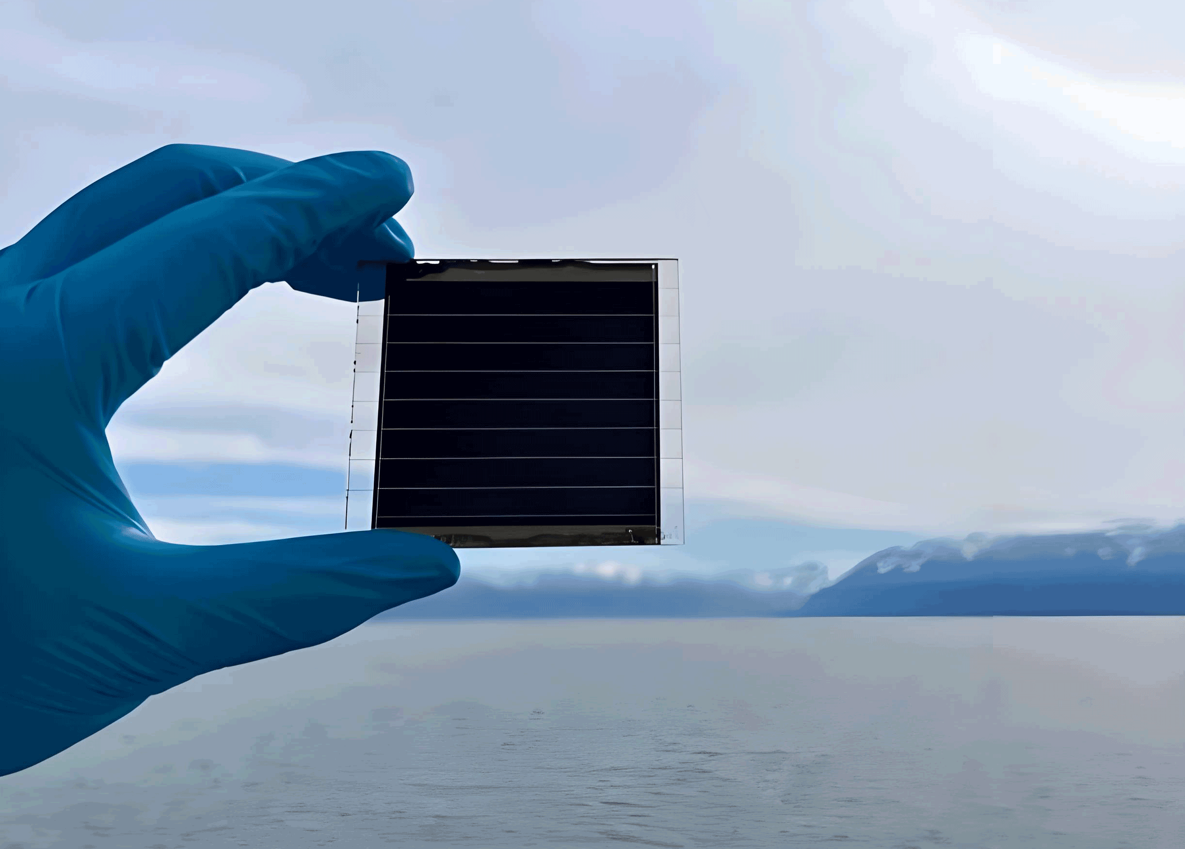
The photovoltaic performance of the carbon-based CsPbI2Br perovskite solar cells was evaluated under AM1.5G illumination. The current density-voltage (J-V) curves for the control and 4-MPBA-modified devices are shown in Figure 5a, and the key parameters are summarized in Table 1. The control device achieved a PCE of 11.71%, with an open-circuit voltage (Voc) of 1.25 V, a short-circuit current density (Jsc) of 14.64 mA/cm2, and a fill factor (FF) of 0.64. In contrast, the 4-MPBA-modified device exhibited a PCE of 14.83%, with Voc = 1.31 V, Jsc = 15.72 mA/cm2, and FF = 0.72. The improvement in Voc is attributed to reduced non-radiative recombination, while the enhanced Jsc and FF result from improved charge extraction and collection. The external quantum efficiency (EQE) spectra confirmed the higher photocurrent generation in the modified device across the visible spectrum.
| Sample | Voc (V) | Jsc (mA/cm2) | FF | PCE (%) |
|---|---|---|---|---|
| Without 4-MPBA | 1.25 | 14.64 | 0.64 | 11.71 |
| With 4-MPBA | 1.31 | 15.72 | 0.72 | 14.83 |
The stability of the perovskite solar cells was assessed under ambient conditions (25±5°C, 35±10% relative humidity) without encapsulation. The control device retained only 30% of its initial PCE after 20 days, whereas the 4-MPBA-modified device maintained over 90% of its initial PCE after 40 days. This enhanced stability is due to the passivation of interfacial defects and the suppression of ion migration by the 4-MPBA interlayer. Additionally, under continuous illumination at 100 mW/cm2 for 100 hours, the modified device retained 97.3% of its initial PCE, demonstrating excellent photostability.
To further quantify the interface properties, I derived the defect density (Nt) using the SCLC method with the formula:
$$N_t = \frac{2 \epsilon_0 \epsilon_r V_{TFL}}{e L^2}$$
where ε0 is the vacuum permittivity, εr is the relative permittivity of CsPbI2Br (approximately 25), e is the elementary charge, and L is the thickness of the perovskite layer (about 500 nm). For the control device, Nt was calculated as 1.2 × 1016 cm-3, while for the 4-MPBA-modified device, it reduced to 8.5 × 1015 cm-3. This reduction in defect density directly correlates with the improved photovoltaic parameters.
The energy level alignment at the TiO2/CsPbI2Br interface can be described by the band offset ΔEC:
$$\Delta E_C = E_{C,TiO2} – E_{C,CsPbI2Br}$$
where EC,TiO2 and EC,CsPbI2Br are the conduction band energies of TiO2 and CsPbI2Br, respectively. For the control device, ΔEC was approximately 0.29 eV, which was reduced to 0.17 eV after 4-MPBA modification. This smaller offset facilitates electron injection and reduces energy loss, contributing to the higher Voc and Jsc.
In conclusion, the in situ formation of a 4-MPBA interlayer at the buried interface of CsPbI2Br perovskite solar cells effectively enhances interfacial properties, leading to significant improvements in efficiency and stability. This strategy provides a versatile approach for optimizing inorganic perovskite solar cells and paves the way for their commercial application. Future work will focus on extending this method to other perovskite compositions and scaling up device fabrication.
The development of high-performance perovskite solar cells relies on meticulous interface engineering. The results presented here demonstrate that in situ modification of the buried interface is a powerful tool for achieving efficient and stable inorganic perovskite solar cells. By understanding the molecular interactions and charge transport mechanisms, we can further optimize these devices for real-world applications.