
As energy and environmental challenges intensify, solar energy has emerged as a critical renewable resource. The proliferation of solar power facilities necessitates advanced inverters, where Power Integration Modules (PIMs) from onsemi deliver high efficiency and reliability. This article explores solar inverter architectures, topologies, design considerations, and practical implementations.
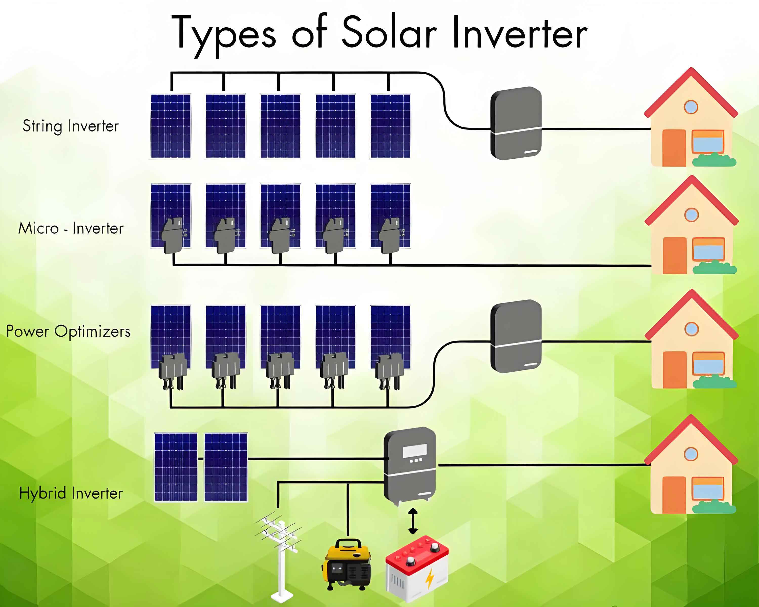
Solar Inverter, UPS, and ESS Architectures
Modern solar inverters, Uninterruptible Power Supplies (UPS), and Energy Storage Systems (ESS) share structural similarities. A typical 20–200 kVA solar inverter includes:
- Boost inductors
- DC-DC boost modules
- DC-link capacitors
- 3-level inverter modules
- AC filtering components
The efficiency advantage of multi-level inverters over conventional 2-level designs is quantified by:
$$ \eta_{\text{3-level}} = \frac{P_{\text{out}}}{P_{\text{in}}} \approx 98\% $$
compared to 95–96% for 2-level systems. Reduced THD (<5%) and smaller filters further enhance grid compatibility.
Three-Level Inverter Topologies
Three dominant 3-level configurations for solar inverters are compared below:
| Topology | Switching Loss | Parasitic Inductance | Application Range |
|---|---|---|---|
| T-Type (TNPC) | Low | Moderate | 20–150 kW |
| Neutral Point Clamped (NPC) | Medium | High | Legacy Systems |
| Active NPC (ANPC) | Medium | Low | High-Frequency Designs |
PIM Selection Guide for Solar Inverters
Key parameters for selecting power modules in solar inverter designs:
| Module Type | Voltage Rating | Current Capacity | Package | Application |
|---|---|---|---|---|
| NXH80B120H2Q0 | 1200V | 80A | Q0 | 25kW Boost |
| NXH160T120L2Q2 | 1200V | 160A | Q2 | 90kW Inverter |
| NXH400T150L3Q2 | 1500V | 400A | Q2+ | 220kW Utility |
The power derating curve for solar inverter modules follows:
$$ P_{\text{max}}(T) = P_{\text{nom}} \times \left(1 – \frac{T_j – 25^\circ C}{150}\right) $$
where \( T_j \) represents junction temperature.
Design Implementation Example
A 60kW solar inverter implementation using 3-level TNPC topology demonstrates:
- DC input: 600–1000V
- Boost stage efficiency: 99.2%
- Inverter stage efficiency: 98.7%
Total system losses are calculated as:
$$ P_{\text{loss}} = P_{\text{boost}} + P_{\text{inv}} = \frac{P_{\text{out}}}{0.992} – P_{\text{out}} + \frac{P_{\text{out}}}{0.987} – P_{\text{out}} $$
Gate Drive Considerations
Critical parameters for IGBT gate drivers in solar inverters:
- CMTI > 100 kV/μs
- Optimal gate resistance \( R_g \):
$$ R_g = \sqrt{\frac{L_{\text{stray}}}{C_{\text{ies}}}} $$
where \( L_{\text{stray}} \) represents parasitic inductance (typically 10–30 nH).
Thermal Management
Junction temperature estimation for solar inverter modules:
$$ T_j = T_a + R_{\theta j-a} \times P_{\text{loss}} $$
For Q2 package modules:
$$ R_{\theta j-a} \approx 0.25^\circ C/W $$
Future Trends
Emerging technologies in solar inverter development include:
- SiC/GaN hybrid modules
- Bidirectional H6.5 topology
- AI-based MPPT algorithms
These advancements promise to push solar inverter efficiencies above 99% while reducing LCOE (Levelized Cost of Energy) by 15–20%.