
In the context of global efforts toward carbon peak and carbon neutrality, the integration of clean energy sources like solar power into the grid has become a critical research focus. Solar inverters, as the key interface between photovoltaic (PV) systems and the grid, play a vital role in converting direct current (DC) from PV modules into alternating current (AC) for grid connection. The performance and reliability of solar inverters directly impact the efficiency and safety of PV power generation systems. With the trend toward miniaturization, lightweight design, and higher power density in solar inverters, effective thermal management has emerged as a significant challenge. Over 55% of failures in electronic devices are attributed to overheating, making散热设计 essential for ensuring stable operation. This study addresses the散热问题 of Insulated Gate Bipolar Transistor (IGBT) modules, which are core components in high-power solar inverters, by proposing a forced air cooling optimization scheme. We focus on reducing the thermal resistance between the IGBT chips and the environment through fan selection and heat sink design, ensuring that junction temperatures remain within safe limits while minimizing material costs.
The development of solar inverters has been driven by the need for higher efficiency and compactness. As solar inverter power ratings increase, the thermal loads on internal components, particularly IGBT modules, escalate. IGBT modules generate substantial heat due to switching and conduction losses, and excessive temperatures can lead to reduced reliability or failure. In this work, we analyze the thermal pathways and equivalent thermal resistances of IGBT modules to establish design criteria. We then proceed with fan selection based on air volume calculations and optimize the heat sink using a multi-objective approach that balances散热效果 and weight. The optimization involves design of experiments (DOE), cost function analysis, and response surface methodology to identify the best parameters. Our results demonstrate that the optimized design keeps both the heat sink temperature and IGBT junction temperature well below standard requirements, with margins exceeding 10°C. This approach provides a reference for the散热设计 of similar solar inverter products, contributing to the advancement of reliable and cost-effective PV systems.
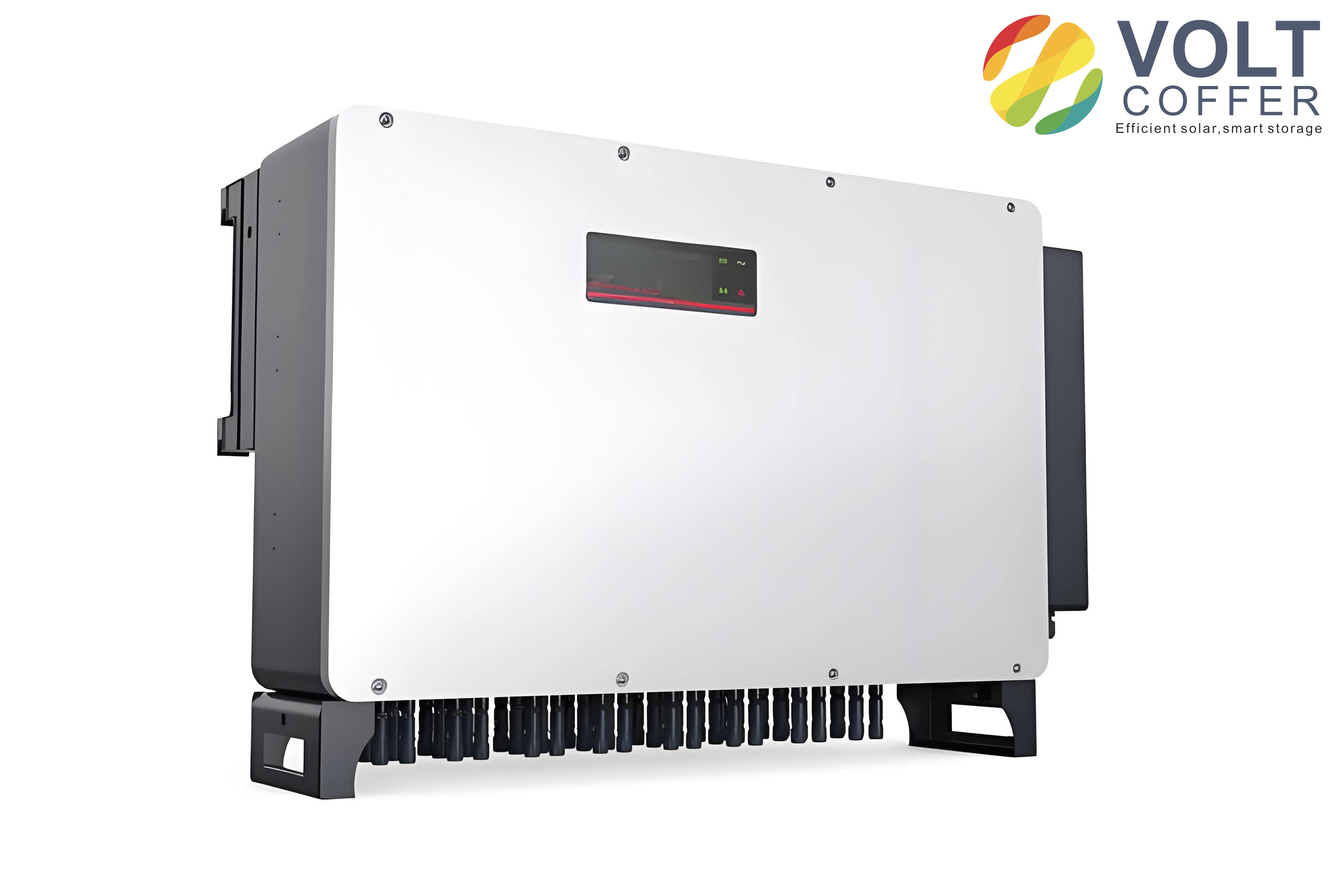
Simulation Model for Solar Inverter Thermal Analysis
To address the散热挑战 in a 60 kW high-power solar inverter, we simplified the model to focus on critical components, including the IGBT modules, heat sink, fans, enclosure, air ducts, and PCB. The IGBT modules, with the highest power density and heat generation, are the primary targets for散热设计. Other components, with lower power dissipation, rely on natural convection and are not detailed in this analysis. The simplified model, as illustrated in the following figure, retains essential features for accurate thermal simulation.
The materials used in the solar inverter model include AL6061 for the enclosure and heat sink, thermal grease for the interface, PBT for the module casing, copper for the substrate, and FR4 for the PCB. Table 1 summarizes the materials and their thermal conductivities, which are crucial for heat transfer calculations.
| Component | Material | Thermal Conductivity (W/(m·K)) |
|---|---|---|
| Inverter Enclosure | AL6061 | 180 |
| Heat Sink | AL6061 | 180 |
| Thermal Interface Material | Thermal Grease | 2 |
| Power Module Casing | PBT | 0.27 |
| Power Module Substrate | Copper | 385 |
| PCB Board | FR4 | 0.35 |
The power losses in the IGBT modules consist of conduction and switching losses for both the IGBTs and freewheeling diodes (FWDs). Using manufacturer-provided loss simulation software, we calculated the IGBT power dissipation as 106 W and the FWD dissipation as 194 W per module, resulting in a total of 300 W per module. The IGBT module was modeled in detail, incorporating multiple layers such as chips, solder, and substrate, to accurately capture heat flow. The simulation model accounts for these losses and material properties to predict temperature distributions under operating conditions. This detailed modeling is essential for reliable散热分析 in solar inverters, as it enables us to identify hotspots and optimize the cooling system effectively.
Thermal Resistance Analysis of IGBT Modules in Solar Inverters
The junction temperature (T_j) of IGBT chips must not exceed standard limits to ensure reliability in solar inverters. Since direct measurement of chip temperature is impractical due to complex packaging, we analyze the thermal resistance network to infer T_j from case or heat sink temperatures. The heat generated by the chips flows through multiple layers, including encapsulation and solder, to the heat sink base and fins, where it is dissipated to the ambient air via convection. The equivalent thermal resistance from junction to ambient (R_total) can be expressed as:
$$ R_{total} = R_{th,jc} + R_{th,ch} + R_{th,ha} $$
where R_th,jc is the junction-to-case thermal resistance, R_th,ch is the case-to-heat sink thermal resistance, and R_th,ha is the heat sink-to-ambient thermal resistance. R_th,jc is fixed by manufacturing and materials, while R_th,ch is negligible compared to R_th,ha. Thus, reducing R_total primarily involves minimizing R_th,ha through enhanced convection. For the IGBT modules in this solar inverter, the maximum allowable junction temperature T_j,max is 150°C, and we design for 80% of this value, i.e., T_j ≤ 120°C. The power dissipation per module P_V is 300 W. The maximum allowable heat sink temperature T at the IGBT module location is given by:
$$ T = 0.8 \times T_{j,max} – P_V \times (R_{th,jc} + R_{th,ch}) $$
Based on manufacturer data, R_th,jc and R_th,ch values are obtained, and calculations yield T ≤ 100°C. Therefore, the散热设计 criteria for this solar inverter are: IGBT chip junction temperature must not exceed 120°C, and the heat sink temperature at the IGBT module position must not exceed 100°C. Meeting these criteria ensures the long-term reliability of the solar inverter under high-power conditions.
Heat Dissipation Optimization Design for Solar Inverters
To achieve effective thermal management in the solar inverter, we focus on reducing the heat sink-to-ambient thermal resistance R_th,ha through fan selection and heat sink optimization. This section details the methods used for both aspects, incorporating calculations and simulations to derive an optimal solution.
Fan Selection for Forced Air Cooling
Fan selection is critical in forced air cooling systems for solar inverters. The required air volume Q can be estimated using the heat balance equation:
$$ Q = \frac{P}{\rho C_p \Delta T} $$
where P is the total power dissipated by components cooled by air (in watts), ρ is the air density (in kg/m³), C_p is the specific heat capacity of air (in kJ/(kg·°C)), and ΔT is the temperature difference between outlet and inlet air (in °C). For this solar inverter, the ambient temperature is 55°C, and ΔT is set to 15°C, resulting in an average air temperature T_f of 62.5°C. At this temperature, air properties are ρ = 1.1 kg/m³ and C_p = 1009 J/(kg·°C). The total power P for air-cooled components is 900 W (for three IGBT modules). Substituting these values:
$$ Q = \frac{900}{1.1 \times 1009 \times 15} \approx 0.054 \, \text{m}^3/\text{s} = 114.63 \, \text{CFM} $$
where 1 CFM ≈ 0.028 m³/min. Accounting for design margins of 1.5 to 2 times the ideal value, the total fan air volume should be at least 171.95 CFM. Using two fans in parallel, each fan must provide a minimum of 85.97 CFM. We selected fans with a maximum air volume of 132 CFM each, ensuring sufficient cooling capacity for the solar inverter. This fan selection supports adequate airflow through the heat sink, enhancing convective heat transfer in the solar inverter enclosure.
Heat Sink Optimization Using Cost Function and Response Surface Methodology
The initial heat sink design did not meet the散热 requirements for the solar inverter, necessitating optimization. Key parameters affecting heat sink performance include base plate thickness, fin thickness, number of fins, fin height, length, and width. Given space constraints in the solar inverter enclosure, we optimized fin thickness, base plate thickness, number of fins, and heat sink length. These parameters influence both散热效果 and heat sink mass, which relates to material cost and structural integrity. Thus, we employed a multi-objective optimization to find a balance between minimizing IGBT base plate temperature and heat sink mass.
First, we conducted a single-variable analysis to understand the impact of each parameter on IGBT base plate temperature and heat sink mass. The baseline heat sink parameters are: length L = 322.8 mm, base plate thickness d = 8 mm, fin thickness t = 1.5 mm, and number of fins n = 43. Figure 1 (not shown) illustrates the trends: as fin thickness, number of fins, base plate thickness, and length increase, IGBT base plate temperature decreases, but heat sink mass increases linearly. Based on these trends and manufacturing constraints, we defined the optimization intervals, as shown in Table 2.
| Parameter | Unit | Optimization Interval |
|---|---|---|
| Fin Thickness | mm | [1.5, 4.5] |
| Number of Fins | – | [43, 68] |
| Base Plate Thickness | mm | [8, 16] |
| Heat Sink Length | mm | [322.8, 352.8] |
For multi-objective optimization, we generated 40 DOE schemes in the Command Center module, with 10 variables per parameter. To avoid local optima, we used a cost function based on scoring analysis. The steps are as follows:
- For the 40 DOE schemes, find the maximum and minimum IGBT base plate temperatures (T_max and T_min) and heat sink masses (M_max and M_min).
- Calculate the score for each scheme’s temperature (R_T) and mass (R_M) using:
$$ R_T = \frac{T_{max} – T_i}{T_{max} – T_{min}} \times 100 $$
$$ R_M = \frac{M_{max} – M_i}{M_{max} – M_{min}} \times 100 $$
where T_i and M_i are the temperature and mass for scheme i, respectively. Scores range from 0 (worst) to 100 (best). - Define the cost function f as a weighted sum:
$$ f = \omega_1 R_T + \omega_2 R_M $$
where ω_1 and ω_2 are cost weights satisfying ω_1 + ω_2 = 1 and ω_1, ω_2 ∈ [0,1]. These weights reflect the relative importance of temperature and mass. - Evaluate multiple weight combinations (ω_1, ω_2) and select the scheme with the lowest f for each combination. After comparison, we determined the optimal weights as ω_1 = 0.4 and ω_2 = 0.6, emphasizing mass reduction while maintaining adequate散热效果 for the solar inverter.
Next, we performed response surface optimization on the 40 DOE schemes to identify the optimal parameter set. The response surfaces, as shown in Figure 2 (not shown), reveal interactions between parameters. For instance:
– As heat sink length increases, the cost function decreases, with a minimum near L = 352.8 mm.
– As base plate thickness increases, the cost function increases, with a minimum near d = 8 mm.
– Fin thickness in the range [1.5, 2.1] mm minimizes the cost function.
– The number of fins between 53 and 63 minimizes the cost function.
Integrating these findings, the response surface optimization yielded the optimal heat sink parameters listed in Table 3. The resulting heat sink has a mass of 14.07 kg, and the IGBT base plate temperatures are between 86.87°C and 88.88°C, well below the 100°C limit. This optimized design ensures that the solar inverter operates reliably without overheating.
| Parameter | Optimal Value |
|---|---|
| Heat Sink Length (mm) | 352.8 |
| Base Plate Thickness (mm) | 8 |
| Fin Thickness (mm) | 1.68 |
| Number of Fins | 68 |
| Heat Sink Mass (kg) | 14.07 |
| IGBT 1 Base Plate Temperature (°C) | 86.87 |
| IGBT 2 Base Plate Temperature (°C) | 88.21 |
| IGBT 3 Base Plate Temperature (°C) | 88.88 |
Results and Discussion
The optimized散热设计 for the solar inverter was validated through simulation. The maximum heat sink temperature at the IGBT module location is 87.8°C, which is 12.2°C below the 100°C requirement. The maximum IGBT chip junction temperature is 109°C, 11°C below the 120°C limit. These margins provide a safety buffer for variations in operating conditions, such as ambient temperature fluctuations or increased load. The use of forced air cooling with optimized fans and heat sink effectively manages the thermal loads in the solar inverter, demonstrating the success of our approach. The cost function-based optimization allowed us to achieve a balance between performance and cost, which is crucial for commercial solar inverter products. This method can be extended to other solar inverter designs, promoting the development of efficient and reliable PV systems.
Conclusion
In this study, we developed a comprehensive散热分析和优化设计 for high-power solar inverter IGBT modules. By analyzing thermal resistance pathways and employing forced air cooling, we established design criteria and selected appropriate fans based on air volume calculations. The heat sink was optimized using a cost function and response surface methodology, resulting in a lightweight design that maintains IGBT temperatures within safe limits. The final design ensures heat sink and junction temperatures are more than 10°C below standard requirements, providing ample margin for reliability. This work offers valuable insights and a reference for the thermal management of solar inverters, supporting the trend toward smaller, lighter, and more powerful PV systems. Future research could explore advanced cooling techniques, such as liquid cooling or phase-change materials, for next-generation solar inverters.