
The photovoltaic grid-connected controller is mainly composed of a power module, a staggered flyback module, a full bridge module, and a feedback module.The controller is mainly responsible for converting DC signals to AC signals. DC power flows from the photovoltaic panel into the corresponding voltage reducer, reducing it to the voltage value (12V, 5V, 3.3V) required for the operation of the drive system. The staggered flyback circuit converts the DC signal to a full-wave signal under the drive of the flyback drive circuit (consisting of corresponding field-effect transistors).The full-wave signal is then converted into a preliminary sine wave signal in the full bridge circuit due to the opening and closing of the bridge circuit.At this point, the sine wave signal needs to be filtered and regulated before being used in the power grid (to prevent interference with the power grid).Of course, during the signal conversion process between the staggered flyback circuit and the full bridge circuit, various feedback circuits are detected in real time.The feedback signals detected in the controller are processed by preamplification, bandpass filtering, and differential processing, and then finally processed, displayed, and output in the DSP chip.
1. Design of power module
The auxiliary power supply module provides power to all on-board components, including the TMS320F28035, gate drive IC, and operational amplifier.
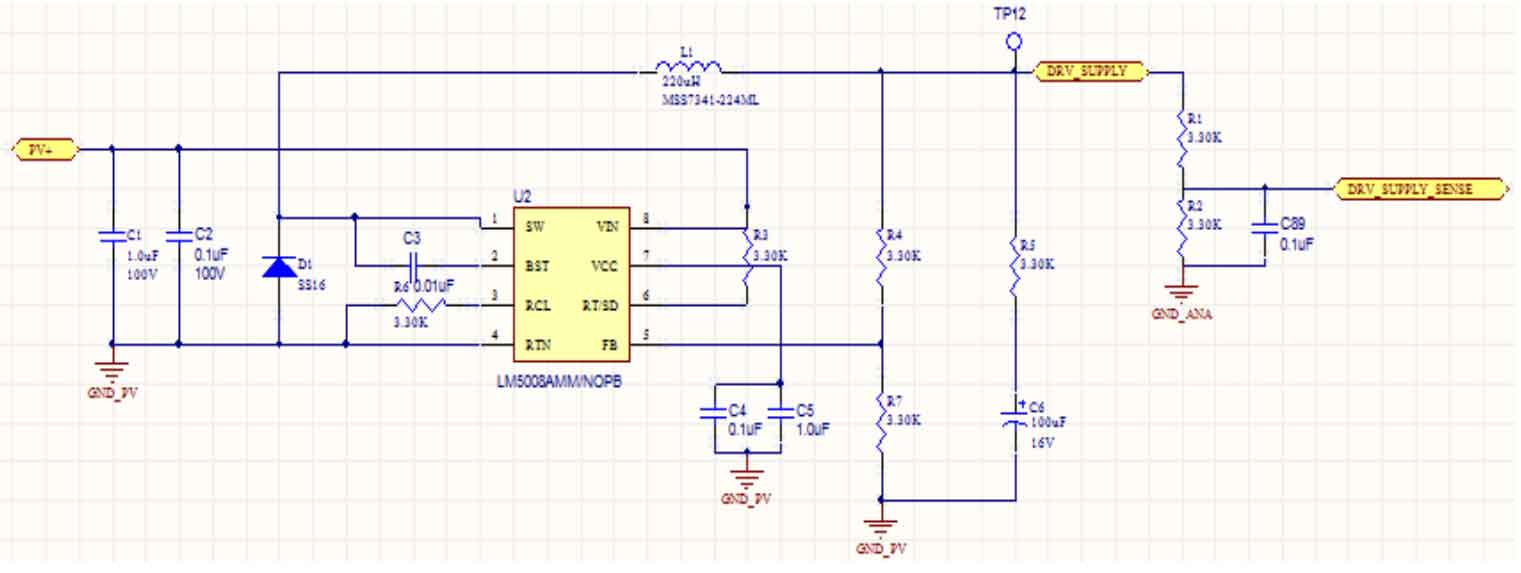
Due to functional requirements, the designed circuit must include three buck circuits (12V, 5V, and 3.3V) to power the corresponding modules.A buck switching regulator (LM5008A) with a constant on-time is connected to the PV module to generate a regulated output of 12V to drive the flyback MOSFET, full-bridge MOSFET, and other auxiliary power supply components.
Figure 1 shows the 12V drive power circuit.
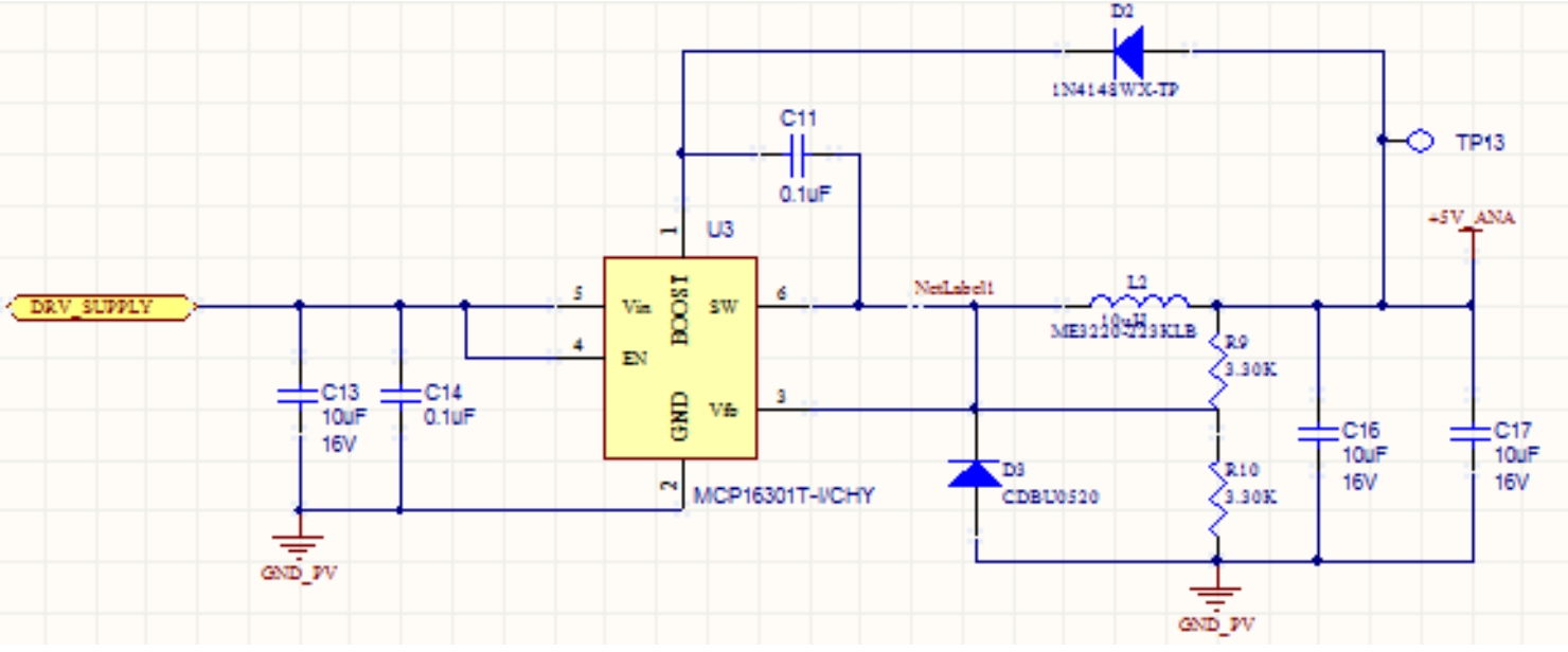
Another buck regulator (MCP16301) is responsible for reducing the 12V drive power to 5V and providing it to the optoelectronic isolation error amplifier, rail-to-rail operational amplifier, and linear current sensor IC.Figure 2 shows the buck circuit from 12V to 5V.
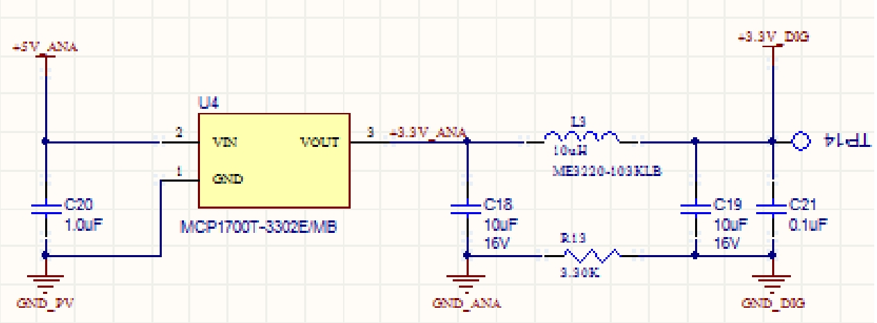
Use a low quiescent current LDO regulator to generate a 3.3V drive power supply for the F28035 and on-board temperature sensors.Figure 3 shows the buck circuit that reduces 5V to 3.3V.
2. Design of interleaved flyback module
Two topologies are available: flyback converters and forward converters.Among them, flyback converters are generally used for low-power buck applications with hundreds of watts of power and low output currents.Forward converters can also boost the voltage of PV panels and provide current isolation.However, because flyback converters require fewer components (no output freewheeling diodes or inductors), they are chosen.
The biggest problem with flyback topology is how to deal with the leakage energy.This solar inverter integrates an active clamp circuit, which has a clamp capacitor dedicated to storing the leakage energy.This energy is then transferred to the secondary, enabling energy recovery.The active clamp circuit can also provide zero-voltage switching for the flyback MOSFET, which will reduce switching losses and improve overall efficiency.The schematic diagram of a single-phase active clamp flyback converter is shown in Figure 4.
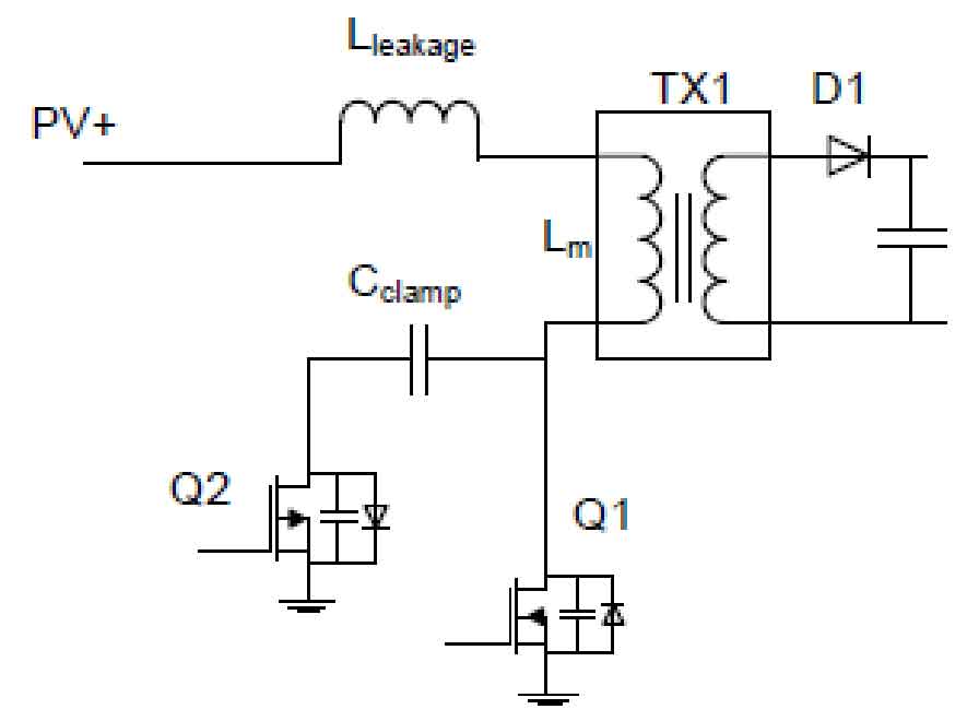
Figure 5 shows the drive circuit for a single-phase drive MOSFET.
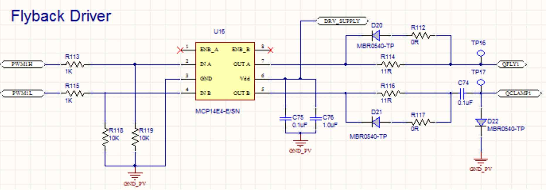
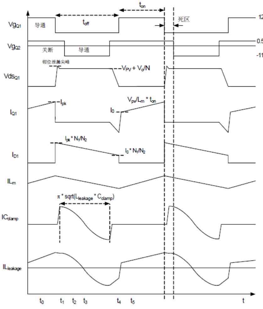
To drive the P-channel MOSFET, a negative voltage is required between the gate and source.The output of the gate drive IC (MCP14E4) is a square wave with a given amplitude (12V) and duty cycle (50%).The role of the ceramic capacitor is to eliminate DC bias, and the diode (anode connected to the capacitor, cathode grounded) is connected after the capacitor to clamp the positive voltage at around 0.7V and make the amplitude all negative.Figure 6 shows the gate drive waveform of two field-effect transistors (MOSFETs).
2.1 Selection of working mode
When designing a flyback transformer, it is necessary to decide whether the flyback converter will operate in continuous conduction mode (CCM) or discontinuous conduction mode (DCM).A interleaved flyback converter can operate in either CCM or DCM.
When the load is light, it works in DCM mode;when the load is high, it works in CCM mode.The reason for implementing interactive design is:
Reduce the conduction loss of the output diode and improve overall efficiency;
Reduce input current ripple and extend the service life of large capacitors;
Reduce the output current ripple and total harmonic distortion (THD).
2.2 Design of transformer
To convert the DC power generated by photovoltaic panels into AC power for household use, transformers are necessary.The specifications of transformers are as follows:
Input voltage: 25VDC~45VDC
Output voltage: 220VAC
Output power: 215W
Secondary current: 1.05Arms
Maximum duty cycle: 0.75
Isolation: 3KVA
Switching frequency: 57KHZ
Magnetization inductance: 55uH
Leakage inductance: 1.3uH
Turn ratio of transformer:
Considering the margin, the turn ratio is taken as 7.
3. Design of the full bridge circuit
Figure 7 shows the isolation drive circuit for the expanded bridge MOSFET.
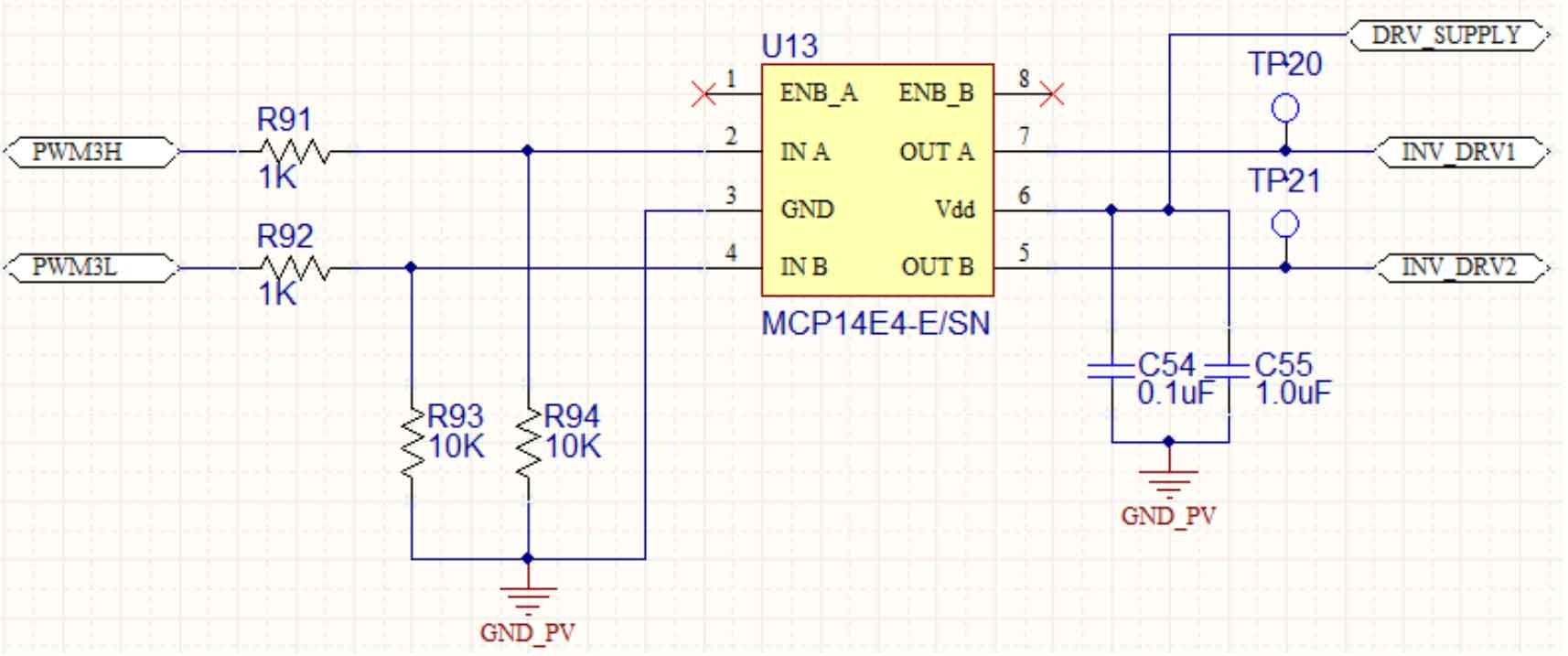
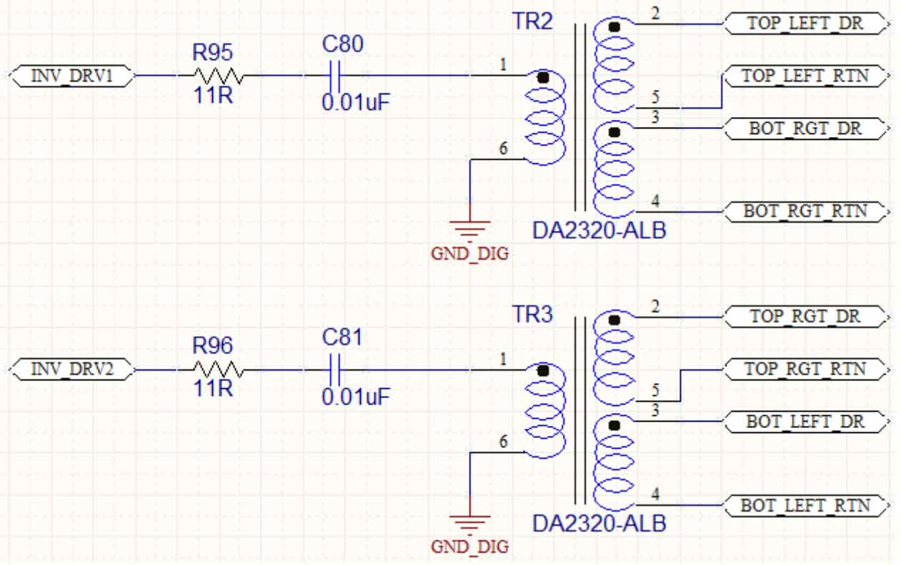
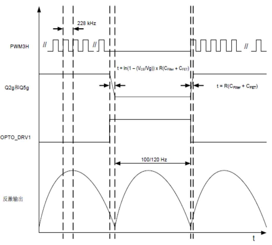
The drive transformer with a small gate is used to drive the upper and lower bridge arm MOSFETs to achieve current isolation.The gate drive transformer is driven by a high-frequency (228KHZ) PWM drive signal with a constant duty cycle.Ceramic capacitors are added in series between the gate drive transformer and the output of the drive IC to prevent saturation of the gate drive transformer.The purpose of these ceramic capacitors is to remove DC bias voltage.
The low-pass filter on the drive transformer output generates a pure DC voltage at twice the power frequency (100Hz/120Hz) to drive the full-bridge MOSFET.Since the MOSFET switches near the zero crossing point (voltage/current close to zero), this approach can reduce switching losses.The role of the optocoupler is to form a fast discharge path when the MOSFET is turned off. The pull-down resistor between the gate and source can also play the same role.The full-bridge de-folding circuit is shown in Figure 8.
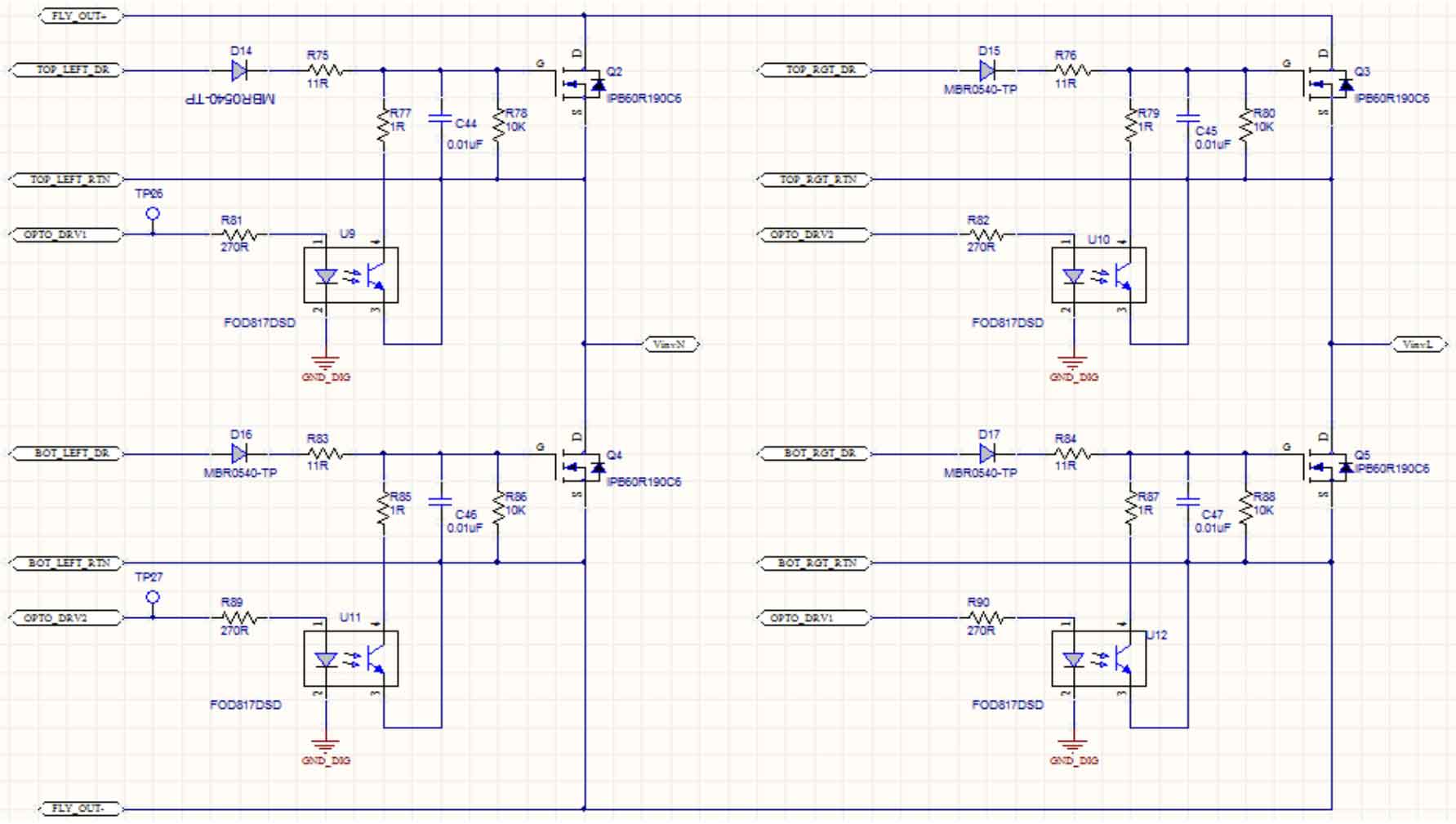
During half of the AC cycle, PWM3H switches to drive one leg of the bridge circuit.When the AC voltage approaches zero, PWM3H is disabled and the optocoupler (OPTO_DRV1) is enabled.During the other half of the cycle, PWM3L drives Q3 and Q4.The working waveform of the bridge circuit is shown in Figure 9:
4. Design of EMI filter
The electromagnetic interference (EMI) filter, consisting of a differential mode filter (C51 and L4/L7) and a common mode choke (L6), is connected to the output of the full bridge expansion circuit.The EMI filter schematic is shown in Figure 10:

5. Design of feedback network
The feedback network of solar inverters consists of the following components: solar panel voltage detection, AC voltage sensor detection, AC current sensor detection, flyback current detection, flyback output voltage detection, and zero crossing detection.
5.1 Solar panel voltage sensor
The circuit of the solar inverter after scaling factor reduction is shown in Figure 11:
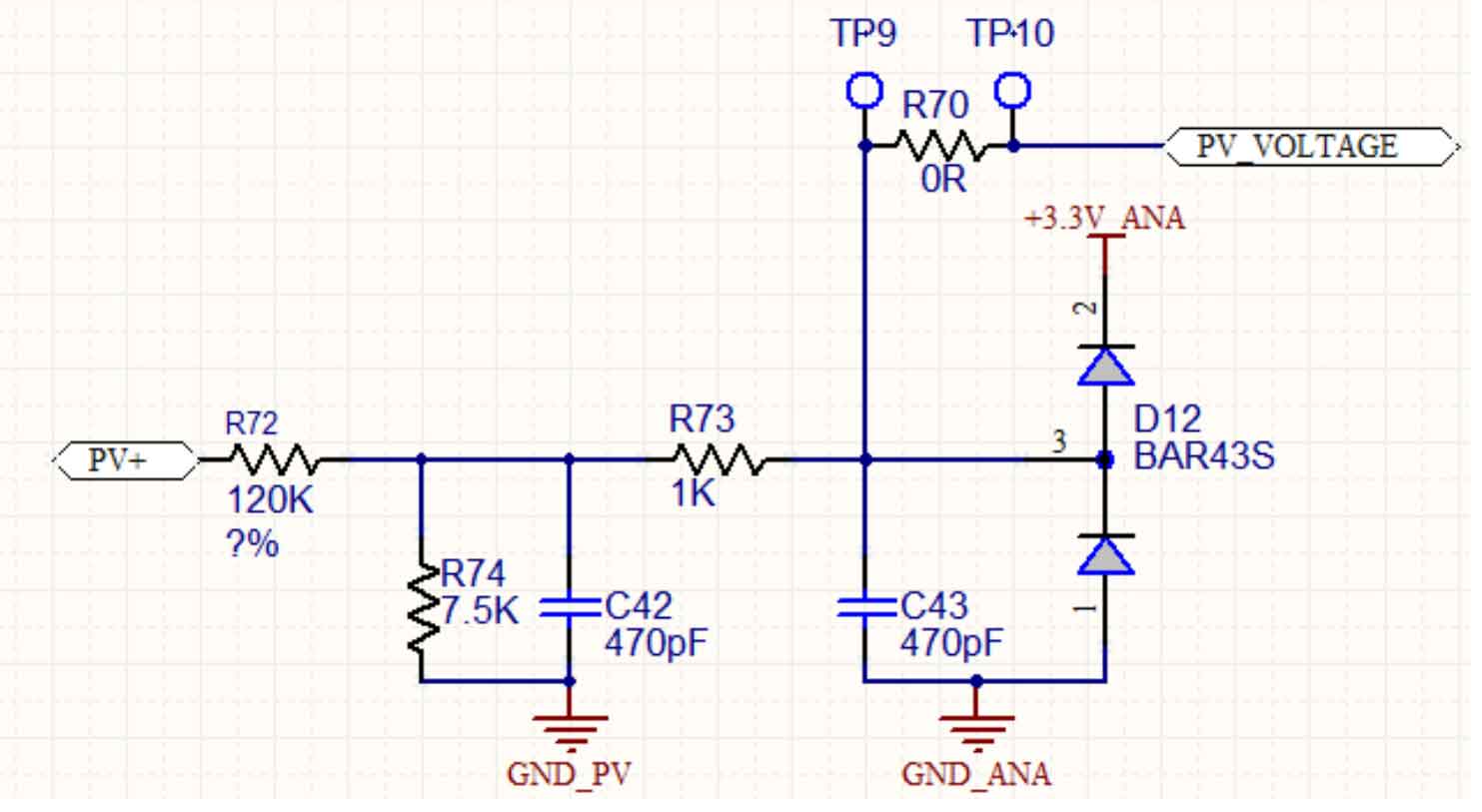
The resistive divider reduces the voltage of the solar panel to the level of the AC input voltage (0-3.3V). The formula calculates the gain of the voltage divider:

The base voltage (around 56V) is the voltage of the solar panel corresponding to the ADC pin. It is useful for accurately calculating the voltage of the ADC pin, for example, 36V on the solar panel will be equivalent to 2.11V on the ADC pin.
Resistor R73, capacitors C42 and C43 are used as additional filters.Schottky diode D12 provides protection when the voltage of the 28035 analog terminal pin exceeds 3.3V. The sensed solar panel voltage is used for maximum power point tracking, voltage feedforward compensation, and protection.
5.2 AC voltage sensor
The power frequency transformer is added to the output terminal of the micro solar inverter to maintain current isolation.The fire/zero line sensor is arranged in front of the battery interference filter output terminal to avoid affecting the function of the electromagnetic interference filter.A transient voltage suppression diode is added to the output terminal of the transformer to protect the operational amplifier and 28035 chip from transient high voltage damage.
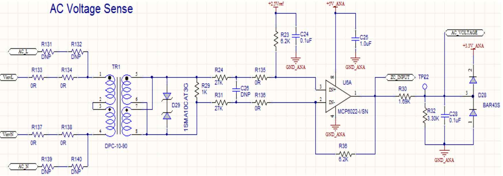
Figure 12 shows the schematic diagram of the AC voltage sensor.
The reference voltage of the AC voltage sensor is approximately 445V.The formula calculates the gain of the voltage sensor circuit:

As shown in Figure 12, a 2.5V bias voltage is added to the circuit to promote positive AC voltage.A resistive differential network is added to the circuit output to reduce the bias voltage on the 28035 to 1.65V. If necessary, capacitors C26 and resistors R135/136 can be used as low-pass filters.
5.3 AC Current Sensor
The IC output of the current sensor is fed back to the solar inverter amplifier U5 pin, and the bias voltage is fed back to the non-inverting pin.The output of the photovoltaic amplifier is amplified by a non-inverting amplifier and fed back to the analog mode of the analog-to-digital converter.The high-efficiency current signal of the 28035 analog-to-digital converter pin will have a 1.65V bias.Figure 13 shows the schematic diagram of the AC current sensor.
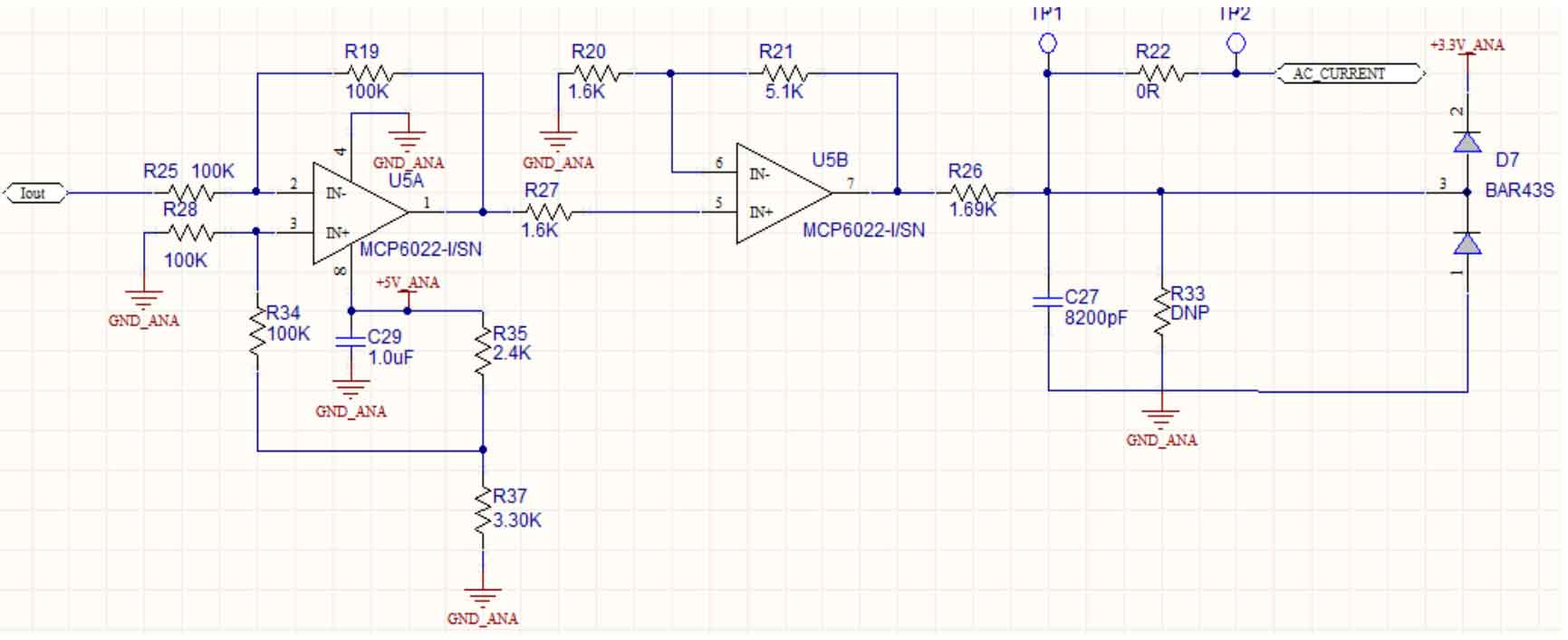
The reference current of the AC current sensor is approximately 2.14A. The gain of the current sensing circuit is calculated as follows:

5.4 Flyback Current Sensor
The current sensing transformer is used to measure the flyback current, and it is replaced by the flyback transformer and flyback MOSFET.Figure 14 shows the schematic diagram of the flyback current sensor.
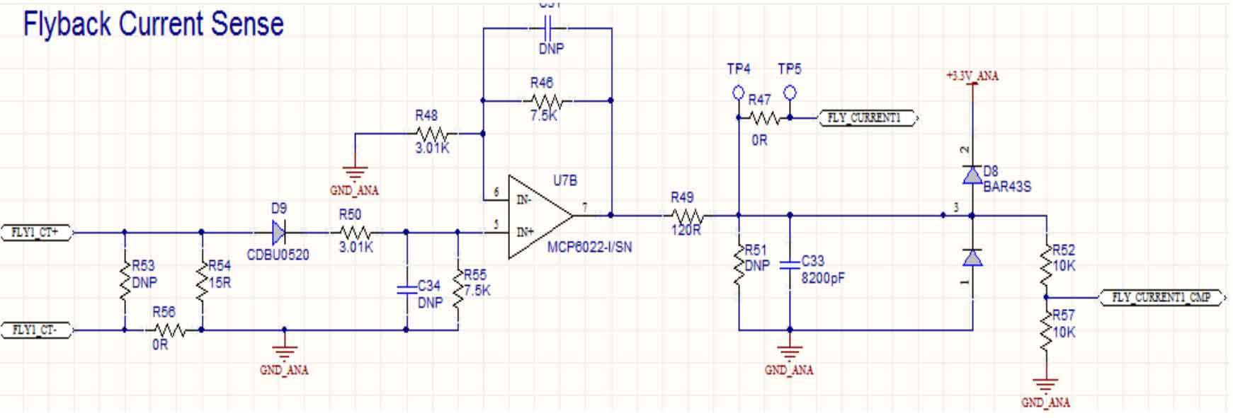
Select the current sensing transformer based on its current handling capacity, the number of turns on the secondary of the transformer, and the external load resistance.
The selection of the turn ratio and load resistance of the transformer is based on the principle of minimizing the loss of the load resistance.The peak power consumed by the load resistance can be calculated using the following formula:

A non-inverting photovoltaic amplifier with a gain of 3.5 amplifies the voltage through the load resistor as the analog-to-digital conversion voltage amplitude.A resistive differential network is added to the output of the flyback current sensor, using an on-chip analog comparator to achieve overcurrent protection.In the event of overcurrent, the PWM module will be quickly turned off. The gain value of the flyback current sensor is given by the following formula, where the single-phase reference current is approximately 13.5A.

5.5 Zero crossing detection circuit
When the grid voltage transitions from negative to positive, the state of port RB15 is changed from low level to high level, and vice versa.The output of the AC voltage differential amplifier U6.1 is compared with the relevant voltage of 2.5V by the comparator U6.2.
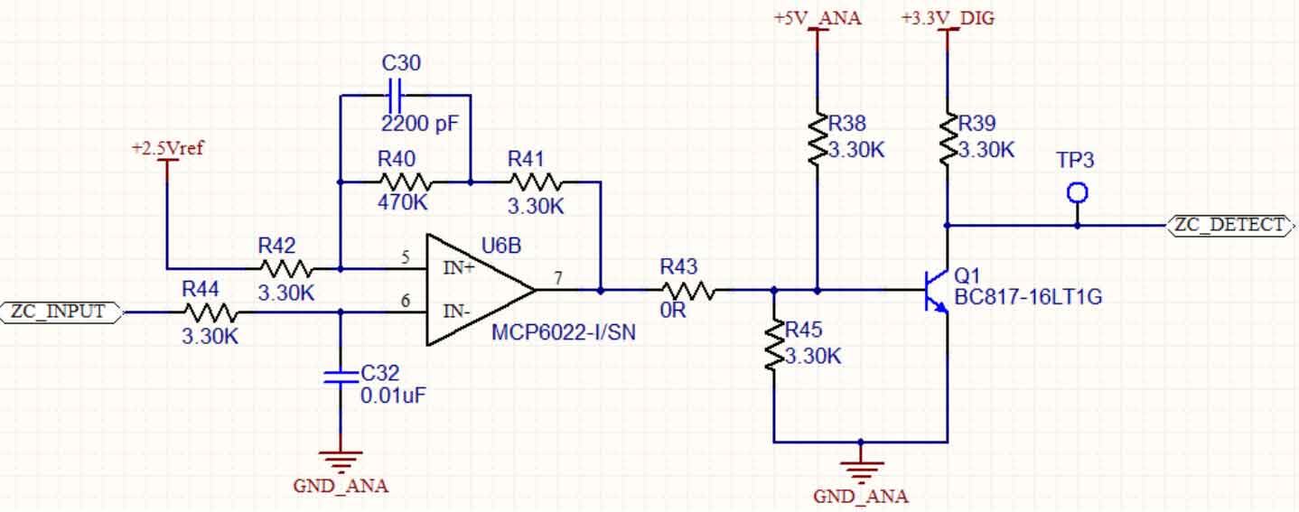
The output of the comparator drives transistor Q1, as shown in Figure 15.An AC 10mV hysteresis bandwidth is connected to the circuit through R40, R41, and C30.
5.6 Flyback overvoltage protection circuit
The output terminal of the flyback circuit is protected by a photoelectric isolation error amplifier consisting of an error amplifier, a photo-coupler, and a reference voltage to protect the micro solar inverter (to avoid catastrophic rise in output voltage of the flyback solar inverter when the secondary of the flyback transformer becomes open circuit).The flyback overvoltage protection circuit is shown in Figure 16.
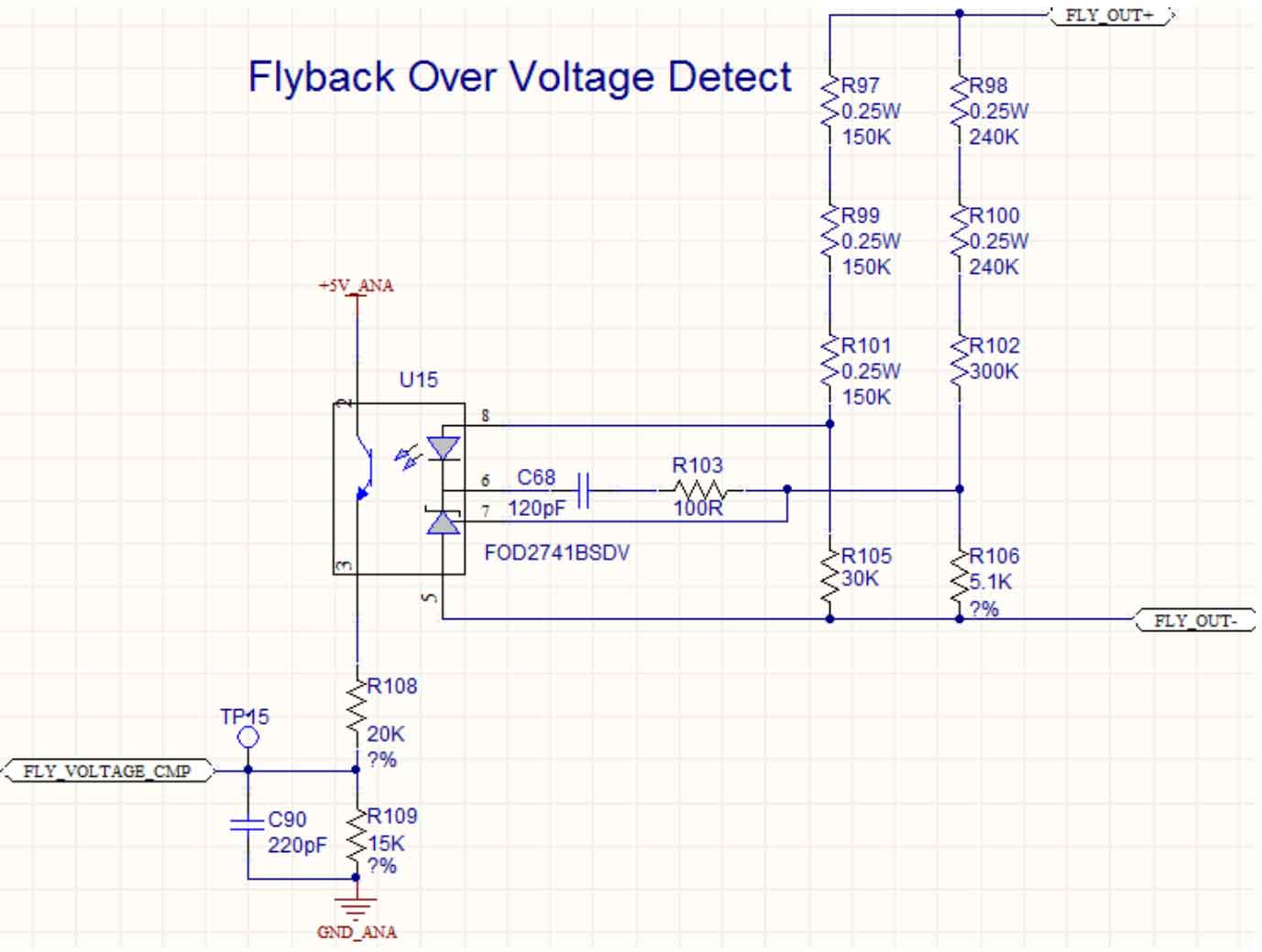
The flyback circuit will remain in the non-operational state until the voltage rises above the set limit of the maximum flyback voltage.In order to enable the optocoupler signal, the voltage of the relevant pin must be 2.5V. The formula gives the required flyback output voltage calculated to generate a voltage of 2.5V at the relevant pin:

At this time, the LED lamp will be positively biased, and the current flowing through the circuit board will be limited by the resistor network: R97, R99, R101.The maximum forward bias current carried by the LED lamp is calculated by the following equation:

At a primary current of 866uA and a minimum current transfer ratio of 100%, the current in the low-voltage or isolated portion is also 866uA.When the operating temperature of the system is 65°C, using a current transfer ratio of 60% ensures system reliability, and the current calculated for the phototransistor collector is 520uA.When the voltage at test point 15 is high, the analog comparator is interrupted, and the pulse width modulation output is disabled.
6. Summary
This article mainly introduces the hardware structure of the single-phase photovoltaic grid-connected controller: power module, interleaved flyback module, full bridge module, and feedback network module.The power module mainly provides 12V, 5V, and 3.3V driving voltages for DSP chips, gate drive ICs, and operational amplifiers, respectively.The interleaved flyback module mainly includes two parts: the selection of working modes and the design of the transformer. The working modes mainly include the following two types: continuous conduction mode (CCM) and discontinuous conduction mode (DCM).The full bridge circuit module provides a de-folding circuit for the rectified output voltage of the flyback converter.The feedback network module mainly plays a role in protecting and compensating the circuit by connecting various sensors to the main chip.