
Design the circuits of key modules in the entire portable power supply system, including FSBB charging main circuit, Buck Boost DC discharge main circuit, full bridge inverter AC discharge main circuit, power management main circuit, and sampling circuits for each module. Select appropriate chips for peripheral circuit design according to the functional requirements of each module.
1. Power management module circuit design
The hardware circuit of the power management module first selects a suitable control circuit chip, which is required to be able to quickly collect and process data from the other modules of the entire portable power system. Secondly, the output control circuit of the portable power system is designed, which can control the voltage output of the portable power system by sending signals. Finally, the data display module of the system is designed to display the operating status through the LCD screen.
1.1 Main circuit design
For embedded portable power systems, the selection of control chips is very important. Usually, the chip’s memory (ROM, RAM), main frequency, working voltage, packaging, as well as the number of GPIOs, ADCs, UART, SPI, IIC, etc. that meet peripheral requirements, as well as the actual development cost of portable power systems, manufacturer’s technical support, future requirements, and compatibility issues should be considered. Taking all factors into consideration, the portable power supply system chooses the 32-bit ARM STM32F103C8T6 microcontroller as the main control chip.
| Name | Parameter |
| Core processor | 32-bit ARM Cortex-M3 |
| CPU speed | 72MHz |
| FLASH | 64KB × 8bit |
| SRAM | 20KB × 8bit |
| GPIO | PA0-PA15, PB0-PB15, PC13-PC15, PD0-PD1 |
| ADC | Two 12bit ADCs with a total of 12 channels |
| Interface type | SPI, IIC, CAN, UART |
| Working voltage | 2V~3.6V |
The table above explains the main technical parameters of this chip, which has a high-performance control core, a CPU processing speed of 72MHz, a total of 48 pins, including 2 12 bit range ADCs, a total of 12 channels, 2 SPI interfaces, 3 UARTs, 2 IICs, and one CAN. This single chip has a small size and complete functions, meeting all expected control requirements of portable power systems.
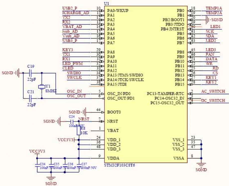
The circuit diagram of the main control chip is shown in Figure 1, with pins 5 and 6 externally connected to an 8MHz crystal oscillator, pins 2 and 4 used as switch signals for DC-DC and DC-AC, pins 11 detecting output current, pins 14 detecting battery voltage, pins 15 and 16 detecting USB output current and voltage, and pins 21, 22, 25, and 26 controlling the LCD screen to display data.
1.2 Output Control Design of Portable Power Supply System
If the portable power supply system operates without load for a long time, it will cause battery loss, so it is particularly important to design the discharge control part of the portable power supply system. Since the discharge module of the portable power supply system is provided with input voltage by the lithium battery pack, it is only necessary to control the output of the battery voltage to each module to control whether the portable power supply system discharges. Usually, in the switching circuit of DC-DC converters and DC-AC converters, Design using the conduction characteristics of N-MOS and P-MOS transistors.
1.2.1 DC output control design
As shown in Figure 2, a DC switch circuit is composed of Q11’s P-MOS transistor and Q12’s N-MOS transistor. The gate of the N-MOS transistor is connected to the DC switch control signal (DC_switch), the source is connected to the ground, the drain is connected to the gate of the P-MOS transistor, the source of the P-MOS transistor is connected to the battery output, and the drain is connected to the downstream control circuit. When the microcontroller outputs a high level control signal to the DC switch, the N-MOS transistor conducts current from the drain to the source. At this time, the gate voltage of the P-MOS transistor is pulled down, and the gate source voltage of the P-MOS transistor is negative. Therefore, the P-MOS transistor will conduct and output battery voltage to the Buck Boost circuit for power supply.

1.2.2 Design of AC output control
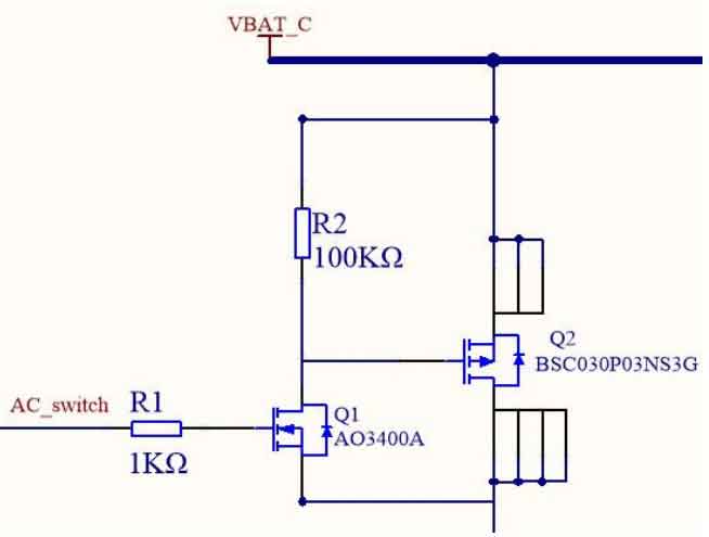
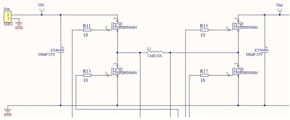
As shown in Figure 3, similar to the design concept of DC output control, the AC switch circuit is composed of Q3’s P-MOS transistor and Q1’s N-MOS transistor circuit. When the microcontroller gives the AC switch control signal (AC_switch) a high level, the battery voltage will be output to the DC-AC circuit for power supply.
1.3 Data Display Circuit Design
The data display module displays the current operating status of the portable power supply system in real time. Users can intuitively see the remaining power, output voltage, output power, interface working status, etc. of the portable power supply system through the LCD screen, which is an important part of portable power supply system management. In microcontrollers with microcontrollers as the core, segmented LCD screens with appropriate driver chips are widely used in various portable mobile devices due to their ultra-low power consumption characteristics. The HT1621 driver chip, which is widely used, is selected for display circuit design in portable power systems.
HT1621 is a 128 mode memory mapped LCD driver with multiple functions. The S/W configuration characteristics of HT1621 enable it to match various LCD applications. The internal structure of HT1621 is shown in Figure 4.
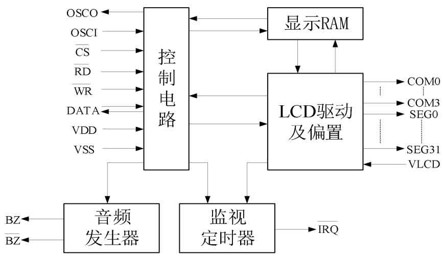
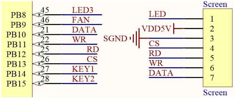
The static display memory RAM of the driver is composed of 32-bit continuous address units, with memory addresses corresponding to pins SEG0-SEG31 from 0 to 31, and any RAM unit containing 4 bits corresponds to COM0-COM4, so the driver can display up to 128 bits of data information. Connect the CS, RD, WR, and DATA pins to the STM32 chip, as shown in Figure 5. The data displayed in the RAM can be directly mapped to the LCD driver unit, and then accessed through the operation code to control the data display of the LCD screen.
2. Charging module circuit design
According to the requirements analysis of the charging module and the research on control strategies in Chapter 3, the charging circuit is designed using the FSBB topology structure. After inputting voltage within the specified range, the FSBB circuit can stably output a DC voltage of 12.6V to charge the lithium battery pack.
As shown in Figure 6, after the input voltage passes through the filtering circuit of the electrolytic capacitor, the DC power is transmitted to the FSBB circuit structure composed of four N-MOS transistors, one inductor, and one capacitor. After the four MOS transistors are controlled by the driving signal to continuously conduct and turn off, a stable 12.6V DC power is output and transmitted to the lithium battery pack for charging.
2.1 Design of absorption circuit parameters
In actual circuit design, due to the parasitic inductance generated by the leads, an LC oscillation circuit is formed with the parasitic capacitance in the MOSFET. Additionally, due to the presence of multiple frequency components in the driving signal waveform, a series resonance circuit is formed at the same or similar resonant frequencies. So, when designing a circuit, a resistor (R11, R12, R13, R14) is usually connected in series at the gate of the MOSFET to quickly attenuate oscillations by reducing the Q value, preventing circuit failures. However, the series resistance should not be too large, otherwise it will slow down the opening and closing time of the MOS transistor, increase losses. After experimental debugging, the final selection of the series resistance is 10 Ω.
2.2 Output capacitor selection
The output capacitor C is used to filter the output voltage, allowing the FSBB converter to output DC smoothly. The size of the selected capacitor value is mainly determined by the ripple requirements of the output voltage, which is determined by the following equation:

Among them, Δ Vo is the output voltage ripple, Δ IL is the inductor current ripple, Fs is the PWM operating frequency, ESR is the equivalent series inductance of the output capacitor, and capacitors with low ESR should be selected as much as possible during the design process. Through calculation and testing, an electrolytic capacitor with a capacitance value of 100uF was selected. Due to the highest operating voltage value of 12.6V in the FSBB circuit, the capacitor withstand voltage value should be higher than the highest voltage during normal operation and a certain margin should be retained. To ensure the performance of the portable power supply system, this article selects a capacitor with a withstand voltage value of 25V.
2.3 Inductance selection
To ensure the stability of the FSBB circuit loop, the inductance value is usually selected at 2.2 μ H~10 μ Between H, high sensitivity value 4.7 μ H~10 μ H is usually suitable for circuits with large input and output voltage differences, such as 5V to 20V; Low sensitivity value 2.2 μ H is suitable for circuits with similar input and output voltages but high currents. After experimental debugging, the final inductance selected was 2.2 μ H.
3. Discharge module circuit design
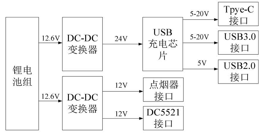
According to the requirements analysis of the discharge module in Chapter 2, the circuit design in this section is divided into two modules: DC output and AC output. The DC discharge module uses the battery voltage to boost or reduce the battery voltage by 12.6V through a DC-DC converter, and outputs it to the USB charging chip or directly connects to the output port; The AC discharge module outputs 220V AC power to the load by passing the battery voltage through the front stage push-pull boost circuit and the rear stage full bridge inverter circuit.
3.1 Design of DC discharge circuit
The portable power supply system DC discharge module is designed based on commonly used charging interface requirements: as shown in Figure 7, the lithium battery pack voltage outputs a stable 12V DC power through a DC-DC converter to supply the cigarette lighter and DC5521 interface; At the same time, the lithium battery pack outputs 24V DC power to the USB charging chip through a DC-DC converter, and then provides corresponding power requirements for interfaces of different charging protocols through the USB charging chip.
3.1.1 Main circuit design
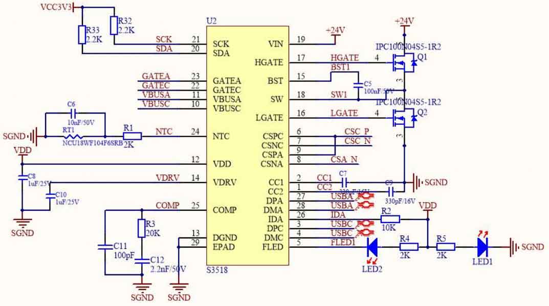
The DC discharge module includes two DC-DC converters. Considering the voltage range of the lithium battery pack is between 8.6-12.6V, one needs to be boosted to 24V to power the USB charging chip, and the other needs to provide a stable DC voltage of 12V to the output interface. According to the functional introduction of the DC-DC topology in Chapter 3, the selected DC-DC converter chip is the EG1164 chip produced by Yijing Microelectronics.
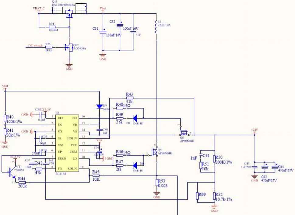
The EG1164 chip is a high-voltage and high current Buck Boost synchronous rectification power management chip that integrates reference power supply, oscillator, error amplifier, cycle by cycle current limiting control, half bridge drive and other functions to meet design requirements. Figure 8 shows the hardware circuit diagram of using the EG1164 chip to increase the battery voltage to 24V.
The output voltage of EG1164 is determined by two voltage divider resistors on the FB pin and an internal error amplifier reference determined by voltage, as shown in Figure 9.
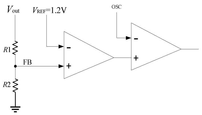
The reference voltage of this module is 1.2 V, and the formula for setting the output voltage is:

This section requires an output voltage of 24V. In Figure 8, R50, R52, and R99 resistors are selected as 200K, 11K, and 200K. When outputting DC power to the cigarette lighter and DC5521 interface, it is required to convert DC-DC to 12V, and only the voltage divider resistor on the FB pin needs to be modified.
3.1.2 USB charging module circuit design
USB is a bus architecture developed by Inter Corporation, which specifies a universal serial interface standard. With the continuous improvement of technology, the USB protocol has evolved from being only used for data transmission to now supporting multiple USB fast charging protocols for charging different devices.
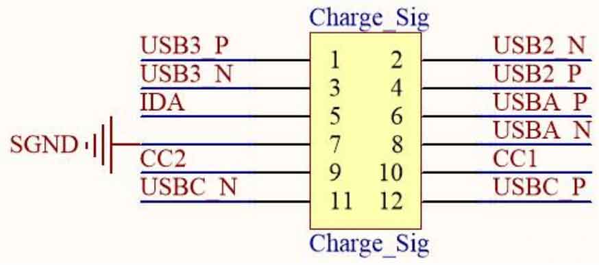
In response to the USB output interface requirements of portable power systems, the SW3518 and SW3521 chips produced by Zhuhai Zhirong Technology Company were selected for design. Type-C, USB3.0, and two USB2.0 interfaces were provided for the output interface. Figure 10 shows the USB interface design diagram.
(1) SW3521 peripheral circuit design
SW3521 is a chip that meets multiple fast charging protocols and supports dual port simultaneous charging. It has high integration and complete functions. It is equipped with an efficient synchronous buck converter, and only a small number of peripheral devices are needed to meet the requirements of various charging schemes. Figure 11 is designed using SW3521 USB 2.0 interface circuit.
Pin 1 of the chip receives 24V voltage output from the Buck Boost circuit as the input voltage of the chip, while pins 6 and 7 receive DP and DM signals from the USB2.0 interface.
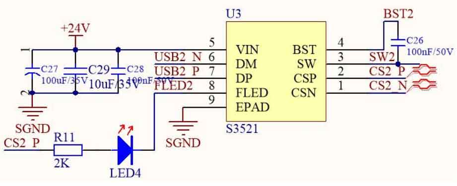
(2) SW3518 peripheral circuit design
Unlike the SW3521 chip, SW3518 can support fast charging output of A+C dual port and any port simultaneously, and can ensure independent current limiting of a single port. In terms of step-down converters, the current limiting is increased from 3.5A to 5A, resulting in a higher output current. And it supports the PD fast charging protocol, meeting the design requirements. Figure 12 shows the Type-C and USB3.0 interface circuit designed using SW3518.
The pins 17 and 19 of the chip receive 24V voltage output by the Buck Boost circuit as the input voltage of the chip and the driving voltage of the MOS transistor; The pins 1, 2, 3, and 4 of the chip receive CC1, CC2, DP, and DM signals from the Type-C interface; The chips 26, 27, and 28 receive IDA, DP, and DM signals from the USB3.0 interface. Unlike the USB2.0 protocol, in addition to two DP and DM data lines providing differential data, the Tpye-C interface uses configuration pins CC1 and CC2 to avoid conflicts with the DP and DM pins, ensuring that the USB PD protocol does not affect data transmission while transmitting electricity.
3.2 AC discharge circuit design
3.2.1 Push-pull Boost Main Circuit Design
The AC discharge module converts the low DC voltage stored in the lithium battery into a high DC voltage through a boost circuit, and then uses an inverter circuit to convert the high DC voltage into AC voltage output. In this article, the EG1612 chip produced by Yijing Microelectronics Co., Ltd. is selected as the boost circuit. It integrates three high-voltage half bridge drivers and can output two 40kHz to 111kHz PWM signals in push-pull mode. It also provides protection functions such as undervoltage shutdown, overvoltage shutdown, and circuit overcurrent shutdown. When a fault occurs, the buzzer can be used to give an alarm in a timely manner, and the voltage input can be turned off to prevent damage to circuit components caused by excessive voltage and current. The product has complete functions and a small model, as shown in the above performance, which meets the design requirements. The hardware circuit diagram of EG1612 is shown in Figure 13.
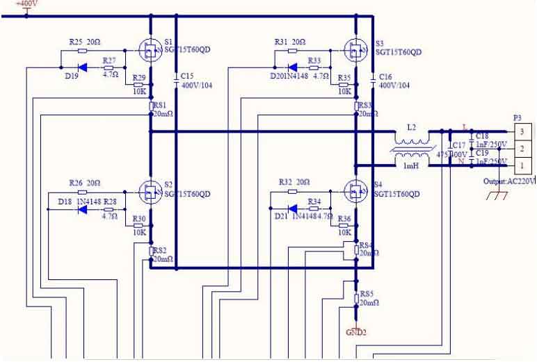
3.2.2 Full bridge inverter main circuit design
The STC12C5410AD chip is selected as the main control chip for the full bridge inverter circuit. The 400V DC high voltage output by the front stage push-pull boost is used as the input voltage of the rear stage inverter circuit. The SPWM wave is generated by the STC microcontroller to control the inverter bridge composed of four IGBTs S1-S4, outputting a pulse sequence with sinusoidal patterns. After being filtered by capacitors and inductors, a stable AC 220V voltage is output and transmitted to the load, Figure 14 shows the hardware circuit design of the rear inverter.
4. Sampling circuit design for portable power supply system
The sampling circuit of the portable power supply system mainly collects current signals and voltage signals. On the one hand, it is transmitted as feedback signals to the control circuits of each module to complete self adjustment, and on the other hand, it is transmitted to the control circuits of the power management module for data processing. The status information is displayed on the LCD screen. As the control chip selected for the portable power supply system can only collect voltage information within the range of 0-3.3V, if it exceeds this range, It can cause damage to the control chip, therefore, selecting a reasonable sampling circuit is essential in the circuit design of portable power systems.
4.1 Operational amplifier sampling circuit
An operational amplifier is an electronic device with two voltage signal input terminals and one voltage signal output terminal group. It usually uses an operational amplifier and other devices such as resistors, capacitors, and inductors to form an operational amplifier circuit. It can perform a series of basic operations on analog signals in the circuit, such as addition and subtraction, multiplication and division, proportional operation, differential operation, and integral operation, to achieve the function of signal conditioning, The main function of operational amplifiers in portable power systems is to sample voltage and current.
4.1.1 Voltage sampling circuit
Due to the fact that the AD channel of the control chip can only collect the voltage range of 0-3.3V, and the voltage in the circuit is often higher than this range, voltage sampling is required. In this section, a proportional operation amplification circuit is designed to collect voltage, as shown in Figure 15.
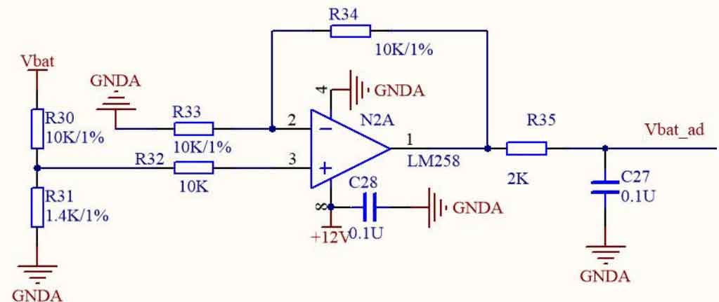
Operational amplifiers have two characteristics at the input end, namely virtual break and virtual break. By utilizing these characteristics, it can be derived that the following equation:

By substituting the resistance value, we obtain:

Microcontroller processing Vbat_ The value of the ad signal can be used to obtain the value of the battery voltage Vbat.
4.1.2 Current sampling circuit
Due to the inability of the control chip to directly collect current, it is necessary to design a circuit to convert the current into voltage information and transmit it to the control chip. There are two commonly used circuit designs, one is an addition and subtraction operation circuit, and the other is a low edge detection amplification circuit.
The first method is to add a sampling resistor between the in-phase and inverse ends of the operational amplifier, and obtain the current value by collecting the ratio of the voltage difference between the two ends to the sampling resistor, as shown in Figure 16.
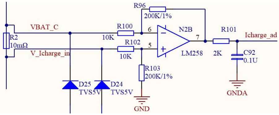
Among them, the battery charging current Icharge is:
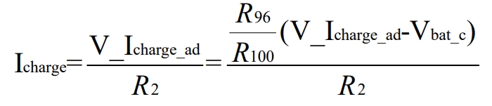
Substitute the resistance value into:

The second method is to fully utilize the virtual break characteristic of the operational amplifier. When collecting the charging current provided to the USB in the DC output module, as the charging current almost completely passes through the sampling resistor end, a low side detection circuit can be used for design, as shown in Figure 17.
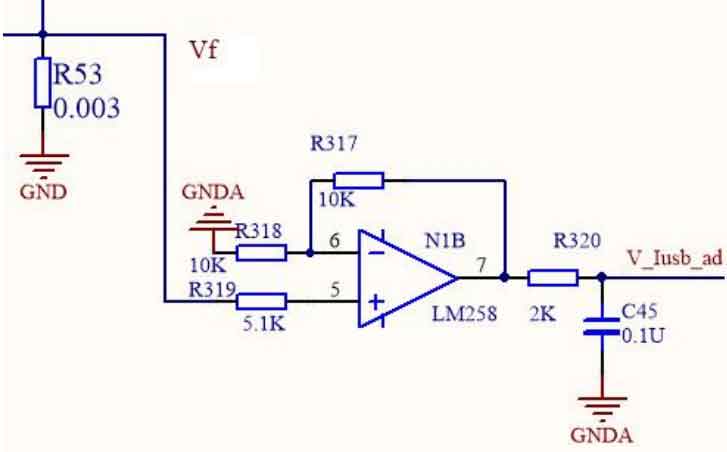
Among them, the USB charging current IUSB is:

Substitute the resistance value into:

4.2 Optocoupler isolation sampling circuit
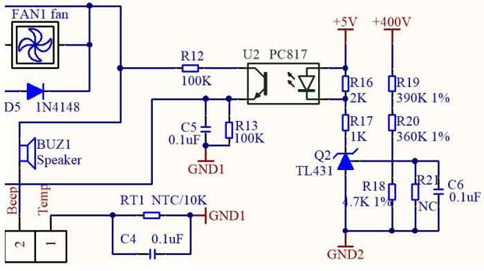
The optocoupler isolation circuit achieves single-phase signal transmission. By completely isolating the input signal and output signal of the control circuit, the anti-interference ability of the portable power system is enhanced, ensuring the stability of the circuit while also increasing its service life. The DC-AC front-end sampling circuit adopts optocoupler isolation sampling. The optocoupler isolation sampling circuit mainly collects the boosted DC voltage. When the voltage reaches 400V, the fan is turned on to prevent excessive temperature. As shown in Figure 18, when the DC voltage reaches 400V, the photodiode starts to work, emitting enough light to turn on the phototransistor, and the phototransistor starts to work, turning on the fan.
4.3 Current Transformer Sampling Circuit
In power supply circuits, there may be differences of more than ten orders of magnitude in the magnitude of current or voltage. Due to the high voltage in the circuit, it is not suitable for direct measurement and requires conversion measurement. A current transformer is a device that converts large current into small current based on the principle of electromagnetic induction. It is commonly used in circuits that detect alternating current. It is composed of a closed iron core and winding, and often connects the secondary with fewer turns in series into the tested circuit. As shown in Figure 19, in the DC-AC front-end circuit, the current transformer receives the AC power output by the transformer, and the secondary output AC voltage is rectified by a rectifier bridge composed of D10, D11, D12, and D13, and then transmitted to the control chip for current feedback information.
5. Summary
According to the requirements of the portable power supply system, suitable control chips and peripheral circuit devices were selected. The key circuit designs of each module in the portable power supply system were introduced in detail, and the schematic design was carried out based on principles such as signal integrity. The modules were combined as a whole from a physical perspective.