The designed household photovoltaic inverter mainly utilizes the high-performance K60 to control it. Firstly, the input and output voltage and current of the entire system are collected through the AD acquisition module. Then, a series of filtering processes are performed on the collected parameters through K60. Finally, the digital PID algorithm is used to calculate the duty cycle of the PWM wave. In order to ensure the normal and stable operation of the system, many protection circuits have been added to improve the adaptability of the system.
1. System technical conditions
The main design indicators of this design are shown in the table:
| Number | Technical indicators | Requirement |
| 1 | Power level | 1kW |
| 2 | MPPT range | 80V~500V |
| 3 | Intermediate DC voltage | 400V |
| 4 | Output voltage effective value | 220VAC ± 5% |
| 5 | Output voltage frequency | 50Hz ± 4% |
| 6 | Output current waveform THD | ≤ 5% |
| 7 | Output voltage waveform THD | ≤ 5% |
| 8 | Inverter efficiency | >90% |
2. Control circuit design
The core of control is the Kinetis series microcontroller from Freescale, which means “fast”. The Kinetics series microcontroller adopts Freescale 90 nanometer thin film memory (TFS) flash technology and Flex memory function (configurable embedded EEPROM), with a maximum of 10 million erasures. The Kinetics microcontroller series integrates the latest low-power innovative technology.
Has broad interconnectivity, secure peripherals, and human-machine interfaces. There are five types: K10, K20, K30, K40, and K60.
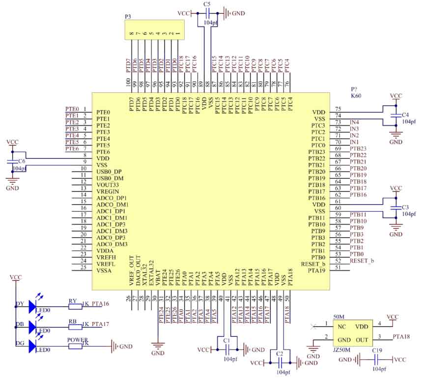
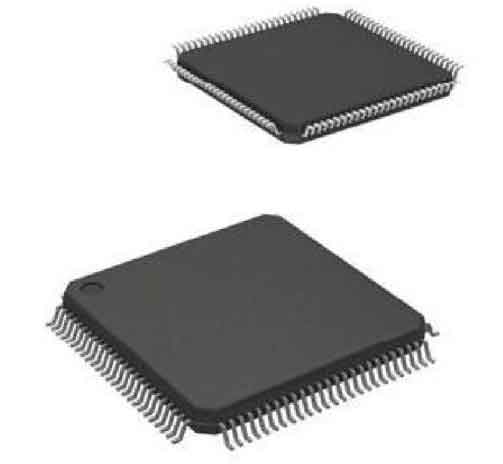
The chip used for the controller is a 100 pin K60 (MK60DN512VLL100) provided by Freescale, as shown in Figure 1. In order to ensure high working stability of the microcontroller, a reliable minimum system board was designed and sent to a specialized circuit board manufacturer for processing, as shown in Figure 2.
2.1 Design of Microcontroller Power Supply
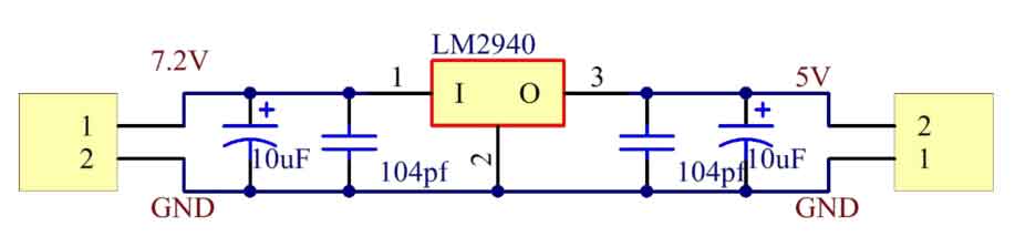
A stable system requires a reliable power supply to support it, which is crucial for the normal operation of the control system. Therefore, when designing the control circuit of solar inverters, it is necessary to configure stable and suitable power sources for each functional module to ensure the stable operation of the entire system. At present, there are two commonly used low-voltage DC power supplies: switch type regulated power supplies such as LM2575 and LM2596, and series type linear regulated power supplies such as 7805 and LM2940. LM2940 is a low-voltage differential positive voltage three terminal regulator with a fixed output voltage; Output voltage 5V; Output current 1A; When the output current reaches 1A, the input and output voltage drop shall not exceed 0.8V; Maximum input voltage 26V; Working temperature -40~+125 ℃; There is a static current reduction circuit inside; Current limitation; Overheat protection; Battery reverse connection protection circuit; Reverse insertion protection circuit. The disadvantage is low efficiency and high power consumption. After conducting experiments on some voltage stabilizing power modules, the selected voltage stabilizing chip is LM2940. The circuit is shown in Figure 3:
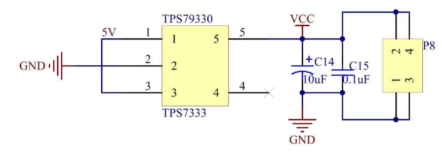
The power supply voltage of the K60 microcontroller is 3.3V, and the working current is not large. However, since the AD reference voltage of the microcontroller is directly taken from the power supply end of the microcontroller, it is necessary to ensure that the microcontroller power supply has good stability and small fluctuations, otherwise it will directly affect the acquisition of analog signals by the microcontroller ADC. In order to further enhance stability, the K60 microcontroller uses TPS79333 to further reduce voltage and stabilize voltage on the basis of 5V. The circuit diagram is shown in Figure 4:
2.2 Design of 5V power supply for the main control board
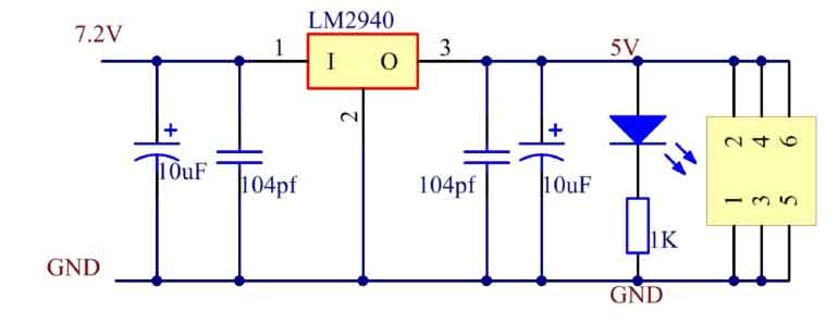
Except for the microcontroller, all other components that require 5V power supply are powered by the main control board’s 5V power supply. This part of the power supply is powered by a 2940 chip, which is led out by a pin to facilitate the insertion and removal of power cables for various components. The schematic diagram is shown in Figure 5.
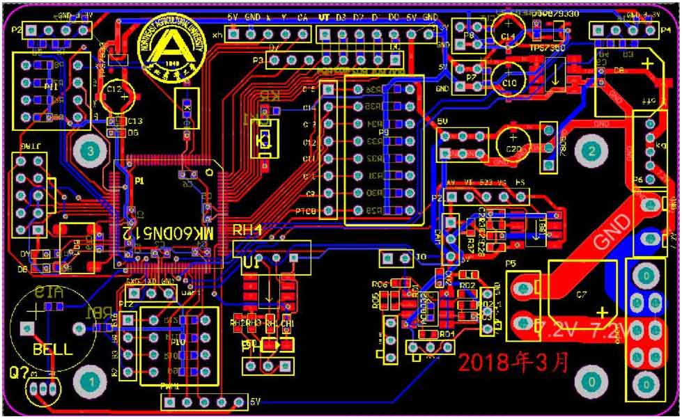
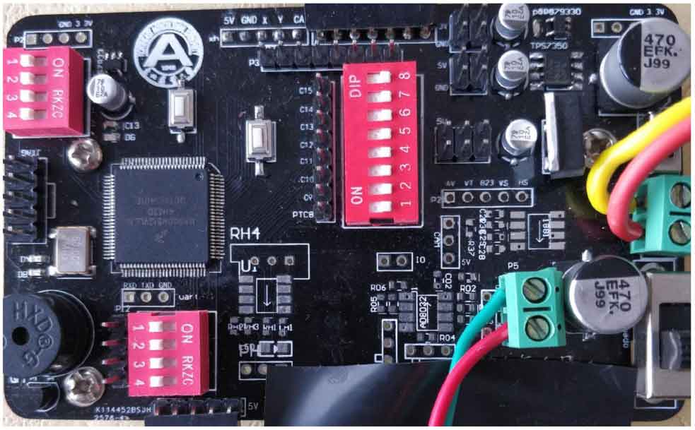
Use Altium Designer14 software to draw the schematic and PCB diagram of the K60 minimum system board, send it to the manufacturer for PCB sampling, and manually solder and debug the circuit board after processing. The PCB wiring diagram and physical diagram are shown in Figures 6 and 7, respectively.