
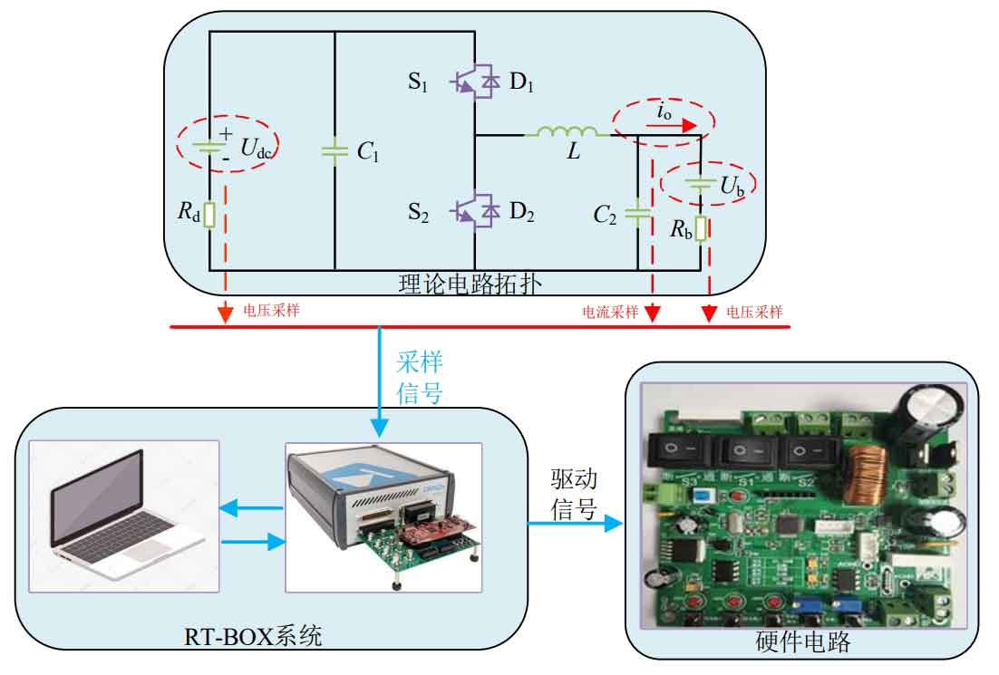
Experimental verification will be conducted on the control performance of the composite frequency division coordinated control strategy in the off grid state through the semi physical platform RT Box (a simulator equipped with analog and digital input/output channels for power electronics applications, utilizing real-time hardware in the loop (HIL) testing and a universal processing unit for rapid control prototypes). At the same time, this article establishes a 5kW energy storage grid connection experimental platform to verify the charging and discharging status between the energy storage system and the power grid.
1.Experimental parameter settings
1.1 DC-DC parameter design
Design indicators: It can work in charge and discharge mode, with a switching frequency of 20kHz, a high-voltage side voltage of 48V, a voltage ripple of 4%, and a maximum current of 2A.
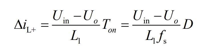
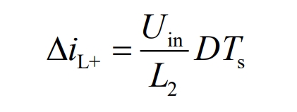
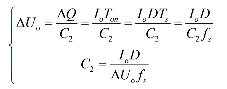
1) Design of main circuit inductance and capacitance parameters in Buck mode: The increase in current of the inductance current in a continuous state Δ IL+is shown in equation 1:
In the equation:
Δ IL+- increase in inductance current;
Uin – input side voltage;
Uo – output side voltage;
Ton – Switching tube conduction time;
Fs – Switching frequency.
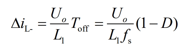
When the inductance current is in continuous operation, the reduction of inductance current Δ IL is shown in Equation 2:
In the equation:
Δ IL – reduction of inductance current;
Toff – switch tube closing time;
D – Duty cycle of switch tube;
L1- Output side inductance.
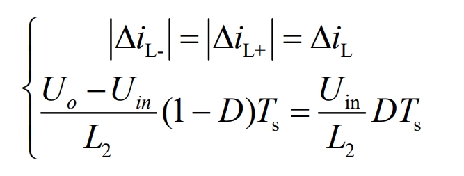
In the balanced state of the circuit, as the inductance does not consume energy, the relationship between inductance increment and inductance decrement is shown in Equation 3:
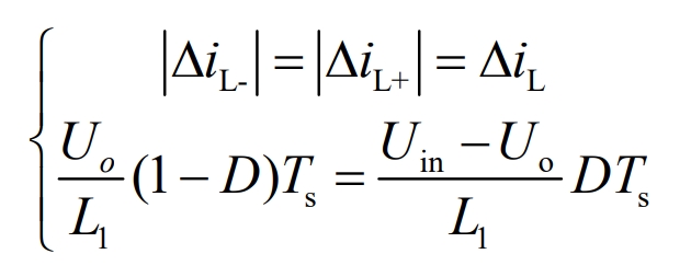
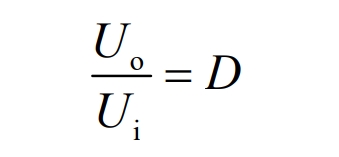
The relationship between input and output voltage and duty cycle can be obtained as shown in Equation 4:
The total charge amount of a capacitor in one cycle Δ Q is shown in equation 5:
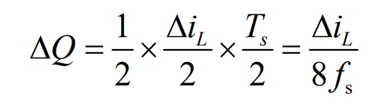
In the equation:
Δ Q – Amount of charge.
Output Voltage Ripple Δ Uo is shown in equation 6:
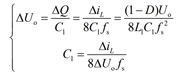
In the equation:
Δ Uo – voltage ripple, with a ripple voltage of 4%;
The critical inductance value when the inductive current is critically continuous is shown in Equation 7:
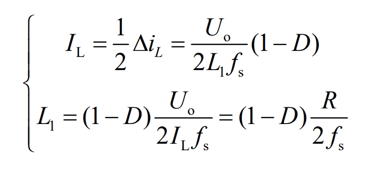
In the equation:
IL – output current;
2) Design of main circuit inductance and capacitance parameters in Boost mode:
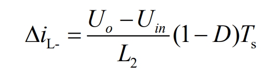
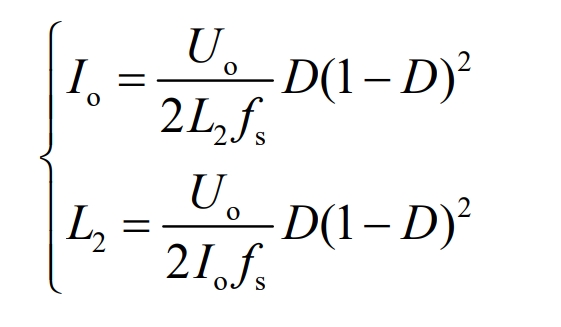
The increase in inductance current when it is in a continuous state Δ IL+is shown in equation 8:
Inductive current reduction Δ IL – As shown in Equation 9:
In the balanced state of the circuit, as the inductance does not consume energy, the inductance increment is equal to the inductance decrement relationship, as shown in Equation 10:
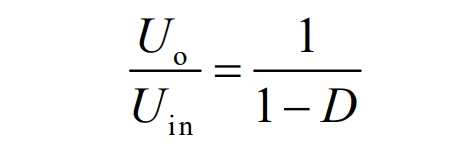
The relationship between input and output voltage and duty cycle can be obtained as shown in Equation 11:
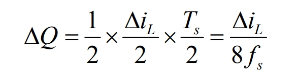
The total charge of a capacitor in one cycle Δ Q is shown in Equation 12:
Output Voltage Ripple Δ Uo is shown in Equation 13:
The average load current and inductance value at critical continuous inductance current are shown in Equation 14:
In the equation:
Io – average load current;
Considering the inductance threshold, the inductance L is selected as 700 μ H. Capacitors C1 and C2 are selected as 1000uF.
1.2 DC-DC Circuit Design
The main circuit topology of the bidirectional Buck/Boost converter is shown in Figure 1.
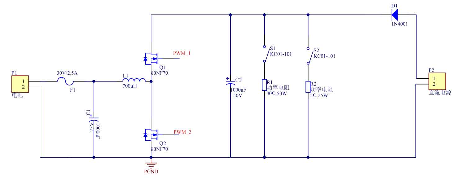
The driving pulse frequency of the two switches in the bidirectional half bridge converter is 20kHz. MOS tube VGS=10V. The driving circuit is designed based on the half bridge driver chip IR2104. The chip has three types of logic as inputs: 3.3V, 5V, and 15V. The driving voltage of the switch is between 10V and 20V. The on dead time and off dead time inside the chip are 680nS and 150nS, respectively, to avoid direct short circuits between the upper and lower transistors. The meanings of each pin of the half bridge driver chip IR2104 are shown in Table 1.
| Pin code | Function Description |
| IN | The logic input of the high and low voltage gate driver outputs (HO and LO), which are in phase with HO and in phase with LO |
| SD | Used to turn off logic input |
| Vb | High voltage side floating power supply |
| HO | High voltage side gate drive output |
| Vs | High voltage side floating power supply circuit |
| Vcc | Low voltage side and logic fixed power supply |
| LO | Low voltage side gate drive output |
| COM | Low voltage side common point |
The application circuit of IR2104 is shown in Figure 2.
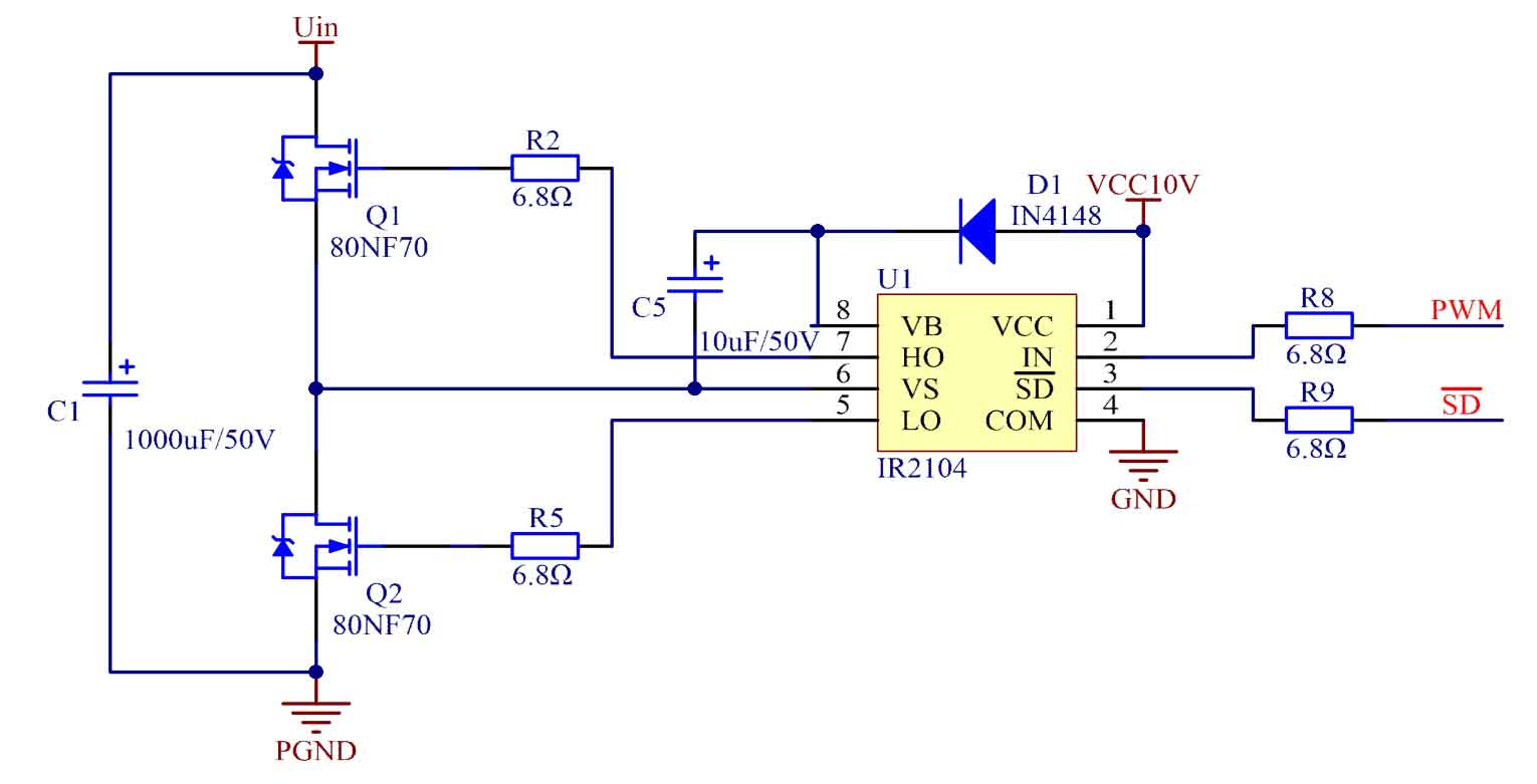
The chip drives the high-voltage side MOS transistor of the half bridge circuit through the charge pump bootstrap function. When the input side is powered on, the input power is charged to capacitor C5 through a high-speed diode, and the voltage charged to the positive pole becomes 10V. If the state of two MOS tubes is that the upper tube is off and the lower tube is on, the negative voltage of C5 becomes common ground. When the PWM level output by the main control chip flips, the HO pin and LO pin of IR2104 output opposite pulse levels. The lower switch transistor is cut off, the upper switch transistor is on, the negative voltage of C5 increases to the input voltage that needs to be controlled Uin, and the positive voltage of C5 is clamped to Uin+10V, because the presence of a diode will protect the power VCC from damage. Capacitor C5 supplies power to the chip pin HO, resulting in a high-voltage MOS gate source voltage VGS of 10V. PWM driving level flipping causes the upper and lower switch tubes to alternately conduct.
The PWM driving signal generated by the driving chip is shown in Figure 3.
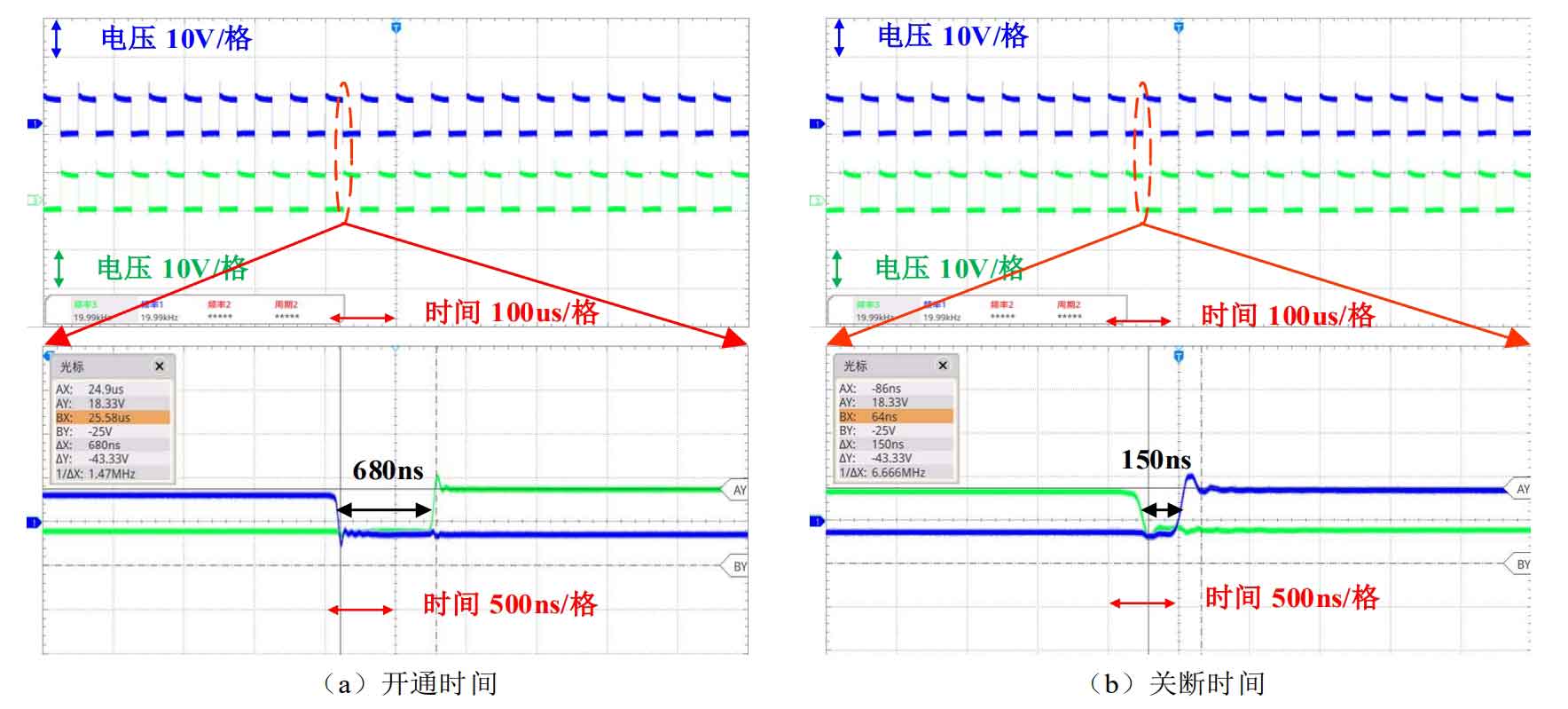
From Figure 3, it can be seen that the opening dead time of the driving waveform is 680ns, and the closing dead time is 150ns.
2. Hardware circuit design and analysis
2.1 Design of DC-DC control module
Utilize the RT Box upper computer as the control system. Connect the sampling circuit to the analog input port, output the driving signal of the switch tube through RT Box, and connect the driving signal to the hardware circuit of the main circuit and the driving circuit. By controlling the simulation interface of the PLECS upper computer interface, the opening and closing of the main circuit switch tube can be controlled. The experimental verification can be completed in the loop using the hardware of the experimental platform.
2.2 Design of DC-DC sampling circuit
1) Voltage sampling
The circuit used for voltage measurement is shown in Figure 4.
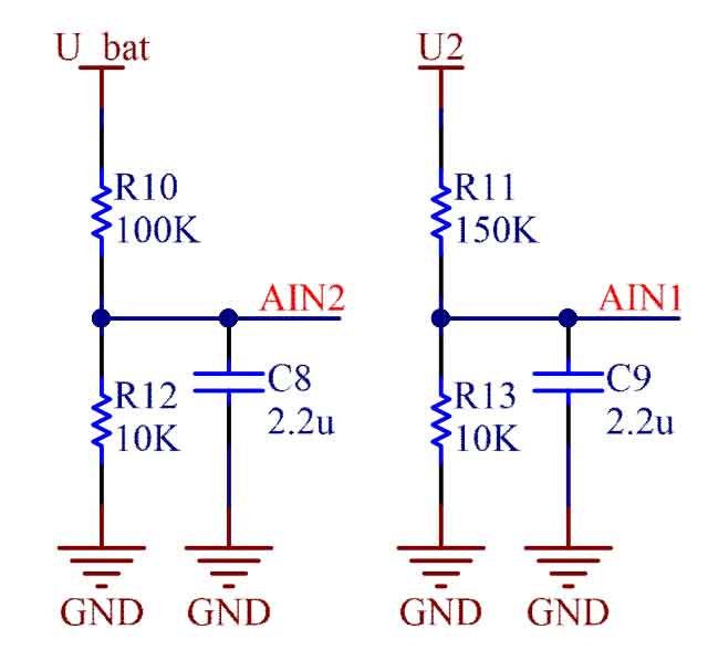
Voltage sampling is achieved through a voltage divider resistor, connected in parallel at the input end in 2.2 μ F capacitance to reduce voltage ripple.
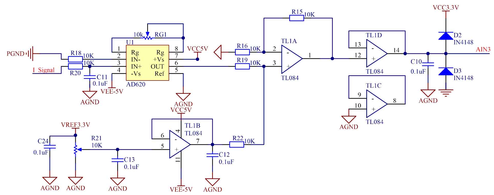
2) Current sampling
The current sampling circuit is shown in Figure 5.
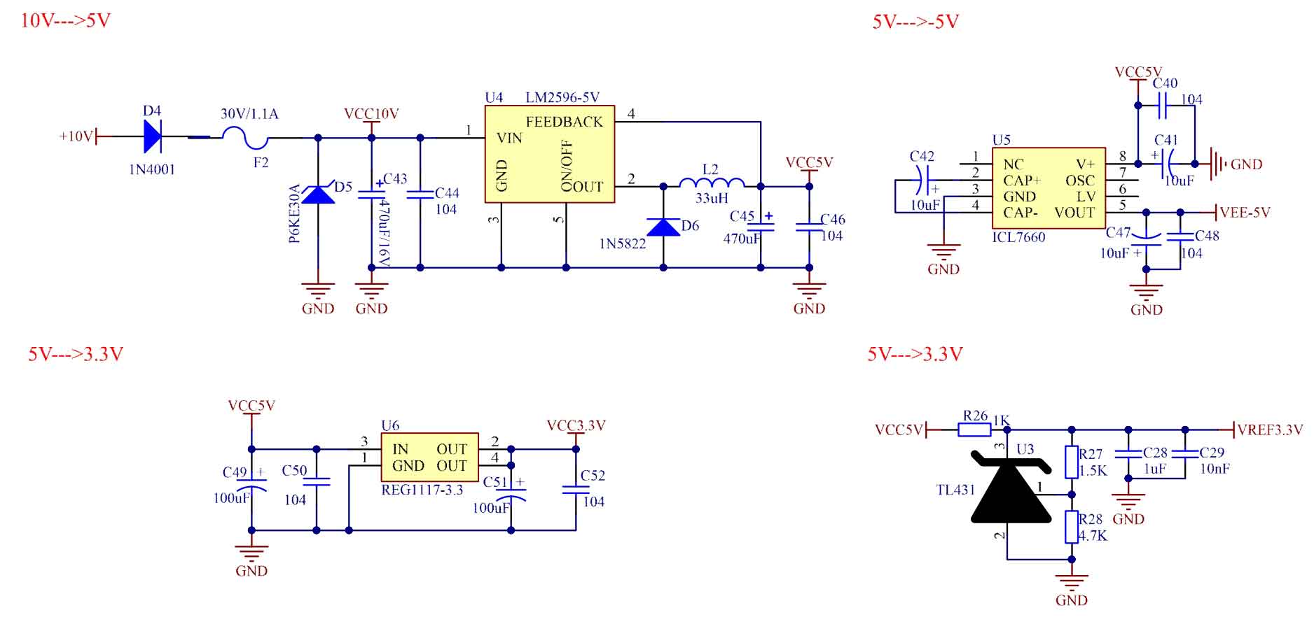
2.3 DC-DC auxiliary circuit design
The auxiliary circuit of the bidirectional DC-DC converter has four voltage levels of 10V, 5V, 3.3V, and -5V, as shown in Figure 6.
3. Experimental platform
1) Experimental platform 1: The bidirectional energy storage converter experimental platform is shown in Figure 7.
The experimental platform in Figure 7 mainly includes five modules: power module, main circuit module, sampling module, energy storage module, and load module.
2) Experimental platform 2: The energy storage charging and discharging experimental platform is shown in Figure 8.
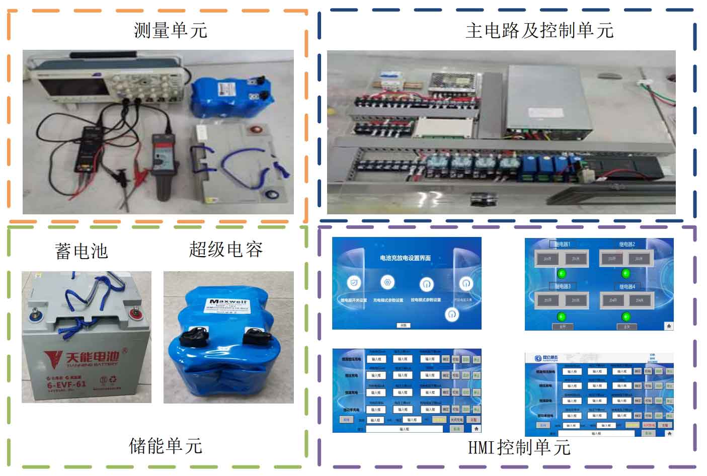
The experimental platform in Figure 8 mainly includes five modules: measurement, power supply, main circuit, sampling, energy storage, and load.
4. Experimental results and analysis
1) Experimental waveform of bidirectional DC-DC energy storage converter
Load jump occurs at 0.25 seconds, 0.5 seconds, 0.75 seconds, and 1 second respectively.
(1) The driving waveform of the energy storage converter is shown in Figure 9.
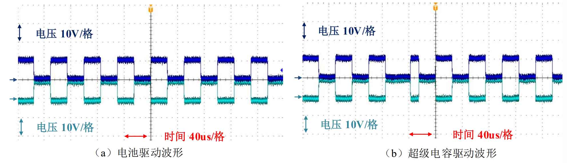
Figure 9 (a) shows the driving waveform of the converter connected to the battery, and Figure 9 (b) shows the driving waveform of the converter connected to the supercapacitor.
The comparison of experimental waveforms between traditional control strategy and composite frequency division coordinated control strategy is as follows:
(2) The current waveform of the supercapacitor and battery is shown in Figure 10.
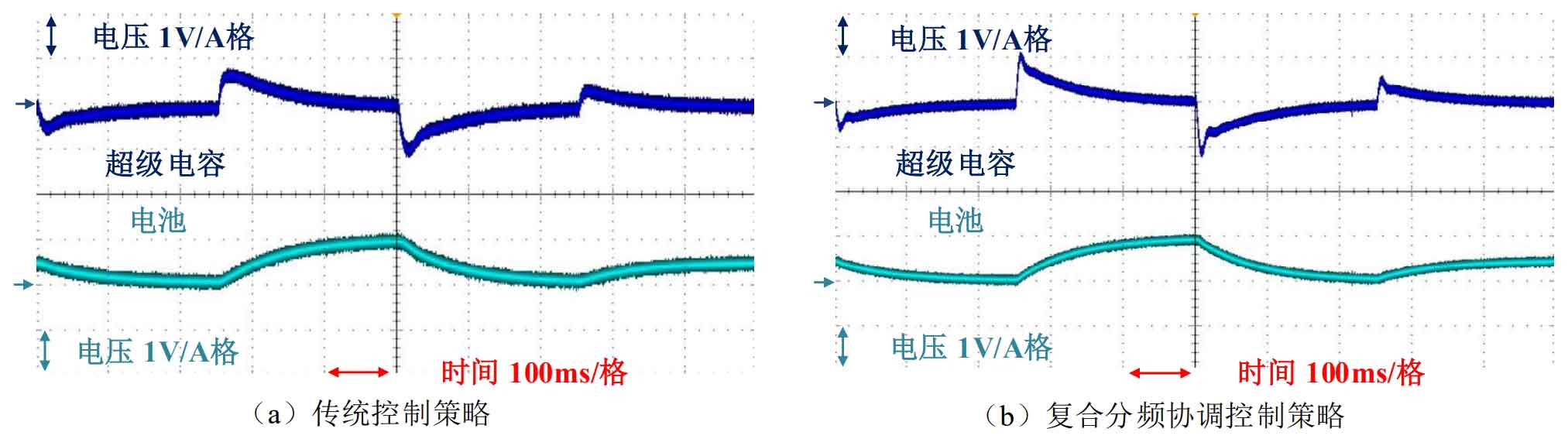
Figure 10 (a) shows the current waveforms of the traditional control strategy battery and supercapacitor, while Figure 10 (b) shows the current waveforms of the composite frequency division coordinated control strategy battery and supercapacitor. From the above figure, it can be seen that when the load suddenly changes, the supercapacitor can quickly respond to high-frequency signals caused by transient processes, while the battery responds to low-frequency signals.
(3) The DC bus voltage for load loading and load shedding is shown in Figure 11.
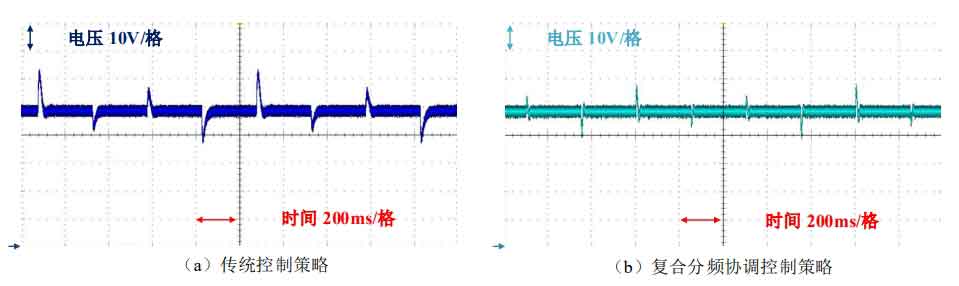
Figure 11 (a) shows the distribution control strategy DC bus voltage waveform, and Figure 11 (b) shows the composite frequency division coordinated control strategy DC bus voltage waveform. Through comparison, it can be seen that the control strategy proposed in this article can effectively reduce the peak pulse of DC bus voltage and the fast recovery time of the system.
(4) The amplitude of the DC bus voltage waveform under load shedding is shown in Figure 12.
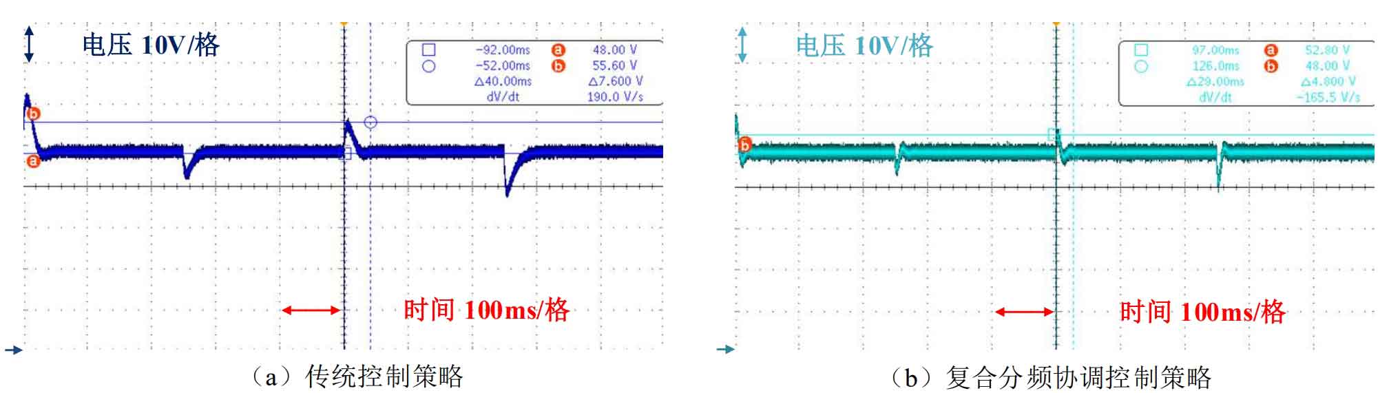
Figure 12 (a) shows the waveform of traditional control strategy DC bus voltage load shedding, and Figure 12 (b) shows the waveform of composite frequency division coordinated control strategy DC bus voltage load shedding. From the above figure, it can be seen that the peak voltage fluctuation of the traditional control strategy during load shedding is 55.6V, and the bus voltage recovery time is 40ms. The voltage fluctuation peak of the control strategy proposed in this article is 52.8V, and the bus voltage recovery time is 29ms. Through comparison, it was found that the control strategy proposed in this article reduced the peak voltage from 15.8% to 10% and the response time by 27.5% in the load shedding state.
(5) The amplitude of the DC bus voltage waveform under load is shown in Figure 13.
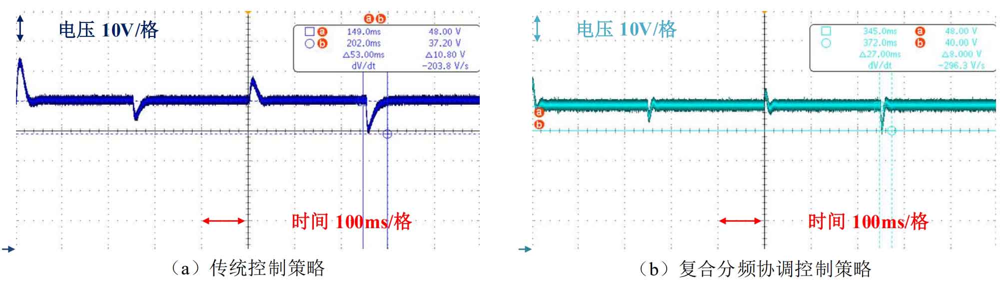
Figure 13 (a) shows the DC bus voltage loading waveform of the frequency division control strategy, and Figure 5-13 (b) shows the DC bus voltage loading waveform of the composite frequency division coordination control strategy. From the above figure, it can be seen that the traditional control strategy has a peak load voltage fluctuation of 58.8V and a bus voltage recovery time of 53ms. The voltage fluctuation peak of the control strategy proposed in this article is 56V, and the bus voltage recovery time is 27ms. Through comparison, it was found that the control strategy proposed in this article reduced the peak voltage from 22.5% to 16.6% in the loading state, and the response time was approximately reduced by 49%.
(6) Energy storage charging and discharging experimental waveform
The waveform of the battery charging experiment is shown in Figure 14.
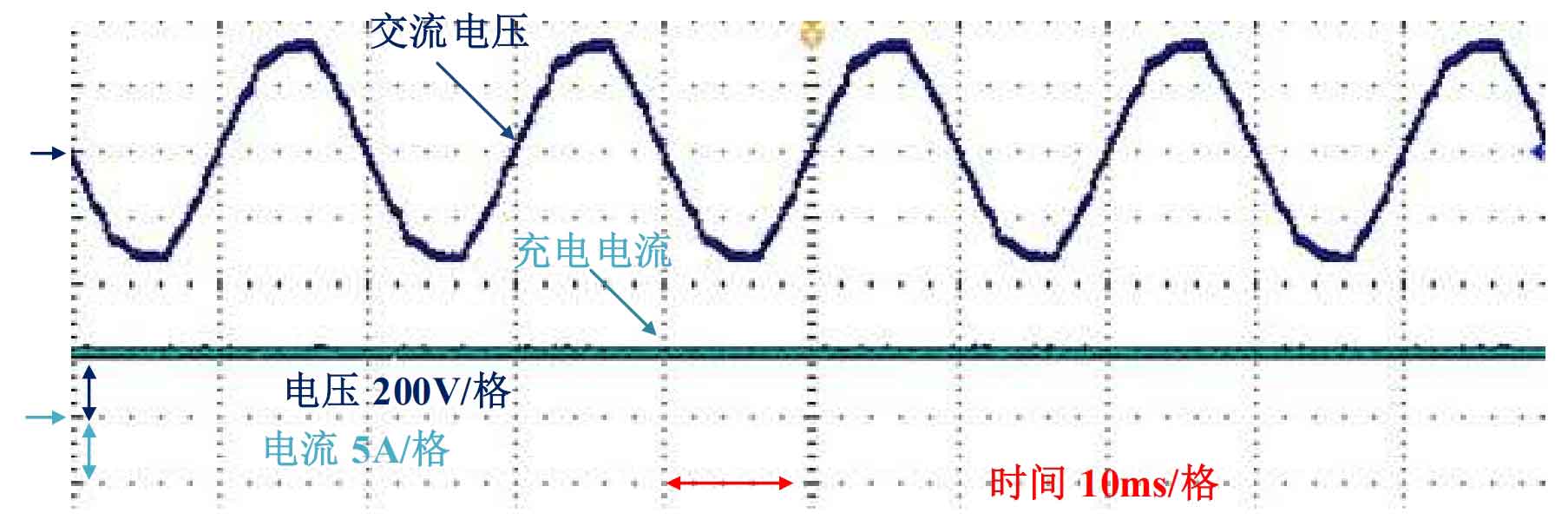
From the above figure, it can be seen that the power grid charges the battery with a charging current of 5A.
(7) The waveform of the energy storage system grid connection experiment is shown in Figure 15.
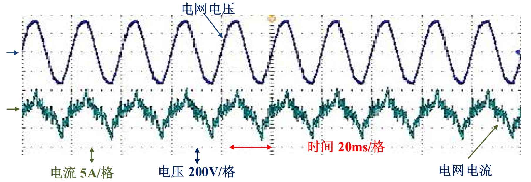
From Figure 15, it can be seen that the battery releases energy to the power grid, and the energy storage system is in a discharge state. The voltage and current of the power grid are in phase, and the power grid absorbs energy.
5. Summary of this chapter
Firstly, design the experimental parameters and hardware circuit of the bidirectional Buck/Boost energy storage transformer. The composite frequency division coordinated control strategy was experimentally validated under off grid conditions using the RT Box platform, and the experimental results showed the effectiveness of the proposed control strategy. Finally, a 5kW energy storage converter system was built to verify the energy conversion between the energy storage system and the power grid.
With the vigorous development of renewable energy and its increasing proportion in the energy system, the combination of renewable energy and energy storage systems will bring continuous driving force to new energy. By optimizing the installed capacity and energy storage configuration capacity of photovoltaics, the occurrence of wind and light abandonment can be greatly reduced, and the development cost of the system can be reduced. Effective control of bidirectional Buck/Boost energy storage converters can suppress the impact of renewable energy power fluctuations and high-power load fluctuations on bus voltage.
(1) Mathematical modeling of photovoltaic microgrid systems with energy storage systems, power and loss calculations of photovoltaic cells, mathematical analysis of the charging and discharging states of batteries and supercapacitors, and ideal switching mathematical modeling of Buck/Boost converters. This serves as a theoretical foundation for the capacity optimization calculation of the optical storage system in Chapter 3 of this article and the composite frequency division coordination control strategy in Chapter 4.
(2) Determine multi-objective functions based on economy, energy surplus rate, and complex charge loss rate, and allocate capacity through particle swarm optimization algorithm combined with constraint conditions. Indicating that a reasonable installed capacity can reduce the cost of the system while reducing the rate of load loss and energy surplus, and adaptive capacity matching can be carried out based on different weight coefficients.
(3) Utilizing energy storage systems to compensate for system power errors and utilizing the advantages of hybrid energy storage for power allocation, i.e. utilizing supercapacitors and batteries to respond to high-frequency and low-frequency signals respectively. To further increase the use of supercapacitors and improve the dynamic performance of the system, using supercapacitors to compensate for low-frequency signal errors in order to improve the performance of supercapacitors, At the same time, an open-loop controller was added to increase the system’s speed, forming a composite frequency division coordinated control strategy. Finally, simulation and comparative analysis were conducted in the system’s offline state to verify the feasibility of the composite frequency division coordinated control strategy.
(4) The experimental verification of the energy storage system in the off grid state was conducted using the RT Box semi physical platform. The experimental results showed that the proposed control strategy reduced the peak voltage from 15.8% to 10% and the response time by 27.5% in the off grid state. In the loading state, the peak voltage is reduced from 22.5% to 16.6%, and the response time is reduced by 49%. Finally, the energy exchange between the energy storage system and the power grid was verified through the 5kW energy storage converter experimental platform.