
In order to further test the performance of the two-stage inverter structure proposed in this article, this chapter continues to explore the hardware implementation method of the inverter system, and proposes the precautions to be taken in the circuit design process based on the characteristics of the circuit.
For the convenience of debugging and design, the entire system is divided into three parts: the main control circuit, measurement circuit, and inverter circuit. The main control circuit is responsible for outputting driving signals and performing data conversion. The measurement circuit is mainly responsible for collecting voltage and current data. The inverter circuit is designed separately based on the switching frequency, and the two-stage circuit is used together to complete the inverter work.
STM32 generates PWM signals to control the bus and midpoint voltage in a closed-loop manner. At the same time, it outputs corresponding PWM signals based on the voltage parameters of the front-end circuit to drive the back-end solar inverter. After passing through an LC filter, the DC power supply is finally converted into three-phase sinusoidal AC power, and the three-phase pure resistive load is connected in a Y-shaped manner. For safety reasons, the hardware circuit design power did not reach the simulated design power. The physical circuit design has a single-phase voltage effective value of 88 V, a current effective value of 4.4 A, and a total power of 1.1 kW, powered by two 150 V DC power sources.
1. Main control circuit
The main control unit uses the STM32F103 series VBT6 produced by STM Semiconductor. This microcontroller adopts a high-performance ARM-CORTEX-M3 architecture, which has the advantages of high speed and low power consumption. The operating frequency can reach 72 MHz. The main control circuit is the smallest system formed by the core of this chip and the addition of basic peripheral equipment.
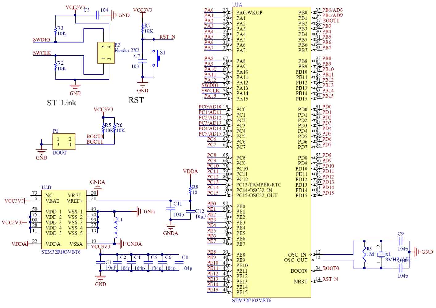
This system is a simple microcontroller minimum system, mainly consisting of a microcontroller, ST Link downloader interface, reset button, BOOT startup mode, indicator light, power supply, crystal oscillator and other basic peripheral devices. The system designed in this article also includes a voltage follower for use by the ADC input port.
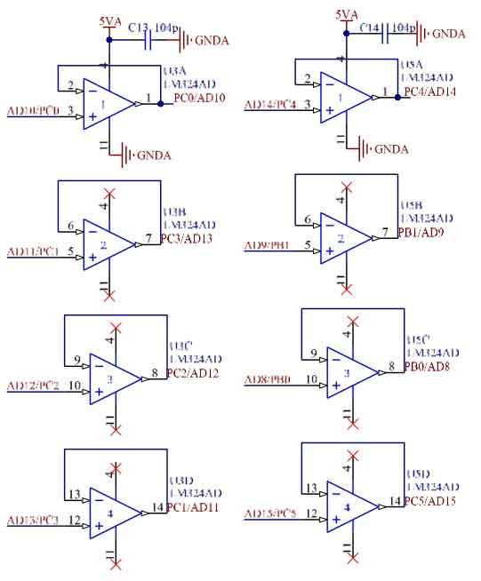
Based on work experience, in power electronic work environments with high-power switching power supplies, it is necessary to add a voltage follower at the input of the ADC to increase input impedance, reduce the impact on the front-end, and prevent ADC input voltage oscillation. If there is no voltage follower, it is easy to experience oscillations, causing the ADC to be unable to collect stable data. This article uses two LM324 four channel integrated operational amplifiers to provide voltage followers for eight ADC input ports.
2. Measurement circuit
Due to the fact that this system is a closed-loop control system, it is necessary to collect real-time dynamic indicators and provide feedback to the microcontroller. The main data collected includes the voltage and current conditions at various points during operation.
2.1 Voltage measurement
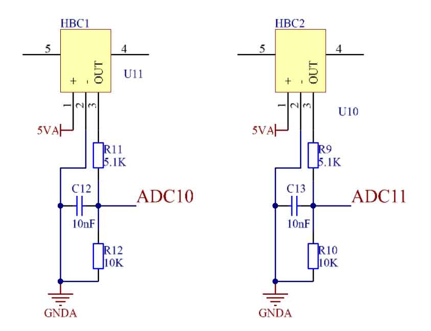
The voltage measurement methods used in this article mainly include differential voltage measurement, voltage transformers, and Hall voltage sensors. The schematic diagram of the differential voltage measurement circuit is shown in Figure 3:
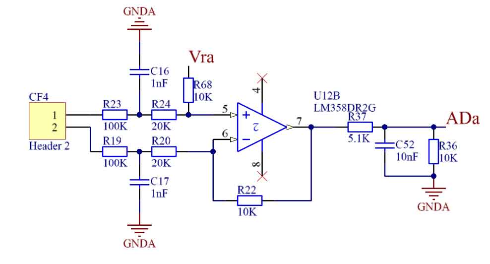
Differential voltage measurement mainly includes two differential amplification circuits. For example, in the upper part, 𝑅 1, different resistance values can be set to change the potential of the positive input terminal of the operational amplifier, adjust the output terminal of the operational amplifier, and flexibly configure different ranges. Based on the principle of minimum path, LM358 dual integrated operational amplifier is selected as the operational amplifier for these two differential voltage measurements. The differential voltage measurement circuit is mainly used for measuring DC voltage. The DC voltage that needs to be measured in this system is the bus voltage VPN and midpoint voltage VMN of the front-end voltage regulation circuit. In addition, a Hall voltage sensor measurement circuit is also used.
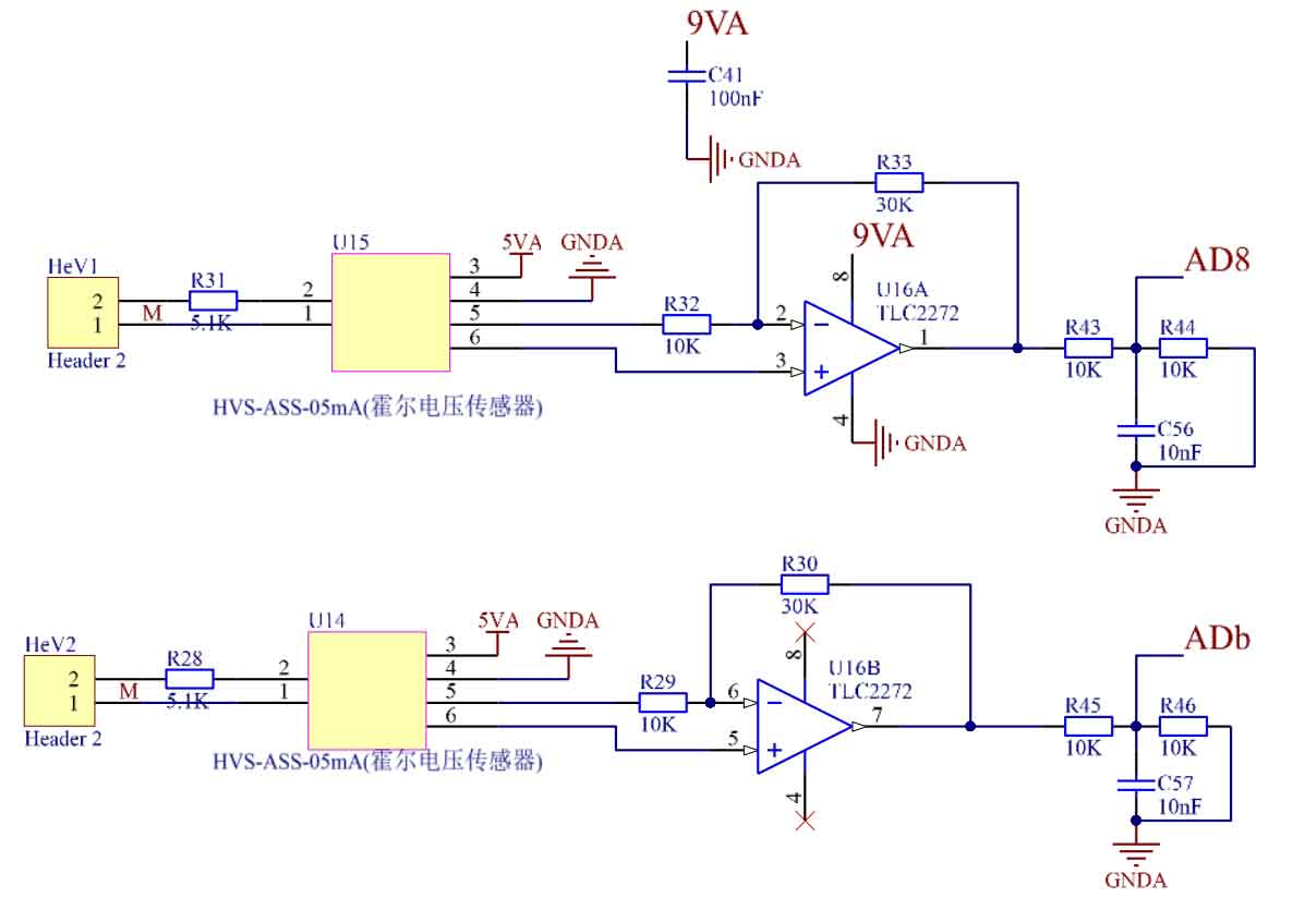
The working principle of Hall voltage sensors is based on the Hall effect, and a closed-loop Hall voltage sensor is selected. It can measure the voltage values of AC, DC, and various waveforms under electrical isolation. The positive and negative input terminals of the sensor are connected to the measured port through a series current limiting resistor. The sensor adopts a+5V analog power supply, and there is also an AC voltage transformer measurement scheme.
A voltage transformer can be seen as a small voltage regulator, mainly composed of an iron core, primary coil, secondary coil, and wiring terminals. The primary coil is connected to the AC voltage system circuit, while the secondary coil is connected in parallel to the measuring instrument or relay protection device, and it is required that the secondary coil cannot be short circuited during operation.
A voltage transformer generally requires a series connection of a current limiting resistor to limit the input current. The output current of the voltage transformer is clamped between 0.65 V and 2.65 V to the AD acquisition port of the microcontroller under the action of bias voltage and voltage divider resistor, and it should not exceed the maximum input threshold of the AD output (3.3 V).
2.2 Current measurement
The current measurement scheme in this article selects a Hall current sensor, and its circuit schematic is shown in Figure 6:
The HCS-LSP sensor selected in this article has good linearity and accuracy, low power consumption, and strong current overload resistance. It has a wide range of applications in variable frequency appliances and inverter power supplies. Adopting non-contact measurement, easy to install, and when in use, the energized wire can be threaded through the iron core ring. This sensor requires a+5V analog power supply, with an output range of 0.5 V to 4.5 V. Therefore, a divider resistor needs to be added to clamp it below 3.3 V and input it to the AD acquisition port.
3. Inverter circuit
The design of the inverter circuit is the focus of this article, among which the selection of IGBT, the selection of driving circuit, and component layout are relatively important tasks. IGBT uses the IKP20N60T produced by Infineon. Its collector and emitter can withstand a voltage of 600 V in the off state, and the collector current can reach 20 A in the working state. It also has a certain current overload capacity, and its switching speed is very fast. Its performance is stable in high-intensity and high temperature situations, and its EMI index is low. It is mainly used in solar inverters and continuous switching power supplies.
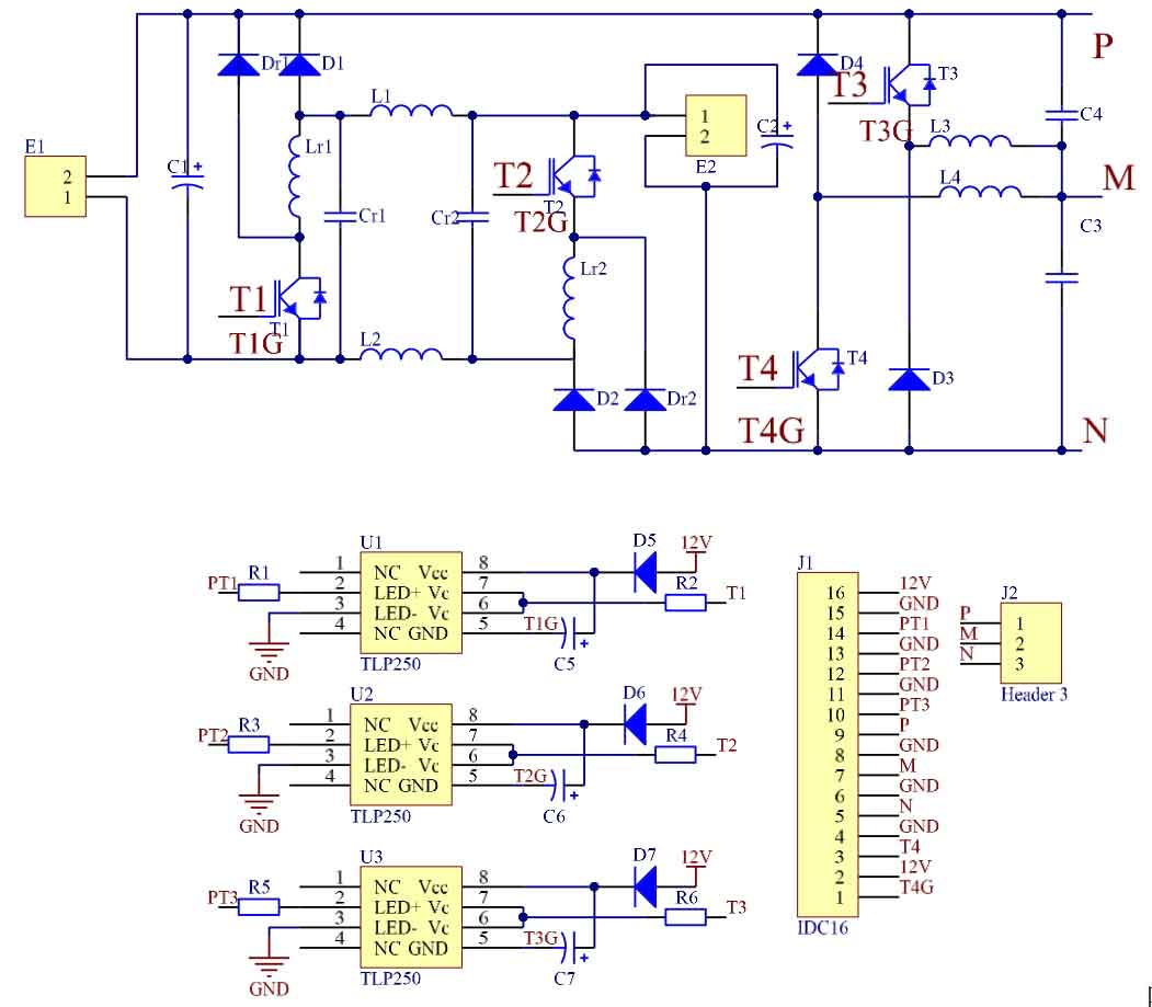
The corresponding IGBT driver chip is selected as TLP250 optocoupler, which mainly consists of a light-emitting diode and a photodetector inside. When the input electrical signal is at a high level, the light-emitting diode couples with the photodetector and outputs a high level on the output side under the action of the power supply. The TLP250 adopts a structure of optical coupling isolation, which effectively reduces noise, improves anti-interference and voltage resistance performance, and has a certain negative voltage turning off ability. Therefore, it is widely used in IGBT driving work scenarios.
For the convenience of debugging, this article designs the front-end voltage regulation circuit and the back-end inverter circuit separately.
The switching frequency of the front-end voltage regulation circuit is higher, while the switching frequency of the back-end inverter circuit is lower, which is also one of the reasons for separating the two designs to achieve better electromagnetic compatibility.
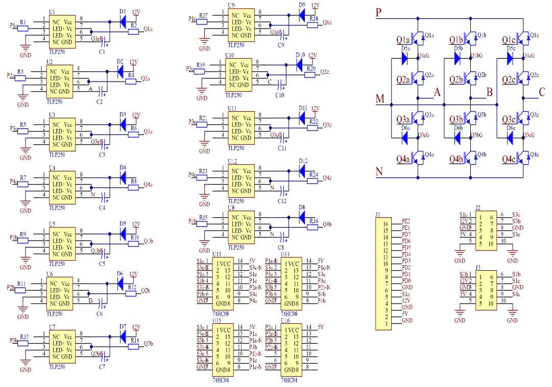
In the later stage inverter circuit, in order to prevent bus short circuits caused by four IGBTs conducting simultaneously in each phase, this paper also uses 74HC08 four input AND gate and 74HC04 four input inverter to add hardware braking function to the driving signals of each phase bridge arm. Taking the A-phase bridge arm as an example, Q1a and Q3a are complementary switching tubes. The switch pulse signal of Q1a and the pulse signal output by Q3a through the inverter are input in parallel to 74HC08. At this time, the output of the AND gate is used as the driving signal of Q1a. Only when Q3a is in the off state can the AND gate output a high level, and Q1a can conduct. This solution can effectively solve the problem of short circuit in the busbar when the dead time setting fails.
4. Summary
This article mainly introduces the hardware implementation scheme of a three-level adjustable two-stage solar inverter. The hardware implementation plan mainly includes the design of the main control circuit, the selection of different voltage and current measurement schemes, and the separate design of the front-end voltage regulation circuit and the back-end inverter circuit. Due to limitations in laboratory conditions, as well as personal and other objective factors, this article has only completed the design work for the hardware circuit.
Through in-depth understanding of photovoltaic power generation and three-level solar inverters, this paper proposes a new two-stage inverter structure to address a series of problems brought by traditional boost two-stage solar inverters. Calculate the LC parameters and build a simulation experimental platform using Simulink. Through simulation verification, the amplitude frequency characteristics of the three-phase output voltage are good, and the overall THD is low, achieving the expected goals, proving the feasibility of this scheme. And a loss model for the overall system was established, and the maximum conversion efficiency reached 98.79% and the weighted inverter efficiency reached 98.47% through calculation. The efficiency index of this structure is better than that of traditional boost two-stage solar inverters. At the same time, a low-power prototype design scheme for a new two-stage inverter structure is provided. The main innovations of this paper’s work are as follows:
(1) A novel three-level adjustable two-stage inverter structure is proposed. The front-end circuit adopts a dual power supply overlapping boost circuit, which greatly reduces the current and switching amplitude of the boost converter compared to a regular boost converter. By using two buck converters to supply power to the midpoint of the later stage, the midpoint voltage can be effectively adjusted.
(2) Based on the novel topology proposed in this article, a mathematical model is established for the voltage of the rear three-phase and the voltage of the front circuit. A strategy for joint control of the front and rear stages is proposed, which makes the bus and midpoint voltage equal to the voltage of the rear three-phase line, greatly reducing the switching losses and filter losses of the rear stage solar inverter.