
The photovoltaic grid connected power generation system consists of three parts: photovoltaic panel components, grid connected solar inverters, and the mains network. Grid connected solar inverters can be divided into DC boost modules and inverter grid connected modules. This chapter mainly studies the solar inverter grid connection module. By analyzing the four working modes of the H6 full bridge solar inverter circuit, the conduction order of the six power switches is determined, and the design method of the output side inductance and capacitance of the solar inverter circuit is introduced.
1. Circuit analysis of grid connected solar inverters
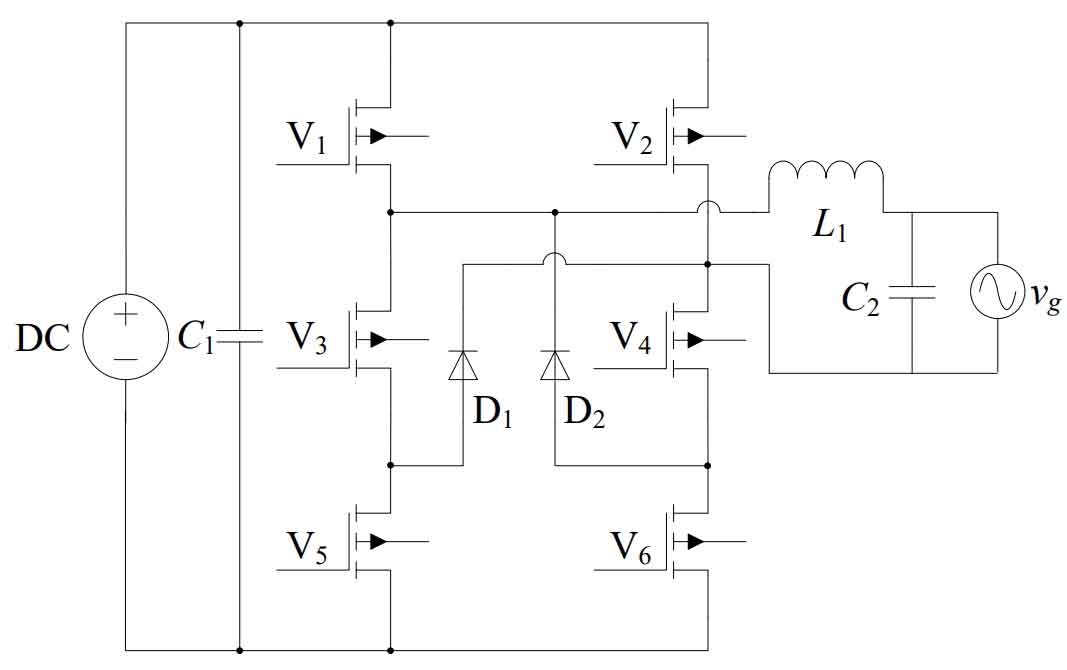
The solar inverter circuit topology used in this paper is an H6 full bridge structure, as shown in Figure 1. In the figure, C1 serves as the stabilizing capacitor at the input end of the solar inverter (to stabilize the DC bus voltage and reduce voltage fluctuations); V1~V6 are power switching devices for full bridge circuits; D1 and D2 are freewheeling diodes; Inductance L1 and capacitor C2 form a low-pass filter (which filters out high-frequency signals from the output waveform of the solar inverter to obtain a 50Hz sine waveform).
By analyzing the positive and negative half axis waveforms of the grid connected current, the working state of the solar inverter can be divided into four situations, corresponding to Figure (a), Figure (b), Figure (c), and Figure (d) in Figure 2. The dashed part in the figure represents the part where the current does not flow.
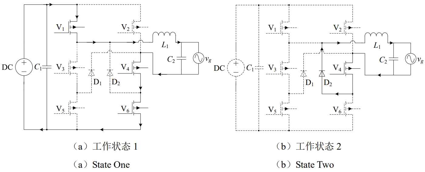

In Figure 2, Figures (a) and (b) represent the schematic diagram of the grid connected current flow direction when the output voltage of the solar inverter operates on the positive half axis. Figure (a) shows working state 1, where the DC terminal voltage is charged to inductor L1 and capacitor C2 through conductive power tubes V1, V4, and V6. It can be observed that the upper end of capacitor C2 is positive and the lower end is negative (output voltage is a positive half axis waveform). The solar inverter transmits power to the grid, and at this time, the grid connected current continues to increase, causing inductor L1 to store more energy.
Figure (b) shows working state 2, where power tubes V1 and V6 are turned off, and the current in the inductor continues to flow through power tubes V4 and D1. The voltage of the C2 capacitor remains positive at the upper end and negative at the lower end (output voltage is a positive half axis waveform). At this time, the solar inverter still feeds the grid, and the energy stored in inductor L1 continuously decreases, leading to a continuous decrease in grid connected current.
Figures (c) and (d) represent the schematic diagram of the grid connected current flow when the output voltage of the solar inverter operates on the negative half axis. Figure (c) shows working state 3, where the DC end charges the inductor L1 and capacitor C2 through conductive power tubes V2, V3, and V5. It is evident that the upper end of capacitor C2 is the negative electrode and the lower end is the positive electrode (with an output voltage of negative half axis waveform). In this working state, the solar inverter transmits power to the mains, and the grid connected current continuously increases during this time, resulting in the energy stored in inductor L1 continuously increasing.
Figure (d) shows working state 4. When the power tubes V2 and V5 are turned off, the current in the inductor continues to flow through the power tubes V3 and D2. The voltage of the C2 capacitor is negative at the upper end and positive at the lower end (the output voltage is a negative half axis waveform). At this time, the solar inverter feeds the mains power, and the energy stored in inductor L1 continuously decreases, leading to a continuous decrease in grid connected current.
Through the above analysis, the working logic of six switching power transistors can be obtained. V1 and V6 control the high-frequency switching transistors that output the positive half axis of the grid connected current, while V2 and V5 represent the high-frequency switching transistors that control the negative half axis of the output grid connected current. At the same time, V4 and V3 are a pair of complementary power frequency switching transistors. Through analysis, the switching timing logic of these power transistors can be obtained, as shown in Figure 3.
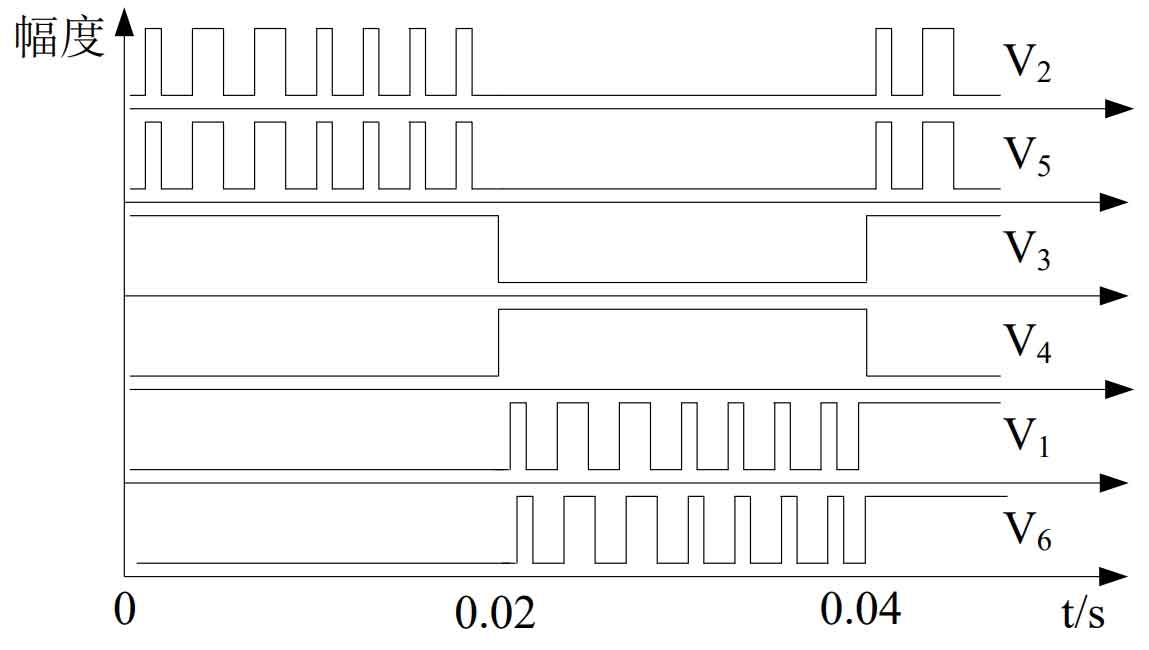
In Figure 3, when V4 is conducting, V1 and V6 switch tubes are controlled at a switching frequency of 20kHz for output, while when V3 is conducting, V2 and V5 switch tubes are also controlled at a switching frequency of 20kHz for output. When V3 is conducting, V4 must be closed. By utilizing the switch logic sequence of V1~V6 in Figure 3, the driving signals of these 6 MOS transistors can be designed.
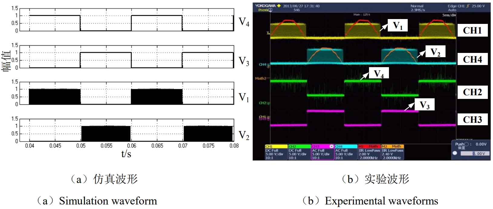
Through MATLAB simulation and actual prototype testing, the correctness of the driving waveforms corresponding to V1~V6 in Figure 3 can be verified. Figure (a) in Figure 4 shows the driving waveform obtained in simulation, Figure (b) shows the actual measured driving waveform, and CH1~CH4 in Figure (b) represent the channel numbers of the oscilloscope.
The grid connected solar inverter controls the power transistors V1~V6 to turn on and off according to the control logic shown in Figure 3, resulting in a series of rectangular waves with different pulse widths. The obtained rectangular waves are passed through the LC low-pass filter (composed of inductor L1 and capacitor C2) at the rear end of the solar inverter to filter out the high-frequency harmonic components and obtain a 50Hz sine waveform.
2. Design of AC side filter
According to the modulation principle of SPWM (Sinusoidal Plus Width Modulation), a grid connected solar inverter outputs a series of rectangular pulses with varying widths, which are filtered by a low-pass filter to obtain a sinusoidal signal. The implementation principle is to expand the rectangular wave U with amplitude U0 into Fourier series:
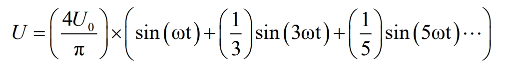
According to the formula, the rectangular wave U is expanded into a series of sine waveforms with different frequencies through Fourier series. These waveforms are filtered out through a low-pass filter with a cutoff frequency greater than 50Hz to filter out sine signals with a frequency of 50Hz. The low-pass filter used in this chapter is composed of inductors and capacitors connected in series. Due to the use of a 20kHz switching frequency in this article, it is necessary to consider filtering out this switching frequency to reduce the interference of this high-frequency signal on the system. In engineering, it is considered infinitesimal if it is less than 0.1 times a certain value, and infinite if it is greater than 10 times a certain number. According to this requirement, it is necessary to set the cutoff frequency of the low-pass filter to satisfy the inequality:
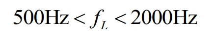
According to the inequality, the cutoff frequency range of this low-pass filter is required to be between 500Hz and 2000Hz. Therefore, in this chapter, 1kHz is selected as the cutoff frequency for the low-pass filter design.
Due to the fact that the design of the filter not only affects the dynamic and static response of the current loop, but also restricts the determination of the output power, system power consumption, and DC side voltage of the grid connected system, the design of the AC side LC filter is very important. The main functions of the AC side filter of grid connected solar inverters are as follows: Firstly, because the inductance has a certain blocking effect on the current, it effectively suppresses the excessive fluctuation of the output current; Secondly, it can filter out the high-frequency interference components generated by the operation of power switching tubes; Thirdly, the output filtering inductance of the grid connected solar inverter is equivalent to a lever connecting the power grid and H6 inverter bridge. Through it, the amplitude and phase of the grid connected current can be controlled, thereby achieving grid connected operation with a power factor of 1; Fourthly, making grid connected solar inverters have certain damping characteristics is beneficial for the design of control systems.
The design of LC low-pass filters can be done separately from capacitor C and inductor L. When the grid connected solar inverter is in grid connected operation, due to the clamping effect of the grid voltage, the filtering capacitor C is equivalent to the load, so the focus of designing LC low-pass filters is on the design of inductance L.
The design of inductor L is based on the magnitude of current ripple and voltage drop on the inductor. The voltage drop range on inductor L is required to be between 3% and 5% of the output voltage, and the output current ripple should be between 10% and 20% of the output current size (the current ripple should not be too large to prevent it from triggering overcurrent protection). According to the above requirements, the formula can be obtained:
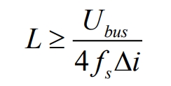
In the formula, Ubus=380V is the DC side bus voltage= 20kHz sf is the frequency of the switching tube; Δ I represents the magnitude of the current ripple (10% to 20% of the effective value of the rated output current, taken as 2A).
Through the formula, it can be obtained that L ≥ 2.375mH.
In general, the reactive power of a capacitor is required to be limited to 15% of the system power. The calculation formula for the size of capacitor C is:
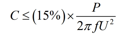
In the formula, f=50Hz is the frequency of the fundamental power supply; P=2000W is the output power; U=311V is the peak output voltage of the solar inverter.
According to the formula: C ≤ 9.88 μ F.
The output filtering inductance and filtering capacitor of the solar inverter in this article are provided by Sanda Technology Co., Ltd. The given parameters are as follows: inductance parameter L=2.5mH, capacitance parameter C=4.7 μ F. The given parameters meet the requirements of theoretical analysis and also meet the requirements of the formula.
3. Summary
A detailed analysis was conducted on the working mode of the H6 full bridge solar inverter circuit, and the working sequence of six switching power transistors was determined, which will help to better design the driving control program of power switching transistors. At the same time, according to the design requirements of the AC side filter, the range of inductance and capacitance values was theoretically calculated, and the rationality of the inductance and capacitance values was verified by comparing the inductance and capacitance parameters provided by the company.