
I started this work from a simple but pressing engineering question: how can a small solar module deliver clean, stable, grid-compatible alternating current with high efficiency, low harmonic distortion, and reliable maximum power tracking when sunlight and temperature are constantly changing? My research and design work therefore focused on a grid-connected micro-inverter rated at about 200 W. I treated the system as a complete power conversion chain, beginning with the photovoltaic module, moving through maximum power point tracking, then through a high-frequency push-pull step-up stage, a full-bridge inverter, an output filter, and finally a grid-connected current control strategy. Throughout this work, I kept returning to the same central idea: solar inverters are not merely direct current to alternating current converters; they are the interface between an intermittent renewable source and a stiff, sometimes distorted, and frequently disturbed utility grid.
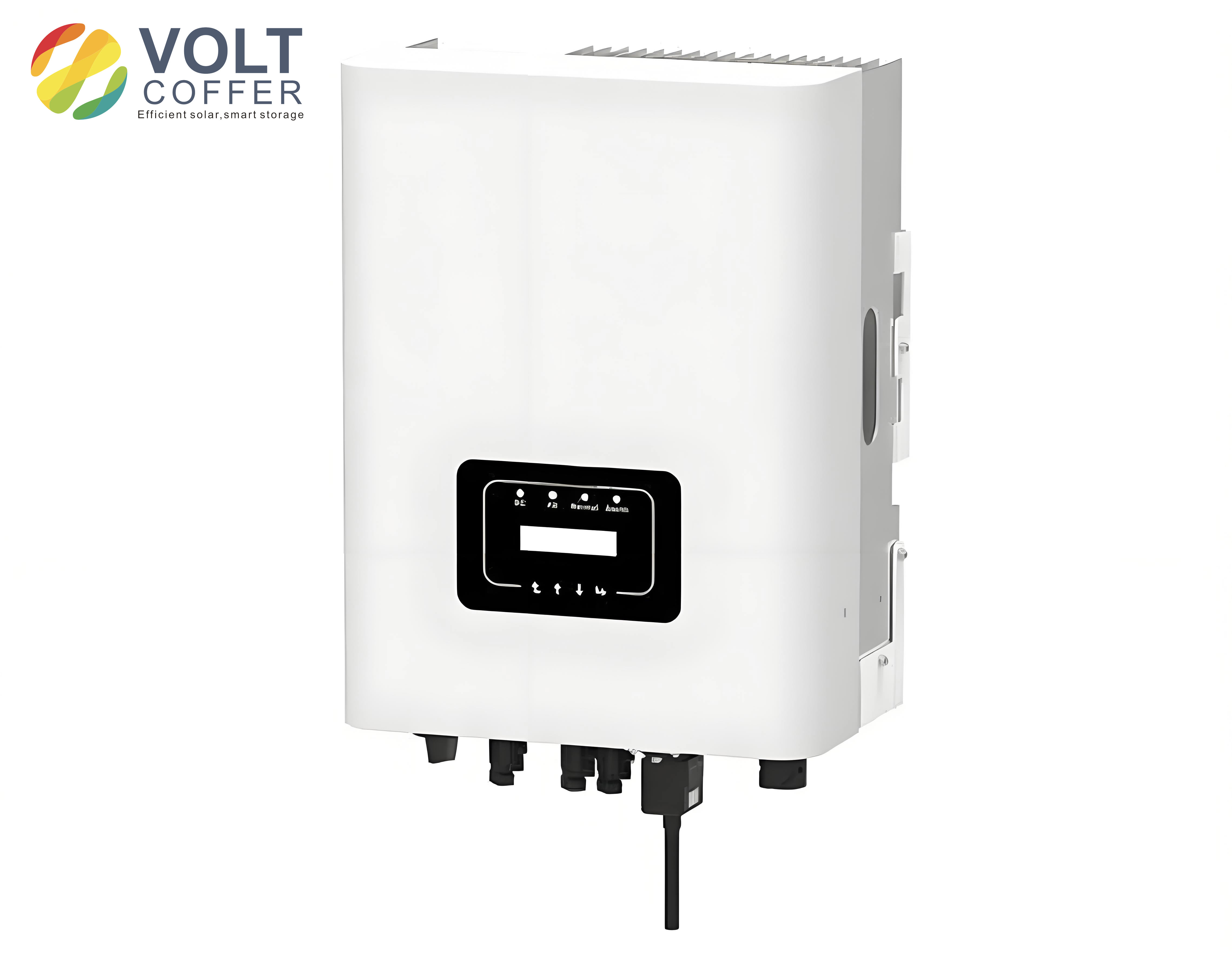
My design objective was not only to build a functioning laboratory prototype, but also to develop a clear analytical path that explains why each major choice was made. I wanted the resulting micro-inverter to accept a low direct-current input, produce a regulated sinusoidal output, operate at a switching frequency high enough to reduce magnetic component size, and maintain output quality under varying load conditions. I also wanted to study grid connection methods carefully, because a micro-inverter that performs well on a resistive test load may still behave poorly when connected to the grid. The final design target that I used to guide the work is summarized in the following table.
| Parameter | Design target | Remarks |
|---|---|---|
| Input nominal direct-current voltage | 24 V | Low-voltage photovoltaic module or laboratory direct-current source |
| Output alternating-current voltage | 220 V RMS, plus or minus 5 percent | Single-phase utility-compatible level |
| Output frequency | 50 Hz, plus or minus 5 percent | Grid synchronization requirement |
| Rated output power | 200 W | Micro-inverter power class |
| Total harmonic distortion | Below 5 percent | Target for output current and voltage quality |
| Conversion efficiency | At least 85 percent | Measured from direct-current input to alternating-current output |
I organized the study into several tightly connected parts. First, I analyzed the photovoltaic source and its maximum power point behavior. Second, I selected and examined the inverter topology. Third, I studied sinusoidal pulse-width modulation, harmonic generation, and filtering. Fourth, I compared grid-connected current control strategies. Fifth, I implemented the hardware and software and evaluated the experimental results. I found that the most important lesson is that solar inverters must be designed as systems, not as isolated converter stages. A small error in maximum power tracking, a poorly chosen dead time, or an inadequate output filter can degrade the entire system even if each individual stage appears acceptable.
Photovoltaic Source and Maximum Power Point Behavior
I began with the photovoltaic cell because the behavior of solar inverters is ultimately constrained by the source. A photovoltaic cell is essentially a large-area semiconductor diode that generates current when illuminated. The photogenerated current is separated by the built-in electric field of the junction, producing a voltage across the terminals. When a load is connected, current flows. The single-diode equivalent circuit that I used for analysis contains a current source, a diode, a series resistance, and a shunt resistance. The current-voltage relationship can be written as shown below.
$$ I = I_L – I_D \left( e^{\frac{q(V + I R_s)}{n K T}} – 1 \right) – \frac{V + I R_s}{R_{sh}} $$
In this expression, I represents the terminal current, I_L is the photogenerated current, I_D is the diode saturation current, q is the elementary charge, V is the terminal voltage, R_s is the series resistance, n is the diode ideality factor, K is Boltzmann’s constant, T is the absolute temperature, and R_{sh} is the shunt resistance. I used this model because it captures the most important physical effects while remaining practical for simulation. The series resistance reduces the fill factor and therefore lowers the achievable output power. The shunt resistance represents leakage paths and becomes especially important under low irradiance.
After building the model, I examined how temperature and irradiance affect the current-voltage and power-voltage curves. I found that increasing irradiance raises the short-circuit current strongly and also increases the maximum available power. Increasing temperature, on the other hand, reduces the open-circuit voltage and slightly increases the short-circuit current, but the net effect is usually a reduction in maximum power. This behavior is critical for solar inverters because the operating point that yields maximum power moves as environmental conditions change. A fixed operating voltage cannot remain optimal throughout the day.
| Condition | Effect on short-circuit current | Effect on open-circuit voltage | Effect on maximum power |
|---|---|---|---|
| Irradiance increases | Increases nearly proportionally | Increases slightly | Increases significantly |
| Temperature increases | Increases slightly | Decreases noticeably | Usually decreases |
| Series resistance increases | Little change at short circuit | Slight reduction | Reduces fill factor and power |
| Shunt resistance decreases | Little change at high irradiance | Reduction at low irradiance | Reduces power at low irradiance |
I then moved to maximum power point tracking, often abbreviated as MPPT. The maximum power point is the point on the power-voltage curve where the derivative of power with respect to voltage is zero. Mathematically, I wrote this condition as follows.
$$ \frac{dP}{dV} = \frac{d(VI)}{dV} = I + V \frac{dI}{dV} = 0 $$
Dividing by V gives the condition that I used repeatedly in my control algorithm.
$$ \frac{I}{V} + \frac{dI}{dV} = 0 $$
The first term is the instantaneous conductance, and the second term is the incremental conductance. When their sum is zero, the photovoltaic source is at the maximum power point. When the sum is positive, the operating voltage is below the maximum power point and should be increased. When the sum is negative, the operating voltage is above the maximum power point and should be decreased. This is the basis of the incremental conductance method.
I compared several maximum power point tracking methods before choosing the one that I would improve. The constant-voltage method is simple but inaccurate because it ignores temperature and irradiance. The perturb-and-observe method is widely used and relatively simple, but it often oscillates around the maximum power point when a fixed perturbation step is used. The conventional incremental conductance method improves the tracking direction, but if the voltage step is fixed, it still faces a trade-off between tracking speed and steady-state accuracy. I summarized these trade-offs in the table below.
| Method | Main idea | Advantages | Limitations |
|---|---|---|---|
| Constant-voltage method | Hold the operating voltage near a predetermined value | Simple and low cost | Poor accuracy under changing temperature and irradiance |
| Perturb-and-observe | Perturb the voltage and observe power change | Simple and widely used | Fixed step causes oscillation and slow tracking |
| Conventional incremental conductance | Compare instantaneous and incremental conductance | Better direction detection than perturb-and-observe | Fixed voltage step still limits speed and accuracy |
| Variable-step incremental conductance | Adjust step size according to distance from maximum power point | Fast away from maximum and accurate near maximum | Requires more computation and careful limits |
Because I wanted better performance without excessive complexity, I proposed and studied a variable-step incremental conductance method. The central idea is that the magnitude of the conductance mismatch indicates how far the operating point is from the maximum power point. Far from the maximum, the step can be large. Close to the maximum, the step should be small to avoid oscillation. I also introduced a maximum step limit to protect the system when irradiance or temperature changes abruptly and the measured derivative becomes very large. The logic can be summarized as follows.
$$ \Delta V_{ref} = \begin{cases} \Delta V_{max}, \text{ if the magnitude of } \frac{I}{V} + \frac{dI}{dV} \text{ is large} \\ \frac{I}{V} + \frac{dI}{dV}, \text{ if the magnitude of } \frac{I}{V} + \frac{dI}{dV} \text{ is small} \end{cases} $$
In implementation, I computed the voltage and current differences between successive samples, calculated the conductance terms, and updated the reference voltage only after checking for zero voltage change and for numerical noise. I found that this method tracked the maximum power point more smoothly than a fixed-step method. It reached the vicinity of the maximum quickly when the operating point was far away, and it reduced the step near the maximum so that the power did not oscillate as strongly. This was one of the most useful outcomes of my study because it directly affects the energy yield of solar inverters.
I also considered the practical issue of sampling noise. In a real solar inverter, current and voltage measurements contain switching ripple and electromagnetic interference. A derivative-based method can become unstable if the measurements are noisy. Therefore, I used filtering and a minimum step threshold. If the conductance mismatch was smaller than a chosen threshold, I held the reference voltage constant rather than making a tiny correction. This prevented the controller from chasing noise. The result was a maximum power point tracker that behaved well in simulation and remained practical for a digital signal processor implementation.
Inverter Topology and Power Stage Selection
After studying the source, I turned to the power conversion topology. A micro-inverter must usually perform two functions: step up the low direct-current voltage from the photovoltaic module and invert the resulting higher direct-current voltage into alternating current. Because the input voltage is low, usually 24 V or 48 V in this power class, the input current is relatively high. For a 200 W system at 24 V, the input current is approximately 8.3 A at full power, and with losses it can be higher. This means that conduction losses and transformer utilization are important. I compared several possible topologies before selecting the one that I would build.
| Topology | Structure | Advantages | Disadvantages |
|---|---|---|---|
| Non-isolated boost plus full bridge | Boost step-up followed by direct-current to alternating-current bridge | Simple, fewer magnetic components, high efficiency potential | No galvanic isolation, safety and grounding issues |
| Half-bridge inverter | Two switches and split direct-current bus | Fewer switches, simple drive | Higher current stress, lower voltage utilization |
| Full-bridge inverter | Four switches forming two legs | Good voltage utilization, suitable for higher power | More switches and more complex drive |
| Push-pull plus full bridge | Push-pull step-up transformer followed by full-bridge inverter | Isolation, voltage step-up, good switch utilization | Transformer design and leakage inductance must be controlled |
| Flyback plus unfolding bridge | Flyback conversion with polarity unfolding | Simple and low cost at low power | High peak current, limited power, higher losses |
I selected a high-frequency push-pull step-up stage followed by a full-bridge inverter. In my design, the photovoltaic direct-current input is first filtered by an input capacitor. Two switching devices drive the primary side of a high-frequency transformer in a push-pull manner. The transformer provides voltage step-up and galvanic isolation. The secondary side is rectified and filtered to form a high-voltage direct-current bus. This bus is then inverted by a full-bridge circuit into a sinusoidal pulse-width modulated waveform. Finally, the output filter removes switching harmonics and produces a sinusoidal voltage suitable for the load or for grid connection.
The push-pull stage has several advantages for this application. It uses two switches referenced to the same ground, which simplifies the gate drive compared with a half-bridge or full-bridge primary. The transformer primary is driven in both directions, so the magnetic core can be used efficiently. The turns ratio can be chosen to raise the low input voltage to a level high enough for a 220 V alternating-current output. I used a high switching frequency for the push-pull stage to reduce the size of the transformer. However, I also had to pay attention to flux imbalance, leakage inductance, and dead time. If the two push-pull switches conduct at the same time, the transformer primary can be shorted, which can damage the switches. Therefore, I set the pulse-width modulation duty cycle below 50 percent and included dead time.
For the full-bridge inverter, I chose four power switches arranged in two legs. The full-bridge topology allows the direct-current bus voltage to be applied to the load in either polarity, which is necessary for sinusoidal output. It also distributes current among switches and provides good utilization of the direct-current bus. I used sinusoidal pulse-width modulation to control the four switches. The output of the bridge is a train of pulses whose widths vary sinusoidally. The filter then extracts the fundamental component and attenuates the switching harmonics.
The semiconductor devices were selected with voltage and current margins. In the low-voltage push-pull stage, the switch voltage rating must exceed the reflected transformer voltage plus leakage spike. The current rating must exceed the input current with margin. In the high-voltage full-bridge stage, the switches must block the direct-current bus voltage plus transients. I also considered gate drive requirements. A gate driver must provide enough peak current to charge and discharge the gate capacitance quickly, otherwise switching losses increase. Negative turn-off voltage can be helpful for reliable turn-off of some devices. I summarized the main power-stage choices in the table below.
| Stage | Function | Key design consideration | Selected approach |
|---|---|---|---|
| Input filter | Reduce source current ripple | Capacitor ripple current and voltage rating | Low equivalent series resistance capacitor near the input |
| Push-pull step-up | Raise 24 V direct current to a high-voltage bus | Transformer turns ratio, flux balance, dead time | High-frequency transformer with two ground-referenced switches |
| Secondary rectifier | Convert transformer secondary alternating current to direct current | Reverse recovery and conduction loss | Fast rectifiers with snubbing where needed |
| Bus capacitor | Support the high-voltage direct-current link | Ripple current, equivalent series resistance, voltage rating | Electrolytic capacitor with low equivalent series resistance |
| Full-bridge inverter | Generate sinusoidal pulse-width modulated voltage | Dead time, switching loss, voltage rating | Four-switch bridge with isolated or high-side drives |
| Output filter | Attenuate switching harmonics | Cutoff frequency, load variation, total harmonic distortion | Two-stage LC filter |
Sinusoidal Pulse-Width Modulation and Harmonic Analysis
I spent considerable effort on sinusoidal pulse-width modulation because it determines the harmonic content of solar inverters. The basic principle is to compare a sinusoidal reference wave with a triangular carrier. When the reference is higher than the carrier, the bridge applies one polarity; when it is lower, the bridge applies the opposite polarity or zero, depending on the modulation scheme. The resulting pulse widths vary sinusoidally, so the fundamental component of the output follows the reference. I studied both analog and digital generation methods and chose a digital approach because it is flexible, repeatable, and easy to integrate with maximum power point tracking and protection functions.
For digital generation, I analyzed natural sampling, symmetric regular sampling, and asymmetric regular sampling. Natural sampling defines the switch transition at the exact intersection of the sinusoidal reference and the triangular carrier. It gives the best harmonic performance in theory, but the switching instants are solutions of transcendental equations, which makes real-time computation difficult. Symmetric regular sampling updates the duty cycle once per carrier cycle, usually at the carrier peak or valley. It is simple and computationally efficient. Asymmetric regular sampling updates twice per carrier cycle, at both peak and valley, which improves accuracy at the cost of more computation. I compared these methods as shown below.
| Sampling method | Update instants | Computational burden | Harmonic performance | Implementation suitability |
|---|---|---|---|---|
| Natural sampling | Exact intersections | Very high | Best theoretical | Not practical for simple digital control |
| Symmetric regular sampling | Once per carrier cycle | Low | Good | Very suitable for digital signal processors |
| Asymmetric regular sampling | Twice per carrier cycle | Moderate | Better than symmetric | Suitable when computation is available |
For symmetric regular sampling, I used the following duty-cycle relationship. The on-time of the switch in one carrier period can be expressed in terms of the modulation index and the sampled sine value.
$$ t_{on} = \frac{T_s}{2} \left( 1 + M \sin(\omega_r t_1) \right) $$
Here, T_s is the carrier period, M is the modulation index, \omega_r is the angular frequency of the sinusoidal reference, and t_1 is the sampling instant. The modulation index and carrier ratio are defined as follows.
$$ M = \frac{U_{sm}}{U_r} $$
$$ N = \frac{f_r}{f_s} $$
In these equations, U_{sm} is the amplitude of the sinusoidal reference, U_r is the amplitude of the triangular carrier, f_r is the reference frequency, and f_s is the carrier frequency. I chose a carrier frequency much higher than the reference frequency so that the switching harmonics appear at high frequency and can be filtered effectively. For a 50 Hz output, a carrier frequency of several tens of kilohertz is typical. In my design, I used a carrier frequency of about 30 kHz for the full-bridge stage and about 50 kHz for the push-pull stage.
I then studied modulation schemes. Bipolar modulation applies positive and negative bus voltage alternately during each carrier cycle. Unipolar modulation applies either zero and positive voltage or zero and negative voltage, depending on the half-cycle of the reference. Double-frequency modulation, also called unipolar double-frequency modulation, drives one leg with a comparison between the reference and the carrier and drives the other leg with a comparison between the reference and an inverted carrier or an inverted reference and the same carrier. This effectively doubles the output pulse frequency, which pushes the dominant harmonics to higher frequencies and makes filtering easier. I found that double-frequency sinusoidal pulse-width modulation gave better harmonic performance for the same filter, so I used it in the full-bridge stage.
To design the filter, I needed to understand the harmonic spectrum. I analyzed the Fourier series of the bridge output voltage. For a half-bridge leg with bipolar modulation, the output voltage can be expressed as a sum of a direct-current term, the fundamental component, and harmonics at multiples of the carrier frequency. The harmonic angular frequencies are given by combinations of the carrier and reference frequencies.
$$ \omega_h = n \omega_c \pm k \omega_r $$
For double-frequency modulation of a full bridge, the harmonic amplitudes can be described using Bessel functions. A representative expression for the harmonic amplitude is shown below.
$$ A_h = \frac{4 U_d}{n \pi} J_k \left( \frac{n \pi M}{2} \right) $$
In this expression, U_d is the direct-current bus voltage, n is the carrier harmonic index, k is the sideband index, M is the modulation index, and J_k is the Bessel function of the first kind of order k. I used this analysis to confirm that the dominant harmonics for double-frequency modulation appear at higher frequencies than for simple bipolar modulation. This is important for solar inverters because a smaller and more effective filter can be used when the switching harmonics are farther from the fundamental.
After modulation, the bridge output is a pulse train containing the desired fundamental and many high-frequency components. The filter must pass the fundamental with little attenuation while strongly attenuating the switching harmonics. A simple LC filter can do this, but I found that its output quality changed noticeably when the load changed. Under light load, the filter damping is low and the output can peak or ring near resonance. Under heavy load, the cutoff behavior changes. To improve the load adaptability, I proposed a two-stage LC-LC series filter. The first stage primarily attenuates the bridge switching harmonics, and the second stage further smooths the voltage across the load. The topology is simple, but the transfer function is fourth order, so I analyzed it carefully.
The transfer function of the LC-LC filter can be written as follows.
$$ H(s) = \frac{U_o(s)}{U_i(s)} = \frac{1}{a s^4 + b s^3 + c s^2 + d s + 1} $$
The coefficients are determined by the inductances, capacitances, and load resistance.
$$ a = L_1 L_2 C_1 C_2 $$
$$ b = \frac{L_1 L_2 C_1}{R} $$
$$ c = L_1 C_1 + L_2 C_2 + L_2 C_1 $$
$$ d = \frac{L_1 + L_2}{R} $$
In these equations, L_1 and L_2 are the filter inductors, C_1 and C_2 are the filter capacitors, and R is the load resistance. I chose the component values so that the first resonant frequency is well below the switching frequency but well above the fundamental frequency. The cutoff frequency of an LC section is approximately as follows.
$$ f_c = \frac{1}{2 \pi \sqrt{L C}} $$
I selected the inductors based on the maximum allowable current ripple. For a full-bridge inverter, the inductor current ripple depends on the bus voltage, the output voltage, the switching frequency, and the inductance. A common design guideline is to keep the ripple current between about 15 percent and 25 percent of the rated peak current. This keeps core loss and conduction loss within reasonable limits while allowing a physically small inductor. I also selected capacitors with low equivalent series resistance because high equivalent series resistance increases ripple voltage and losses.
| Filter parameter | Selected value | Design reason |
|---|---|---|
| First inductor L_1 | Approximately 1.68 mH | Limits bridge current ripple and sets first cutoff |
| Second inductor L_2 | Approximately 16.8 mH | Provides additional attenuation of switching harmonics |
| First capacitor C_1 | Approximately 1.4 microfarad | Forms first LC stage with L_1 |
| Second capacitor C_2 | Approximately 1.68 microfarad | Forms second LC stage with L_2 and improves load immunity |
| Cutoff target | About 3 kHz | Below switching frequency and above fundamental by a wide margin |
I simulated the filter with different load resistances. With a light load of about 200 ohms, the output waveform was smooth and stable. With a heavy load of about 10 ohms, the output remained stable and the harmonic distortion stayed low. The total harmonic distortion in the simulation was about 0.96 percent, which is much lower than the design target of 5 percent. This confirmed that the two-stage LC filter was a worthwhile improvement over a single LC stage for solar inverters that must operate under variable load conditions.
Grid-Connected Current Control Strategies
Once the power stage and filter were understood, I studied how to connect the micro-inverter to the grid. A grid-connected solar inverter usually operates as a current source rather than a voltage source. The utility grid is a stiff voltage source with its own fluctuations, so forcing a voltage onto the grid can cause large currents and instability. Instead, the inverter controls its output current to be sinusoidal and in phase with the grid voltage. This is the standard approach for grid-tied solar inverters. I analyzed three common current control strategies: hysteresis current control, proportional-integral control, and deadbeat control.
Hysteresis current control compares the measured grid current with a reference current. The error is fed into a comparator with a hysteresis band. When the error exceeds the upper band, the inverter switches to increase the current. When the error falls below the lower band, the inverter switches to decrease the current. The switching frequency is not fixed; it depends on the inductance, the direct-current bus voltage, and the grid voltage. This method is simple, robust, and has good dynamic response. However, the variable switching frequency makes filter design difficult and can produce a broad harmonic spectrum. It also causes higher switching losses when the hysteresis band is narrow.
| Control method | Principle | Advantages | Disadvantages |
|---|---|---|---|
| Hysteresis current control | Switch according to current error band | Simple, fast, robust | Variable switching frequency, broad harmonic spectrum |
| Proportional-integral control | Regulate current error with proportional and integral gains | Fixed switching frequency, good steady-state accuracy | Requires tuning, can be affected by grid voltage |
| Deadbeat control | Calculate duty cycle from discrete system model | Fast response, high waveform quality | Depends on accurate model, sensitive to parameter mismatch |
Proportional-integral control is widely used in industrial systems, and I found it suitable for grid-connected solar inverters when combined with a feedforward term. The current error is processed by a proportional-integral controller to produce a modulation command. The command is compared with a triangular carrier to generate the gate signals. The proportional term improves the transient response, while the integral term eliminates steady-state error. The transfer function of the proportional-integral controller is shown below.
$$ G_3(s) = k_p + \frac{k_i}{s} $$
In this expression, k_p is the proportional gain and k_i is the integral gain. I modeled the inverter as a gain, the filter as a first-order or higher-order transfer function, and the grid as a disturbance. The closed-loop current can be expressed as a combination of the reference current and the grid voltage disturbance.
$$ I_L(s) = \frac{G_1(s) G_2(s) G_3(s)}{1 + G_1(s) G_2(s) G_3(s)} I_{ref}(s) – \frac{G_1(s) G_4(s)}{1 + G_1(s) G_2(s) G_3(s)} U_{ac}(s) $$
Here, G_1(s) represents the filter, G_2(s) represents the inverter gain, G_3(s) is the current controller, and G_4(s) represents the grid voltage feedforward path. To cancel the effect of the grid voltage on the current, the feedforward path should satisfy the following relationship.
$$ G_4(s) = \frac{1}{G_2(s)} $$
If the inverter gain is approximately a constant k_{spwm}, then the feedforward path becomes as follows.
$$ G_4(s) = \frac{1}{k_{spwm}} $$
I found that adding grid voltage feedforward significantly reduced the influence of grid voltage distortion on the output current. This is important because the grid voltage is not a pure sine wave in practice. Harmonics and voltage sags can distort the current if the controller does not compensate for them. With feedforward and well-tuned proportional-integral gains, the output current remained sinusoidal and in phase with the grid voltage in simulation.
Deadbeat control is another attractive method for grid-connected solar inverters because it can achieve very fast response. It uses a discrete model of the inverter and filter to calculate the duty cycle that will force the current to reach the reference value in the next sampling period. For a filter inductor L, equivalent resistance R, grid voltage U_{ac}, and direct-current bus voltage U_{dc}, the discrete equation can be written as follows.
$$ U_n(k) = \frac{L}{T_s} \left( i_L(k+1) – i_L(k) \right) + R i_L(k) + U_{ac}(k) $$
Solving for the duty cycle gives the following expression.
$$ D(k) = \frac{ \frac{L}{T_s} \left( i_{ref}(k+1) – i_L(k) \right) + R i_L(k) + U_{ac}(k) }{ U_{dc} } $$
In this equation, T_s is the sampling period, i_L(k) is the measured current, i_{ref}(k+1) is the reference current for the next sample, and U_{ac}(k) is the measured grid voltage. The duty cycle is applied directly to the pulse-width modulator. Deadbeat control has no need for a triangular carrier in the same way as proportional-integral control, so the output current can have low harmonic content if the model is accurate. However, it is sensitive to parameter errors, measurement noise, and delays. In my simulation, deadbeat control produced excellent waveform quality under ideal conditions, but its performance degraded when the inductance or grid voltage was not exactly known. For a low-cost micro-inverter, this sensitivity is a practical concern.
I compared the three methods and decided to use proportional-integral control with grid voltage feedforward for the experimental grid-connection study. The main reason is that it offers a good balance between performance, robustness, and implementation simplicity. Hysteresis control is simple but has variable switching frequency, which complicates output filter design. Deadbeat control is fast but depends on an accurate model. Proportional-integral control with feedforward can operate at a fixed switching frequency, works well with the LC-LC filter, and can be implemented in a digital signal processor with reasonable computational load. This choice also aligns with the requirements of practical solar inverters, where reliability and predictable harmonic behavior are often more important than the absolute fastest transient response.
Digital Control Implementation
I implemented the control system on a digital signal processor. I chose a floating-point device because the maximum power point tracking algorithm, the sinusoidal pulse-width modulation calculations, and the proportional-integral control loops benefit from fast arithmetic and high precision. The processor includes multiple enhanced pulse-width modulation modules. Each module contains a time-base counter, counter-compare registers, action qualifiers, dead-band generation, chopper control, event trigger logic, and trip-zone protection. I used these modules to generate the push-pull pulse-width modulation and the full-bridge sinusoidal pulse-width modulation.
The time-base module sets the switching frequency by dividing the system clock and loading a period register. The counter-compare module determines the duty cycle by comparing the counter value with one or more compare registers. The action qualifier decides whether the output pin is set, cleared, or toggled when a compare event occurs. The dead-band module inserts a delay between the turn-off of one switch and the turn-on of another. This is essential for the full bridge to prevent shoot-through. I set the dead time carefully. If the dead time is too long, the output waveform is distorted and the total harmonic distortion increases. If the dead time is too short, the switches may conduct simultaneously and damage the bridge. I also used the trip-zone module for over-current and over-voltage protection. When a fault is detected, the pulse-width modulation outputs are forced to a safe state.
The software flow begins with system initialization. The clock, input-output pins, analog-to-digital converters, timers, and pulse-width modulation modules are configured. Then a sine table is calculated for the sinusoidal pulse-width modulation. The sine table stores the reference values for each carrier period. In the main loop, the controller samples the photovoltaic voltage and current, runs the maximum power point tracking algorithm, updates the reference voltage, and calculates the modulation index. In the pulse-width modulation interrupt, the controller updates the compare registers with the next duty-cycle values. It also samples the grid voltage and current for the current control loop. The interrupt service routine clears the interrupt flag, performs the proportional-integral calculation, applies the feedforward term, and writes the new duty cycle. This structure keeps the control loop synchronized with the switching frequency.
| Software module | Main function | Key registers or variables | Protection or control role |
|---|---|---|---|
| System initialization | Configure clocks, pins, and peripherals | Clock divider, input-output multiplexers | Ensures deterministic startup |
| Pulse-width modulation setup | Set carrier frequency, counting mode, and polarity | Time-base period, compare registers | Defines switching behavior |
| Dead-band setup | Insert delay between complementary switches | Rising-edge and falling-edge delay | Prevents shoot-through |
| Sine table generation | Precompute sinusoidal reference values | Table pointer and modulation index | Produces low-distortion reference |
| Maximum power tracking | Update photovoltaic operating voltage | Voltage and current samples | Maximizes energy harvest |
| Current control interrupt | Regulate grid current | Proportional and integral gains | Maintains sinusoidal current |
| Trip-zone protection | Disable outputs during faults | Trip flags and comparator inputs | Protects hardware |
I paid special attention to analog-to-digital sampling. The photovoltaic voltage and current must be sampled at the same instant to calculate power accurately. The grid voltage and current must also be sampled with attention to phase. I used sample-and-hold circuits and triggered the analog-to-digital converter from the pulse-width modulation module so that the sampling occurred at a fixed point in the switching cycle. This reduced the influence of switching noise. I also averaged multiple samples when high accuracy was needed, although averaging reduces bandwidth and must be balanced against control loop speed.
Experimental Results and Discussion
After completing the design, I built a laboratory prototype and tested it with a 24 V direct-current source. I used an oscilloscope to observe the gate signals, the sinusoidal pulse-width modulation waveform, the filtered output voltage, and the output current. The first test was the push-pull stage. The two gate signals were complementary with dead time, and the transformer secondary produced a high-voltage direct-current bus. I adjusted the duty cycle and the transformer turns ratio so that the bus voltage was sufficient for a 220 V alternating-current output. I confirmed that the dead time prevented simultaneous conduction and that the snubber circuits limited leakage inductance spikes.
The second test was the full-bridge inverter. I used double-frequency sinusoidal pulse-width modulation with a 30 kHz carrier and a 50 Hz reference. The bridge output was a pulse train with sinusoidal width variation. The LC-LC filter produced a clean sinusoidal voltage. When I changed the load, the output remained stable. The measured total harmonic distortion was about 0.96 percent in the simulation and remained below the design target in the experimental test. The output frequency was 50 Hz, and the effective value of the output voltage was approximately 220 V. The output power reached about 200 W.
I also measured efficiency. The conversion efficiency depends on the losses in the switches, the transformer, the rectifiers, the filter inductors, and the control circuits. At rated power, the measured efficiency was about 85 percent. This met the design target, but it also showed that there is room for improvement. The push-pull transformer contributed significant loss, especially copper loss and core loss. The full-bridge switches had both conduction and switching losses. The output filter inductors had copper loss and core loss. Improving the magnetic design, reducing the leakage inductance, selecting lower-loss switches, and optimizing the dead time could raise efficiency further.
| Measured quantity | Result | Design target | Comment |
|---|---|---|---|
| Input direct-current voltage | 24 V | 24 V nominal | Laboratory source used for controlled testing |
| Output alternating-current voltage | About 220 V RMS | 220 V RMS plus or minus 5 percent | Within tolerance |
| Output frequency | 50 Hz | 50 Hz plus or minus 5 percent | Within tolerance |
| Output power | About 200 W | 200 W | Rated power achieved |
| Total harmonic distortion | About 0.96 percent in simulation | Below 5 percent | Two-stage LC filter performed well |
| Conversion efficiency | About 85 percent | At least 85 percent | Met target, with room for improvement |
The experimental results confirmed several of my theoretical conclusions. First, the variable-step incremental conductance method tracked the maximum power point more smoothly than a fixed-step method. It avoided large oscillations and responded well to step changes in irradiance in the simulation. Second, double-frequency sinusoidal pulse-width modulation pushed the dominant harmonics to higher frequencies, which made the output filter more effective. Third, the LC-LC series filter reduced the sensitivity of the output waveform to load changes. Fourth, proportional-integral control with grid voltage feedforward provided stable current regulation and good harmonic performance in simulation. These findings are directly relevant to the design of practical solar inverters.
I also observed several practical problems that are worth discussing. One issue was electromagnetic interference. The high-frequency switching of the push-pull and full-bridge stages generated noise that coupled into the analog sensing circuits. I reduced this by using twisted pairs, short gate loops, ground planes, and RC snubbers. Another issue was thermal management. The switches and transformer heated up during prolonged operation. I used heat sinks and ensured adequate airflow. A third issue was dead-time distortion. Even a small dead time can create low-order harmonics in the output voltage. I minimized dead time while maintaining safe operation and used feedback control to reduce its effect. These practical details are important because solar inverters must operate reliably for many years in outdoor environments.
Comparative Insights and Design Trade-Offs
My study showed that the design of solar inverters involves many trade-offs. Increasing the switching frequency reduces the size of the transformer and filter, but it increases switching losses and electromagnetic interference. Increasing the filter inductance reduces current ripple and harmonic distortion, but it increases cost, size, and copper loss. Increasing the maximum power point tracking speed improves energy harvest under changing conditions, but it can cause instability if the measurements are noisy. Increasing the dead time improves safety, but it distorts the output waveform. These trade-offs must be balanced according to the target application. For a 200 W micro-inverter, size, cost, efficiency, and output quality are all important, so the design must be optimized rather than pushed to an extreme in any single direction.
| Design variable | Increase effect | Decrease effect | Preferred strategy |
|---|---|---|---|
| Switching frequency | Smaller magnetics, higher switching loss and noise | Larger magnetics, lower switching loss | Use the lowest frequency that meets size and harmonic targets |
| Filter inductance | Lower ripple, larger and more lossy | Smaller and cheaper, higher ripple | Limit ripple to a reasonable percentage of rated current |
| Filter capacitance | Lower voltage ripple, larger reactive current | Smaller and cheaper, higher ripple | Choose cutoff well above fundamental and below switching |
| Maximum power tracking step | Faster tracking, more oscillation | Less oscillation, slower tracking | Use variable step with limits |
| Dead time | Safer, more distortion | Less distortion, higher shoot-through risk | Use minimum safe dead time with feedback compensation |
I also compared the harmonic performance of different modulation and filtering choices. In general, double-frequency modulation produced lower low-order harmonic content than simple bipolar modulation. The two-stage LC filter further reduced high-frequency harmonics and improved load regulation. The following table summarizes the qualitative comparison that I used during design.
| Modulation or filter choice | Low-order harmonics | High-frequency harmonics | Filter burden | Load sensitivity |
|---|---|---|---|---|
| Bipolar modulation with single LC filter | Moderate | High | High | Moderate to high |
| Double-frequency modulation with single LC filter | Low | High but farther from fundamental | Moderate | Moderate |
| Double-frequency modulation with LC-LC filter | Low | Low after filtering | Moderate | Low |
Grid Interaction and Power Quality
Grid interaction is one of the most challenging aspects of solar inverters. The inverter must inject current with low harmonic distortion, unity power factor, and no direct-current injection. It must also detect islanding and disconnect when the grid is lost. In my study, I focused on current control because it is the foundation of grid interaction. I modeled the grid as a voltage source with finite impedance and studied how the current controller responded to grid voltage harmonics. I found that without feedforward, grid voltage distortion caused corresponding current distortion. With feedforward, the current distortion was significantly reduced. This is an important result for solar inverters because utility grids are rarely ideal.
I also considered synchronization. The inverter must know the phase of the grid voltage to inject current in phase. I used a phase-locked loop in simulation to extract the grid phase angle. The phase-locked loop must be robust against voltage sags, frequency changes, and harmonics. A simple zero-crossing detector is not sufficient because it is sensitive to noise and harmonic distortion. A synchronous reference frame phase-locked loop or a second-order generalized integrator phase-locked loop can provide better performance. In a practical micro-inverter, the phase-locked loop must be implemented digitally and must meet the grid code requirements for ride-through and anti-islanding.
| Grid interface requirement | Why it matters | Design response |
|---|---|---|
| Current harmonic distortion | Prevents grid pollution and overheating | Double-frequency modulation, LC-LC filter, current control |
| Power factor | Ensures effective power transfer | Phase-locked loop and current reference alignment |
| Direct-current injection | Can saturate distribution transformers | Blocking capacitor or current control symmetry |
| Islanding detection | Protects utility workers and equipment | Active or passive anti-islanding methods |
| Voltage and frequency ride-through | Maintains stability during grid disturbances | Robust synchronization and protective thresholds |
Although my experimental work focused on a laboratory prototype rather than a full grid connection, the simulation results gave me confidence that the selected control method can be extended to a grid-connected system. The proportional-integral controller with feedforward provided good reference tracking and disturbance rejection. The deadbeat controller provided faster response but required a more accurate model. The hysteresis controller was simple but had variable switching frequency. For a commercial solar inverter, the final choice would depend on the grid code, cost target, and available processing power. In many cases, a proportional-integral controller with harmonic compensation and feedforward is a practical compromise.
Efficiency, Loss, and Thermal Considerations
Efficiency is a key metric for solar inverters because every watt lost reduces the energy delivered to the grid. I analyzed the losses in each stage. In the push-pull stage, the main losses are conduction loss in the switches, copper loss in the transformer windings, core loss in the transformer, and switching loss. In the rectifier, the main losses are forward conduction loss and reverse recovery loss. In the full-bridge inverter, the main losses are conduction loss, switching loss, and dead-time-related loss. In the filter, the main losses are copper loss in the inductors and equivalent series resistance loss in the capacitors. The control and gate drive circuits also consume power, especially at low output power. This means that the efficiency curve of a solar inverter is usually lower at light load and higher near rated load, then may drop again at very high load due to conduction losses.
| Loss location | Loss mechanism | Design measure |
|---|---|---|
| Push-pull switches | Conduction and switching | Low on-resistance, adequate gate drive, snubbers |
| Transformer | Copper and core loss | Optimized turns ratio, low-loss core, good winding window utilization |
| Secondary rectifier | Forward drop and reverse recovery | Fast recovery diodes, soft switching where possible |
| Full-bridge switches | Conduction and switching | Low-loss devices, optimized dead time, heat sinking |
| Filter inductors | Copper and core loss | Low-resistance windings, suitable core material, ripple control |
| Control and gate drive | Quiescent and dynamic power | Low-power components, sleep modes where possible |
Thermal design is closely related to efficiency. The switches, transformer, and filter inductors generate heat. If the heat is not removed, the junction temperature of the semiconductors rises, which increases conduction loss and can lead to thermal runaway. I used heat sinks for the power devices and ensured that the transformer had enough surface area and airflow. I also placed temperature sensors near critical components to monitor thermal behavior. In a production design, thermal cycling and long-term reliability would require more extensive testing, including accelerated life tests and environmental chamber tests.
Protection and Reliability
Reliability is essential for solar inverters because they are often installed in inaccessible locations and are expected to operate for many years. I included several protection functions in the design. Over-voltage protection prevents the high-voltage bus from exceeding the rating of the capacitors and switches. Under-voltage protection prevents the inverter from trying to deliver full power when the photovoltaic input is too low. Over-current protection prevents excessive current in the switches, transformer, and filter. Over-temperature protection shuts down the inverter if a component becomes too hot. Islanding protection disconnects the inverter when the grid is lost. Ground fault protection detects leakage current to ground. These protections are implemented partly in hardware and partly in software.
I also considered component derating. Semiconductors should not operate at their absolute maximum voltage or current. Capacitors should be selected with margin for ripple current and temperature. Inductors should be designed so that saturation current is above the maximum expected current. Transformers should be designed with insulation that can withstand the high-frequency voltage stress and any transients. These derating practices improve reliability and reduce the probability of field failures. In my prototype, I used conservative ratings for the power devices and capacitors, which contributed to stable operation during testing.
Lessons Learned and Future Improvements
The most important lesson I learned is that the design of solar inverters is a multidisciplinary exercise. It requires understanding semiconductor devices, magnetic components, control theory, digital signal processing, thermal management, and grid codes. A change in one area often affects others. For example, increasing the switching frequency reduces transformer size but increases switching loss and electromagnetic interference, which may require better filtering and shielding. Improving the maximum power tracking algorithm may increase energy yield but also increases processor load and requires better signal conditioning. Selecting a more complex grid control method may improve dynamic response but requires a more accurate model and more computation.
For future work, I would like to improve several aspects of the design. First, I would optimize the transformer design to reduce leakage inductance and copper loss. This could raise efficiency and reduce voltage spikes. Second, I would implement a more advanced maximum power point tracking algorithm that can handle partial shading. Partial shading is common in residential installations and can create multiple local maxima on the power-voltage curve. A global maximum power point tracking method could improve energy yield. Third, I would implement a robust phase-locked loop and anti-islanding detection for true grid connection. Fourth, I would add communication and monitoring so that the inverter can report performance and faults to a central system. Fifth, I would test the design over a wider range of temperatures, irradiance levels, and grid conditions.
| Improvement area | Current limitation | Proposed enhancement | Expected benefit |
|---|---|---|---|
| Transformer | Leakage inductance and copper loss | Interleaved windings and optimized core | Higher efficiency, lower voltage spikes |
| Maximum power tracking | Single maximum assumption | Global maximum power point tracking | Better energy harvest under partial shading |
| Grid synchronization | Basic phase detection | Robust phase-locked loop and anti-islanding | Improved grid compatibility and safety |
| Monitoring | Local measurements only | Communication interface and data logging | Remote diagnostics and performance analysis |
| Testing | Laboratory conditions | Environmental and grid disturbance testing | Higher confidence in field reliability |
I also believe that the filter design deserves further study. The LC-LC filter performed well in my tests, but its behavior depends on load resistance, component tolerances, and parasitic elements. In a production design, I would use a more detailed model that includes equivalent series resistance and equivalent series inductance. I would also consider active damping or a damping resistor to suppress resonance more effectively. Active damping can improve stability without adding significant loss, but it requires additional sensing and control. This is a promising direction for high-performance solar inverters.
Another area for improvement is the dead-time compensation. Dead time causes a voltage error that depends on the direction of current. This error produces low-order harmonics in the output voltage and current. In my prototype, I minimized dead time and used feedback control to reduce the effect. However, a more precise compensation method could further improve waveform quality. One approach is to estimate the current direction and add a compensation term to the duty cycle. Another approach is to use a predictive model that accounts for dead time. These methods could reduce total harmonic distortion and improve grid compatibility.
Summary of Contributions
In my research and design work, I contributed to the understanding and implementation of grid-connected micro-inverters in several ways. I analyzed the photovoltaic source and developed a variable-step incremental conductance maximum power point tracking method that improves the trade-off between tracking speed and steady-state accuracy. I selected and studied a high-frequency push-pull plus full-bridge topology suitable for a low-voltage 200 W solar inverter. I analyzed sinusoidal pulse-width modulation methods and harmonic generation, and I proposed an LC-LC series output filter that reduces load sensitivity and total harmonic distortion. I compared hysteresis, proportional-integral, and deadbeat grid current control strategies and selected a practical proportional-integral method with grid voltage feedforward. I implemented the control system on a digital signal processor and verified the design with simulation and laboratory experiments. The prototype achieved a 24 V direct-current input, a 220 V alternating-current output, 50 Hz frequency, 200 W output power, total harmonic distortion below the target, and approximately 85 percent efficiency.
| Contribution | Method or design | Outcome |
|---|---|---|
| Maximum power point tracking | Variable-step incremental conductance | Improved speed and reduced oscillation |
| Power topology | Push-pull step-up plus full bridge | Isolation, voltage step-up, good switch utilization |
| Modulation | Double-frequency sinusoidal pulse-width modulation | Higher-order harmonics, easier filtering |
| Output filtering | LC-LC series filter | Stable output under load changes, low distortion |
| Grid current control | Proportional-integral with feedforward | Fixed switching frequency, good disturbance rejection |
| Digital implementation | Floating-point digital signal processor with enhanced pulse-width modulation | Flexible control, protection, and synchronization |
My overall conclusion is that solar inverters can be designed effectively at the micro-inverter scale using a combination of careful modeling, appropriate topology selection, high-frequency modulation, multistage filtering, and robust current control. The design process is iterative. Simulation helps identify promising options, but practical testing reveals parasitic effects, thermal issues, and electromagnetic interference that must be addressed. I found that the most successful approach was to keep the system architecture as simple as possible while adding complexity only where it provides a clear benefit. For example, the variable-step maximum power point tracking algorithm adds computation but improves energy harvest. The LC-LC filter adds one inductor and one capacitor but greatly improves load immunity. The grid voltage feedforward adds a sensing path but reduces current distortion. These are worthwhile trade-offs for a grid-connected solar inverter.
I also conclude that the performance of solar inverters is ultimately limited by the quality of the components and the accuracy of the control. Better semiconductor devices, lower-loss magnetic materials, and more precise sensors can improve efficiency and reliability. Better control algorithms can improve energy yield and grid compatibility. As photovoltaic systems become more widespread, the demand for high-performance solar inverters will continue to grow. Micro-inverters are particularly attractive for residential and small commercial systems because they allow module-level maximum power point tracking, reduce the effect of shading, and simplify installation. My work contributes a practical design path for a 200 W grid-connected micro-inverter and provides a foundation for further research and development.