
In recent years, distributed photovoltaic (PV) generation has witnessed a global surge driven by cost reduction, technological progress, and the growing demand for flexible power systems. Among the key components of such systems, the micro solar inverter plays a pivotal role, as it enables modular deployment, high reliability under partial shading, and efficient energy harvesting in residential and commercial rooftop installations. However, conventional micro solar inverter topologies suffer from limited voltage gain, high device voltage stress, and bulky passive components. To address these challenges, we propose a novel enhanced switched‑inductor quasi‑Z‑source inverter (ESL‑qZSI) based on gallium nitride (GaN) high‑electron‑mobility transistors (HEMTs). This paper details the topology operation, derives the boost factor and voltage gain, compares the performance with state‑of‑the‑art topologies, and validates the design through simulation and experimental results.
1. Introduction
The micro solar inverter has become essential in distributed PV applications due to its modularity, flexibility, and ability to operate under mismatched illumination conditions. Among various micro solar inverter architectures, the quasi‑Z‑source inverter (qZSI) [Peng 2003; Li et al. 2009] overcomes the limitations of traditional voltage‑source and current‑source inverters, such as limited voltage gain and high inrush current. Nevertheless, further improvement in voltage gain is required for high‑step‑up applications. To this end, switched‑inductor (SL) cells have been integrated into Z‑source inverters, leading to the switched‑inductor Z‑source inverter (SL‑ZSI) [Zhu et al. 2010] and the switched‑inductor quasi‑Z‑source inverter (SL‑qZSI) [Nguyen et al. 2011]. More recently, Karbalaei and Mardaneh [2021] proposed the switched‑inductor‑capacitor quasi‑Z‑source inverter (SLC‑qZSI), which incorporates a capacitor within the SL cell to further increase the boost capability. Despite these advances, the existing micro solar inverter topologies still exhibit trade‑offs between voltage gain, voltage stress, efficiency, and component count.
Meanwhile, GaN HEMT devices offer superior switching speed, lower switching losses, smaller footprint, and higher temperature tolerance compared with conventional silicon MOSFETs or IGBTs [Chaudhary et al. 2023; Zhang et al. 2022]. These characteristics make GaN HEMT an excellent candidate for high‑frequency, high‑efficiency micro solar inverters. However, the adoption of GaN HEMT also introduces challenges such as electromagnetic interference and parasitic ringing, which must be mitigated through careful design of gate drivers and layout.
In this work, we present a novel ESL‑qZSI topology that integrates an auxiliary boost unit with a switched‑inductor quasi‑Z‑source network. The proposed micro solar inverter achieves a significantly higher voltage gain at low shoot‑through duty ratios while reducing the voltage stress on the switching devices. By replacing the traditional silicon‑based power switches with GaN HEMTs and designing a dedicated negative‑voltage turn‑off gate driver, we increase the switching frequency from the conventional 10 kHz to 100 kHz, thereby shrinking the size of inductors and other passive components. Experimental results confirm that the fabricated prototype achieves a boost factor of 5.75 at a shoot‑through duty ratio of 0.2, representing a 15 % improvement over the conventional SLC‑qZSI and a 91 % improvement over the conventional SL‑ZSI. The micro solar inverter also exhibits a peak efficiency of 90.5 % and a total harmonic distortion (THD) of 2.57 %.
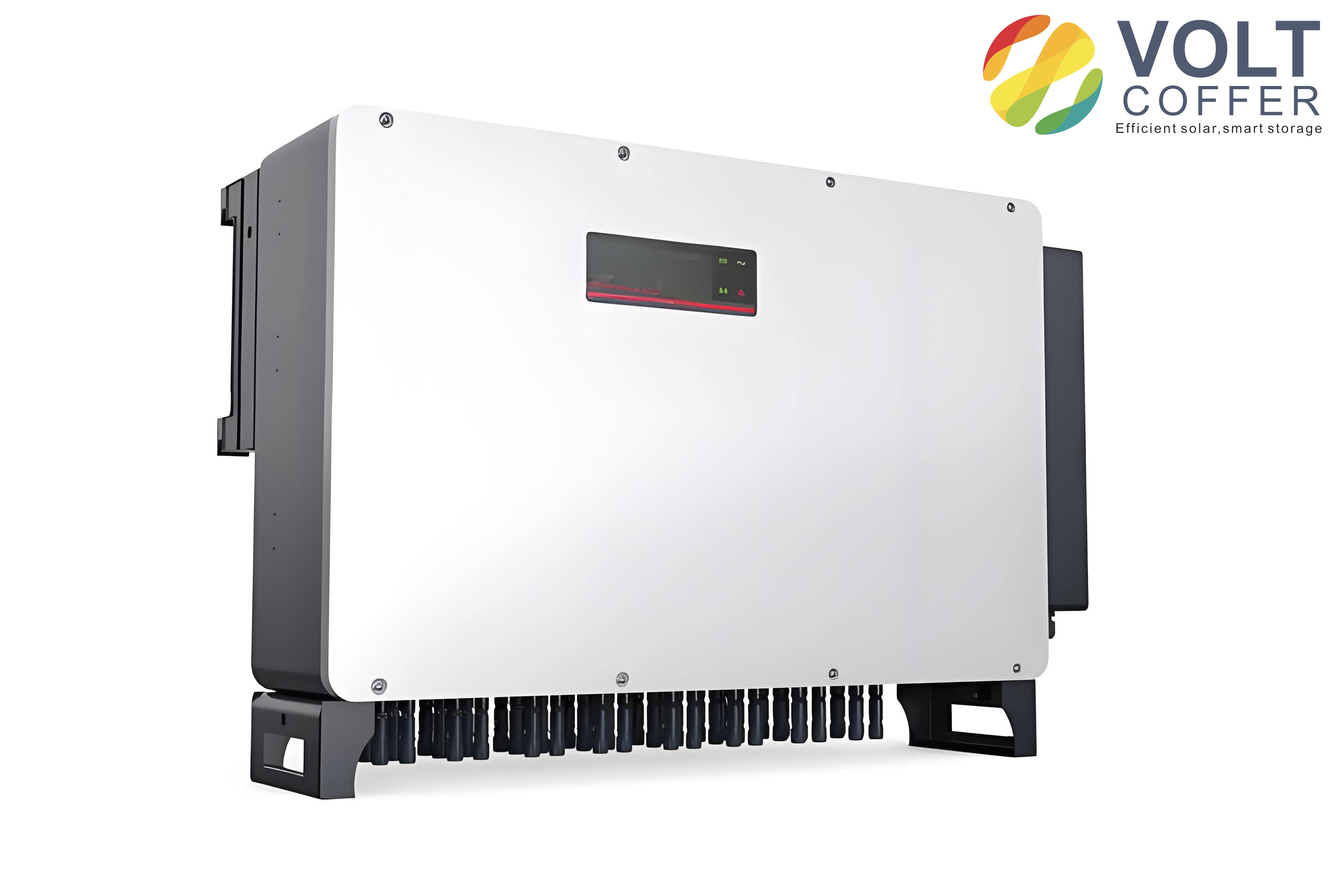
This image illustrates the experimental setup of our micro solar inverter system, including the DC power supply, the inverter prototype, the DSP controller, and the load. The compact structure enabled by GaN HEMT and the novel topology is evident.
2. Proposed ESL‑qZSI Topology
2.1 Circuit Configuration and Operating Modes
The ESL‑qZSI topology is shown schematically in the original paper (Figure 1). It consists of a DC input source, an auxiliary boost unit, an enhanced switched‑inductor boost unit combined with a quasi‑Z‑source network, followed by a single‑phase inverter bridge and an LC filter. Five diodes (D₁–D₅), four inductors (L₁–L₄), and four capacitors (C₁–C₄) form the impedance network. The inverter operates in two states: shoot‑through (ST) and non‑shoot‑through (NST).
Shoot‑through state: Both switches in each leg (S₁ & S₃, S₂ & S₄) are turned on simultaneously. Diodes D₁ and D₅ are reverse‑biased, while D₂, D₃, and D₄ conduct. Capacitors C₁, C₂, and C₃ are connected in series to charge inductors L₂ and L₃; capacitor C₄ charges inductor L₄.
Non‑shoot‑through state: The inverter bridge is in the active switching state and supplies power to the AC load. Diodes D₁ and D₅ conduct, while D₂, D₃, and D₄ are off. The input source and inductor L₁ charge C₁ and C₄; the source together with L₁, L₂, C₂, L₃, and L₄ supplies the load; inductor L₄ charges capacitor C₃.
2.2 Voltage Gain and Boost Factor Derivation
Let \(V_{\text{in}}\) be the DC input voltage, \(V_{\text{PN}}\) the DC‑link voltage across the inverter bridge, and \(D\) the shoot‑through duty ratio. The switching period is \(T_s\). Applying the volt‑second balance principle to inductors L₁–L₄ yields the following capacitor voltages:
\[
\begin{aligned}
V_{C1} &= \frac{1}{1-D} V_{\text{in}}, \\
V_{C2} &= \frac{1}{1-3D} V_{\text{in}}, \\
V_{C3} &= \frac{2D}{1-4D+3D^2} V_{\text{in}}, \\
V_{C4} &= \frac{2}{1-3D} V_{\text{in}}.
\end{aligned}
\]
The DC‑link voltage is the sum of \(V_{C3}\) and \(V_{C4}\):
\[
V_{\text{PN}} = V_{C3} + V_{C4} = \frac{2}{1-4D+3D^2} V_{\text{in}}.
\]
Hence, the boost factor \(B\) of the proposed micro solar inverter is
\[
B = \frac{V_{\text{PN}}}{V_{\text{in}}} = \frac{2}{1-4D+3D^2}.
\]
The voltage gain \(G\) is defined as \(G = M \cdot B\), where \(M = 1-D\) is the modulation index. Substituting \(M\) gives
\[
G = \frac{2}{3M-2}.
\]
Table 1 summarizes the key characteristics of the ESL‑qZSI topology.
| Parameter | Expression |
|---|---|
| Boost factor \(B\) | \(\displaystyle \frac{2}{1-4D+3D^2}\) |
| Voltage gain \(G\) | \(\displaystyle \frac{2}{3M-2}\) |
| Switch voltage stress \(V_{\text{sw}}/V_{\text{in}}\) | \(\displaystyle \frac{3G^2}{2G+2}\) |
| Capacitor C₁ stress \(V_{C1}/V_{\text{in}}\) | \(\displaystyle \frac{1}{1-D}\) |
| Capacitor C₂ stress \(V_{C2}/V_{\text{in}}\) | \(\displaystyle \frac{1}{1-3D}\) |
| Capacitor C₃ stress \(V_{C3}/V_{\text{in}}\) | \(\displaystyle \frac{2D}{1-4D+3D^2}\) |
| Capacitor C₄ stress \(V_{C4}/V_{\text{in}}\) | \(\displaystyle \frac{2}{1-3D}\) |
| Diode D₁/D₂ stress \(V_D/V_{\text{in}}\) | \(\displaystyle \frac{2}{1-4D+3D^2}\) |
| Diode D₃/D₄/D₅ stress \(V_D/V_{\text{in}}\) | \(\displaystyle \frac{1-D}{1-4D+3D^2}\) |
3. Performance Comparison with Existing Topologies
3.1 Boost Factor and Voltage Gain
We compare the proposed ESL‑qZSI, SL‑ZSI, and SLC‑qZSI. Their boost factors are:
\[
\begin{aligned}
B_{\text{SL‑ZSI}} &= \frac{1+D}{1-3D}, \\
B_{\text{SLC‑qZSI}} &= \frac{1}{1-4D}, \\
B_{\text{ESL‑qZSI}} &= \frac{2}{1-4D+3D^2}.
\end{aligned}
\]
At a shoot‑through duty ratio \(D=0.2\) (i.e., \(M=0.8\)), the theoretical boost factors are: \(B_{\text{SL‑ZSI}}=3\), \(B_{\text{SLC‑qZSI}}=5\), and \(B_{\text{ESL‑qZSI}}=6.25\). The corresponding voltage gains are: \(G_{\text{SL‑ZSI}}=2.4\), \(G_{\text{SLC‑qZSI}}=4\), and \(G_{\text{ESL‑qZSI}}=5\). Our proposed micro solar inverter thus achieves 108 % higher boost factor than SL‑ZSI and 25 % higher than SLC‑qZSI.
3.2 Voltage Stress on Switching Devices
Expressing the switch voltage stress \(V_{\text{sw}}\) as a function of the voltage gain \(G\):
\[
\begin{aligned}
V_{\text{sw,SL‑ZSI}} &= \frac{2G}{2-3G+\sqrt{9G^2-4G+4}} V_{\text{in}}, \\
V_{\text{sw,SLC‑qZSI}} &= \frac{4G-1}{3} V_{\text{in}}, \\
V_{\text{sw,ESL‑qZSI}} &= \frac{3G^2}{2G+2} V_{\text{in}}.
\end{aligned}
\]
The ESL‑qZSI exhibits the lowest switch voltage stress for a given gain, which improves thermal management and reliability of the micro solar inverter.
4. GaN HEMT Selection and Gate Driver Design
For the prototype, we selected the Infineon CoolGaN IGOT60R070D1 device, which has a 600 V breakdown voltage, 31 A continuous drain current, and an on‑resistance of 70 mΩ. To achieve reliable high‑frequency operation at 100 kHz, we designed a dedicated negative‑voltage turn‑off gate driver based on the 1EDF5673K driver IC. The driver circuit uses a buck‑type negative bias supply to provide a negative voltage during turn‑off, effectively suppressing the Miller‑effect induced parasitic turn‑on.
Table 2 lists the optimized key parameters of the gate driver.
| Parameter | R₇ (Ω) | R₅ (Ω) | R₄ (Ω) | C₆ (nF) | C₃ (nF) | C₄ (nF) |
|---|---|---|---|---|---|---|
| Value | 470 | 10 | 3.3 | 3 | 100 | 1 |
The use of GaN HEMT allows the micro solar inverter to operate at 100 kHz—ten times higher than the typical 10 kHz used in silicon‑based designs. This frequency increase reduces the required inductance values and capacitor sizes, leading to a more compact overall system.
5. Simulation and Experimental Results
5.1 Simulation Validation
We built a MATLAB/Simulink model of the ESL‑qZSI with the parameters listed in Table 3. The single‑phase SVPWM control scheme was implemented.
| Parameter | Value |
|---|---|
| Input voltage \(V_{\text{in}}\) | 64 V |
| Switching frequency | 100 kHz |
| QZS network capacitors (C₁–C₄) | 100 μF each |
| QZS network inductors (L₁–L₄) | 0.5 mH each |
| LC filter capacitor | 20 μF |
| LC filter inductor | 1 mH |
| Shoot‑through duty ratio \(D\) | 0.2 |
| Fundamental frequency | 50 Hz |
The simulated DC‑link voltage reached 380 V, corresponding to a boost factor of 5.94 (slightly lower than the theoretical 6.25 due to non‑idealities). The filtered output voltage amplitude was 294 V, giving a voltage gain of 4.59. The THD was 1.69 %, well below the typical grid‑tied standard of 5 %.
Capacitor voltage stresses were also simulated: C₄ had the highest stress around 300 V, C₂ about 150 V, and C₁ and C₃ about 80 V, matching the theoretical predictions.
5.2 Experimental Verification
We fabricated a prototype ESL‑qZSI micro solar inverter based on GaN HEMT. The experimental setup consisted of the inverter board, a TMS320F28335 DSP controller, a DC power supply, a resistive load, and an oscilloscope.
The gate‑driver output waveform measured at 100 kHz showed clean switching with a peak voltage of 3.4 V. The DC‑link voltage was measured as 368 V, yielding a practical boost factor of 5.75. The output voltage waveform was a smooth sinusoid with an amplitude of 272 V (RMS 188 V) at 50 Hz, with an output power of 180 W and an efficiency of 90.5 %. Fast Fourier transform (FFT) analysis of the output voltage revealed a THD of 2.57 %, satisfying the grid interconnection requirements.
Table 4 compares our experimental results with those reported for other micro solar inverter topologies under similar operating conditions.
| Parameter | SL‑ZSI (theoretical) | SLC‑qZSI (exp.) | This work ESL‑qZSI (exp.) |
|---|---|---|---|
| Input voltage \(V_{\text{in}}\) | 36 V | 80 V | 64 V |
| Shoot‑through duty \(D\) | 0.2 | 0.206 | 0.2 |
| Modulation index \(M\) | 0.8 | 0.794 | 0.8 |
| Boost factor \(B\) | 3 | 5 | 5.75 |
| Switching frequency | 10 kHz | 13.3 kHz | 100 kHz |
| Efficiency | — | 88.5 % | 90.5 % |
Our micro solar inverter achieves a 15 % higher boost factor than the SLC‑qZSI and a 91 % higher boost factor than the theoretical SL‑ZSI, while operating at a much higher switching frequency and with improved efficiency.
6. Conclusion
In this work, we have proposed, analyzed, and experimentally demonstrated a novel GaN‑based micro solar inverter employing an enhanced switched‑inductor quasi‑Z‑source topology. The auxiliary boost unit integrated with the switched‑inductor network significantly elevates the voltage gain at low shoot‑through duty ratios and lowers the voltage stress on the power switches. By leveraging GaN HEMT technology and a dedicated negative‑voltage gate driver, we increased the switching frequency to 100 kHz, reducing passive component size. The prototype delivered a boost factor of 5.75 at \(D=0.2\), outperforming existing topologies, and achieved a peak efficiency of 90.5 % with a THD of 2.57 %. These results confirm that the proposed micro solar inverter is a promising candidate for high‑performance, compact distributed photovoltaic systems, particularly in residential and commercial applications where high step‑up ratio and reliability are paramount.