
Perovskite solar cells have garnered significant attention in the scientific community due to their advantages in cost, light absorption properties, carrier transport characteristics, and exciton lifetime, positioning them at the forefront of next-generation thin-film solar cell research. Over the past decade, the certified power conversion efficiency (PCE) of perovskite solar cells has rapidly increased from 3.8% to 26.1%. However, these high efficiencies are primarily achieved in small-area devices (~0.1 cm²), while the development of large-area perovskite solar modules (PSMs) lags behind, with unsatisfactory progress. A major reason for the lower efficiency of PSMs is the complex fabrication process of perovskite thin films, which often requires additional steps such as anti-solvent treatment and annealing, making it challenging to produce uniform large-area perovskite films. Therefore, enhancing the film uniformity and PCE of large-area PSMs is a critical research focus for transitioning perovskite solar cells from laboratory-scale production to commercial applications.
Traditional methods for preparing small-area perovskite films typically involve anti-solvent treatment. However, parameters such as the type, amount, dripping rate, and timing of the anti-solvent significantly impact the quality of perovskite film formation, making it difficult to optimize processes suitable for various large-area film preparations. Consequently, ensuring reproducibility and controllability when scaling up perovskite film fabrication from laboratory to industrial production remains a challenge. A viable solution is to replace non-volatile solvents with volatile solvents (e.g., methylamine/acetonitrile, MA/ACN). Volatile solvents, characterized by high vapor pressure and low boiling points, can rapidly evaporate on their own after forming a liquid film, enabling uniform film formation without additional post-treatment processes. This greatly simplifies the工艺流程 and is more suitable for industrial production. However, perovskite films prepared using volatile solvent systems often exhibit excessively fast crystallization rates, resulting in smaller perovskite grain sizes and higher defect state densities in the films. This leads to increased non-radiative recombination, potentially causing poorer device efficiency and stability.
In this study, we designed a volatile solvent system composed of methylamine/acetonitrile (MA/ACN) to fabricate MAPbI3 perovskite solar cells and modules. An optimal amount of PbCl2 was added to the perovskite precursor solution to retard crystallization and passivate grain boundary defects. The small-area devices (0.06 cm²) fabricated using this method achieved a maximum PCE of 21.21%, along with improved stability. Furthermore, the perovskite solar cell modules prepared based on this process reached a PCE of 18.89%. This research provides a new approach for the large-scale industrial production of perovskite solar cells.
The perovskite precursor solution was prepared by weighing 0.1590 g of MAI and 0.4610 g of PbI2 (molar ratio 1:1), with the addition of PbCl2 at molar percentages of 0, 2.5%, 5%, and 7.5%. The mixture was dissolved in 1 mL of a MA/ACN mixed solvent (volume ratio 1:1) under magnetic stirring for 1 hour to obtain a 1 mol/L perovskite precursor solution. The resulting perovskite films were named PVK-0PbCl2, PVK-2.5PbCl2, PVK-5PbCl2, and PVK-7.5PbCl2 based on the PbCl2 content, and the corresponding devices were labeled PSC-0PbCl2, PSC-2.5PbCl2, PSC-5PbCl2, and PSC-7.5PbCl2.
For the electron transport layer, a chemical bath solution was prepared by adding 2.5 mL of hydrochloric acid, 50 μL of thioglycolic acid, 2.5 g of urea, and 0.548 g of SnCl2·2H2O to 200 mL of deionized water, followed by thorough stirring. Additionally, a SnO2 colloid solution was obtained by diluting a 15 wt% tin oxide hydrogel to 2.5 wt% with deionized water. The perovskite solar cells were fabricated on FTO glass substrates, which were cleaned with deionized water, acetone, isopropanol, and ethanol, then dried with N2 gas and treated with UV ozone for 15 minutes to remove residual organic contaminants. The SnO2 electron transport layer was deposited using a combination of chemical bath deposition and spin-coating methods. The FTO glass was immersed in the chemical bath solution at 90°C for 4 hours, followed by ultrasonication for 10 minutes to remove residual SnO2 particles, and then annealed at 180°C for 60 minutes. After UVO treatment for 15 minutes, the 2.5 wt% SnO2 colloid solution was spin-coated at 5000 rpm for 30 seconds and annealed at 150°C for 30 minutes. The substrate was further treated with UVO for 15 minutes before transferring to an N2 glovebox, where 25 μL of the perovskite precursor solution was dynamically spin-coated at 4000 rpm for 30 seconds to form the perovskite layer. The Spiro-OMeTAD solution (72.3 mg Spiro-OMeTAD, 29 μL 4-tert-butylpyridine, 18 μL lithium bis(trifluoromethanesulfonyl)imide, 1 mL chlorobenzene) was spin-coated at 4000 rpm for 30 seconds to form the hole transport layer. After oxidation in dry air for 8 hours, an 80–100 nm thick gold electrode with an area of 0.06 cm² was deposited via thermal evaporation through a mask.
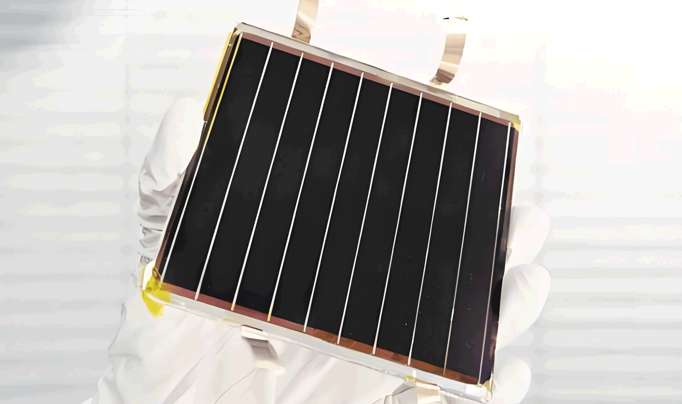
For the perovskite solar modules, a series-connected structure was fabricated on 5 cm × 5 cm FTO glass through a sequence of thin-film deposition and laser etching steps. A nanosecond laser with a wavelength of 532 nm and power of 5 W was used for laser etching. The P1 line was etched to define the sub-cell width and cut the FTO glass. The SnO2 electron transport layer, perovskite layer, and hole transport layer were deposited under the same conditions as the small-area devices. The P2 line was etched to remove the deposited films on the FTO, allowing subsequent connection with the gold electrode. After gold electrode deposition, the P3 line was etched to remove the gold electrode and other layers except the FTO, forming a series-connected structure. The module consisted of six series-connected sub-cells, each with a width of 6.5 mm and a length of 40 mm.
To investigate the effect of PbCl2 addition on the surface morphology of perovskite films, scanning electron microscopy (SEM) images of PVK-0PbCl2 and PVK-5PbCl2 were recorded, and energy-dispersive X-ray spectroscopy (EDS) was used to analyze the elemental content of PVK-5PbCl2. The SEM images revealed uniform and dense morphologies without pinholes for both films. Additionally, PVK-5PbCl2 exhibited larger and more uniformly distributed grain sizes, attributed to the higher bond energy of Pb–Cl compared to Pb–I, which slows down the crystallization rate of MAPbI3, leading to larger perovskite grains. The EDS elemental mapping showed negligible Cl content in PVK-5PbCl2, as Cl volatilizes in the form of MACl during crystallization, while excess Pb exists as PbI2 in the film and enriches at the grain boundaries. Statistical analysis of grain sizes from SEM images indicated average grain sizes of 180 nm for PVK-0PbCl2 and 253 nm for PVK-5PbCl2.
X-ray diffraction (XRD) and UV-Vis absorption spectroscopy were employed to study the crystallinity and bandgap changes of the films. The XRD patterns of both PVK-0PbCl2 and PVK-5PbCl2 showed typical MAPbI3 perovskite crystal structures, with prominent diffraction peaks at 2θ = 14.14°, 28.52°, and 43.22°, corresponding to the (110), (220), and (330) crystal planes, respectively. The diffraction peaks of PVK-5PbCl2 were significantly stronger than those of PVK-0PbCl2, indicating better crystallinity, consistent with the SEM results. The UV-Vis absorption spectra showed that the absorption edges of both films were around 783 nm, corresponding to a bandgap of 1.584 eV, suggesting that the addition of PbCl2 does not significantly affect the film bandgap.
To evaluate the impact of PbCl2 on the photovoltaic properties of perovskite films, photoluminescence (PL) spectra, time-resolved photoluminescence (TRPL) spectra, space-charge-limited current (SCLC) curves, dark J–V curves, conductivity, and electrochemical impedance spectroscopy (EIS) were measured. The PL spectra showed that both films had PL peaks at 756 nm, but the PL intensity of PVK-5PbCl2 was significantly enhanced, indicating suppressed non-radiative recombination at grain boundaries due to PbI2 enrichment. TRPL spectra were fitted using a bi-exponential decay model to assess carrier lifetime. The average fluorescence decay lifetime (τave) was calculated using the formula:
$$ \tau_{\text{ave}} = \frac{A_1 \tau_1^2 + A_2 \tau_2^2}{A_1 \tau_1 + A_2 \tau_2} $$
where A1 and A2 are the decay amplitudes, and τ1 and τ2 are the fast and slow decay time constants, respectively. The average carrier lifetime for PVK-5PbCl2 was 644.1 ns, compared to 240.6 ns for PVK-0PbCl2, indicating longer carrier diffusion lengths and more efficient charge transport in PVK-5PbCl2.
SCLC measurements were used to characterize the defect density (Nt) and charge mobility of the films. The defect density was calculated using the formula:
$$ N_t = \frac{2 \varepsilon_0 \varepsilon_r V_{\text{TFL}}}{e L^2} $$
where e is the elementary charge, ε0 is the vacuum permittivity, εr is the relative permittivity of MAPbI3 (εr = 32), L is the perovskite layer thickness (650 nm), and VTFL is the trap-filling limit voltage. The VTFL values were 0.142 V for PVK-0PbCl2 and 0.120 V for PVK-5PbCl2, resulting in Nt values of 1.19 × 1015 cm−3 and 1.01 × 1015 cm−3, respectively. The electron mobility (μ) was estimated in the trap-free region (n = 2) using the formula:
$$ \mu = \frac{8 J_D L^3}{9 \varepsilon_0 \varepsilon_r V_b^2} $$
where JD is the dark current density and Vb is the applied voltage. The electron mobility of PVK-5PbCl2 was 4.38 × 10⁻¹ cm²/(V·s), an order of magnitude higher than that of PVK-0PbCl2 (4.06 × 10⁻² cm²/(V·s)). Dark J–V curves showed that the leakage current of PVK-5PbCl2 (6.57 × 10⁻⁵ mA/cm²) was significantly lower than that of PVK-0PbCl2 (8.60 × 10⁻⁴ mA/cm²), confirming the passivation effect of PbCl2. Conductivity measurements revealed that PVK-5PbCl2 had a higher conductivity (6.16 × 10⁻⁵ S/cm) than PVK-0PbCl2 (4.75 × 10⁻⁵ S/cm). EIS Nyquist plots fitted with an equivalent circuit model showed lower charge transfer resistance for PSC-5PbCl2 (3.18 × 10² kΩ) compared to PSC-0PbCl2 (4.09 × 10² kΩ), indicating enhanced charge transfer and suppressed interface recombination.
The photovoltaic performance of perovskite solar cells with different PbCl2 additions was evaluated through J–V measurements. The champion device PSC-5PbCl2 achieved a PCE of 21.21%, with a fill factor (FF) of 79.70%, open-circuit voltage (VOC) of 1.08 V, and short-circuit current density (JSC) of 24.72 mA/cm². In comparison, PSC-0PbCl2 had a PCE of 19.31%, FF of 77.40%, VOC of 1.02 V, and JSC of 24.35 mA/cm². External quantum efficiency (EQE) measurements integrated to a current density of 24.12 mA/cm² for PSC-5PbCl2, consistent with the J–V results. Electroluminescence EQE (EQEEL) analysis showed a lower open-circuit voltage loss for PSC-5PbCl2 (0.226 V) compared to PSC-0PbCl2 (0.268 V). Steady-state power output (SPO) measurements at 0.88 V bias yielded a stable PCE of 21.16% for PSC-5PbCl2. Stability tests under ambient conditions (room temperature, humidity <10%) demonstrated that PSC-5PbCl2 retained over 90% of its initial PCE after 500 hours, while PSC-0PbCl2 retained only 78.92%.
For the perovskite solar modules, the geometric fill factor (GFF) was approximately 95.4%, with a total active area of 14.88 cm². The champion module achieved a PCE of 18.89%, with a maximum output power of 280.61 mW, FF of 73.69%, short-circuit current (ISC) of 58.67 mA, and open-circuit voltage (VOC) of 6.50 V. The module successfully powered 100 LED bulbs under operating conditions. SPO measurements at 4.90 V bias showed a stable output current of 56.85 mA. To assess film uniformity, a 5 cm × 5 cm large-area perovskite film was divided into 16 sections for UV-Vis and XRD analysis. The consistency in absorption spectra and diffraction peak intensities confirmed high film homogeneity. The radial grain size deviation, calculated using the Scherrer equation, was below 10%. Photoluminescence intensity mapping and SEM images from various positions on the film further verified uniform morphology and thickness (~650 nm).
In conclusion, this study presents a method for fabricating high-efficiency MAPbI3 perovskite solar cells and modules using volatile solvents. The addition of PbCl2 retards crystallization, leading to larger perovskite grains and passivated grain boundaries. The champion small-area device achieved a PCE of 21.21%, with improved steady-state output and stability. The large-area module attained a PCE of 18.89%, demonstrating the scalability of this approach. This work offers a simplified工艺 for producing high-performance, large-area perovskite solar modules, advancing the industrialization of perovskite solar cells.
| Sample | PCE (%) | FF (%) | VOC (V) | JSC (mA/cm²) |
|---|---|---|---|---|
| PSC-0PbCl2 (Average) | 18.26 | 74.26 | 1.04 | 23.48 |
| PSC-0PbCl2 (Champion) | 19.31 | 77.40 | 1.02 | 24.35 |
| PSC-2.5PbCl2 (Average) | 19.11 | 75.87 | 1.07 | 23.65 |
| PSC-2.5PbCl2 (Champion) | 20.17 | 76.70 | 1.08 | 24.03 |
| PSC-5PbCl2 (Average) | 20.35 | 77.72 | 1.08 | 24.20 |
| PSC-5PbCl2 (Champion) | 21.21 | 79.70 | 1.08 | 24.72 |
| PSC-7.5PbCl2 (Average) | 19.23 | 76.25 | 1.07 | 23.61 |
| PSC-7.5PbCl2 (Champion) | 20.37 | 78.10 | 1.08 | 24.21 |
| Sample | Defect Density (cm−3) | Electron Mobility (cm²/(V·s)) |
|---|---|---|
| PVK-0PbCl2 | 1.19 × 10¹⁵ | 4.06 × 10⁻² |
| PVK-5PbCl2 | 1.01 × 10¹⁵ | 4.38 × 10⁻¹ |
| Reference | Year | PCEPSC (%) | PCEPSM (%) |
|---|---|---|---|
| This work | 2024 | 21.21 | 18.89 |
| Previous study A | 2022 | 19.14 | 17.12 |
| Previous study B | 2023 | 21.04 | 19.03 |
The development of perovskite solar cells continues to evolve, with volatile solvent systems playing a crucial role in simplifying fabrication processes for large-scale production. The incorporation of additives like PbCl2 not only enhances crystallinity and reduces defects but also improves the overall performance and stability of perovskite solar cells. Future work should focus on optimizing solvent compositions and additive concentrations to further push the boundaries of efficiency and scalability in perovskite photovoltaics.