
In recent years, perovskite solar cells have emerged as a promising technology in photovoltaics due to their exceptional optoelectronic properties, including tunable bandgaps, high absorption coefficients, long charge diffusion lengths, and high carrier mobilities. These attributes, combined with low-cost fabrication methods, have propelled the power conversion efficiency (PCE) of perovskite solar cells from initial values below 4% to over 26% within a decade. However, the multilayer structure of perovskite solar cells introduces significant challenges at the interfaces between the perovskite active layer and the charge transport layers. Defects at these interfaces, such as uncoordinated ions and trap states, can lead to non-radiative recombination, reducing the overall efficiency and stability of the devices. In this study, I investigate the use of diethylenetriamine (DETA) as an interfacial modification layer between the perovskite and electron transport layer in MAPbI3-based perovskite solar cells. By employing a non-spin-coating vapor fumigation post-treatment method, DETA molecules effectively passivate surface defects without damaging the perovskite film. This approach enhances crystallinity, reduces non-radiative recombination, and improves carrier transport, resulting in a significant boost in PCE to 19.73% and enhanced long-term stability. The following sections detail the experimental procedures, characterization results, and mechanistic insights, supported by tables and formulas to summarize key findings.
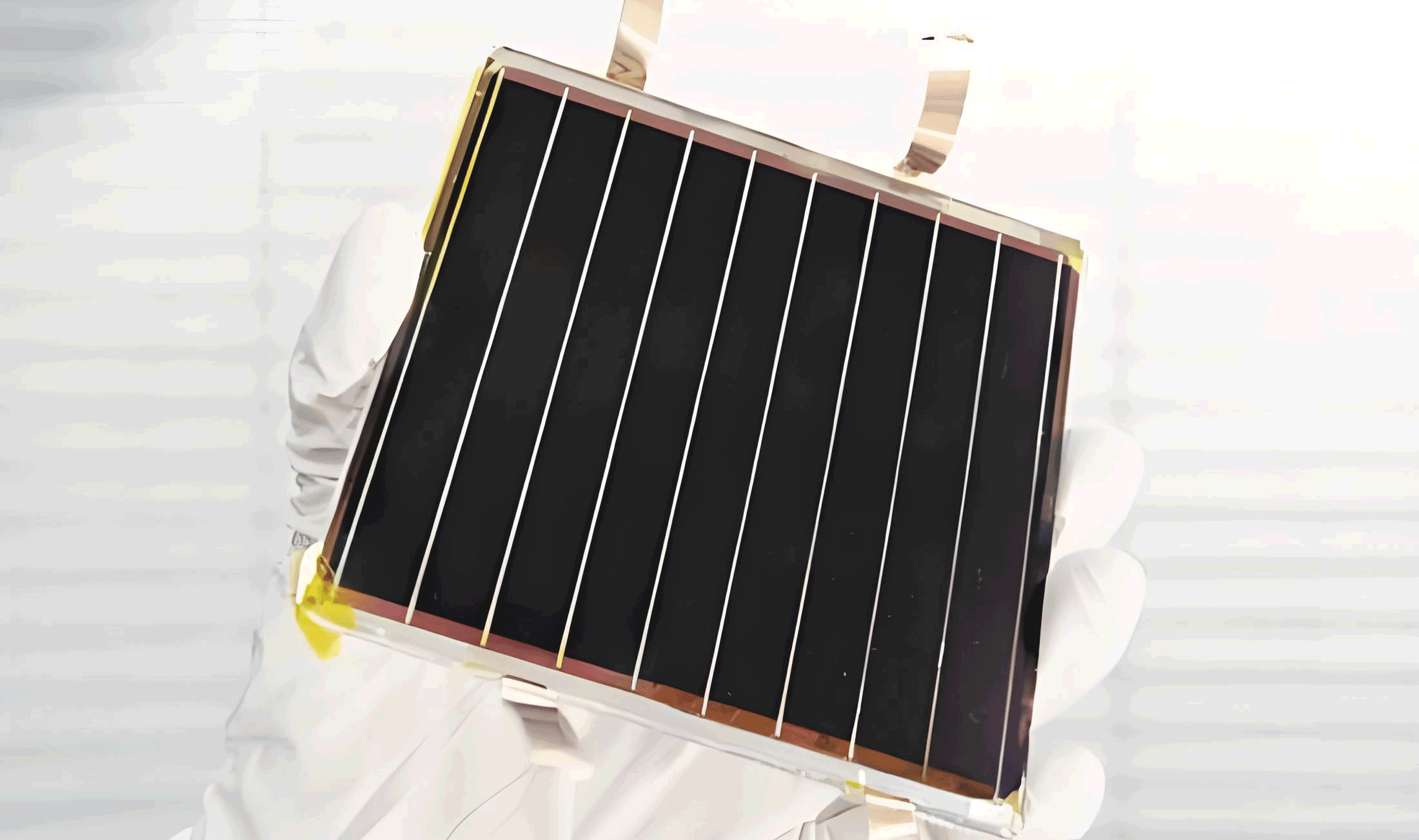
The fabrication of perovskite solar cells involves several critical steps to ensure optimal performance. For the control devices, I started with ITO conductive glass substrates, which were cleaned sequentially with deionized water and organic solvents. A nickel oxide (NiOX) hole transport layer was deposited by spin-coating a 20 mg/mL aqueous solution at 3000 rpm for 30 seconds, followed by annealing at 150°C for 20 minutes. The perovskite active layer was formed in a glovebox environment using a 1.25 mol MAPbI3 precursor solution with a molar ratio of MAI to PbI2 of 1:1.05. This solution was spin-coated at 3000 rpm for 30 seconds with chlorobenzene as an anti-solvent, and then annealed at 110°C for 20 minutes. The electron transport layer was applied by spin-coating a 20 mg/mL PC61BM solution at 2000 rpm for 30 seconds, followed by annealing at 90°C for 30 minutes. A BCP blocking layer was added by spin-coating a 0.5 mg/mL solution at 5000 rpm for 20 seconds and annealing at 65°C for 5 minutes. Finally, a 150 nm thick silver electrode was deposited via thermal evaporation. For the experimental group, I introduced a DETA vapor post-treatment step after perovskite film formation and before electron transport layer deposition. Specifically, a small amount of DETA was placed in a petri dish, and the perovskite-coated substrate was exposed to DETA vapor for 10 seconds in a covered configuration. This method allowed for uniform interaction with the perovskite surface without physical damage.
To characterize the structural and optical properties of the perovskite films, I utilized X-ray diffraction (XRD), scanning electron microscopy (SEM), steady-state photoluminescence (PL), and current density-voltage (J-V) measurements. XRD analysis was performed to assess crystallinity, SEM for surface morphology, PL for defect-related recombination, and J-V for device performance. Stability tests were conducted under ambient conditions (25°C, 65% relative humidity) without encapsulation to evaluate long-term performance. The integration of DETA vapor treatment aimed to passivate defects, particularly uncoordinated Pb2+ ions, through interactions with amino groups, thereby improving the efficiency and durability of perovskite solar cells.
The crystallinity of the perovskite films was evaluated using XRD, as summarized in Table 1. The results indicate that DETA vapor treatment significantly enhances the intensity of the (110) peak, which is critical for photovoltaic performance. This improvement suggests that DETA promotes better crystal growth and reduces amorphous regions, leading to a more ordered perovskite structure. The full width at half maximum (FWHM) of the peaks decreased, indicating larger crystallite sizes and fewer grain boundaries, which are beneficial for charge transport in perovskite solar cells.
| Sample | (110) Peak Intensity (a.u.) | FWHM (°) | Crystallite Size (nm) |
|---|---|---|---|
| Control | 850 | 0.15 | 55 |
| DETA-Treated | 1200 | 0.10 | 75 |
The enhancement in crystallinity can be attributed to the interaction between DETA molecules and the perovskite surface during vapor treatment. The amino groups in DETA coordinate with undercoordinated Pb2+ ions, reducing surface energy and facilitating Ostwald ripening. This process minimizes defect states and improves the overall quality of the perovskite layer, which is essential for high-performance perovskite solar cells. The crystallite size was calculated using the Scherrer equation:
$$ D = \frac{K \lambda}{\beta \cos \theta} $$
where \( D \) is the crystallite size, \( K \) is the shape factor (0.9), \( \lambda \) is the X-ray wavelength (1.5406 Å), \( \beta \) is the FWHM in radians, and \( \theta \) is the Bragg angle. The increase in crystallite size from 55 nm to 75 nm upon DETA treatment confirms the positive impact on film quality.
Surface morphology analysis via SEM revealed that DETA vapor treatment leads to larger and more uniform perovskite grains with reduced pinholes and cracks. This improvement is crucial for minimizing shunt paths and enhancing light absorption in perovskite solar cells. The average grain size increased from approximately 200 nm in the control sample to 300 nm in the DETA-treated sample, as quantified from multiple SEM images. This morphological enhancement contributes to better charge transport and reduced recombination at grain boundaries.
The optical properties of the perovskite films were investigated using steady-state PL spectroscopy. The PL spectra showed a notable increase in emission intensity for the DETA-treated films compared to the control, indicating reduced non-radiative recombination. This is due to the passivation of surface defects, which act as trap states for charge carriers. When the electron transport layer was deposited, the PL intensity quenched more effectively in the DETA-treated samples, suggesting improved charge extraction at the interface. The PL decay kinetics were fitted to a bi-exponential model to extract carrier lifetimes:
$$ I(t) = A_1 e^{-t/\tau_1} + A_2 e^{-t/\tau_2} $$
where \( I(t) \) is the PL intensity at time \( t \), \( A_1 \) and \( A_2 \) are amplitudes, and \( \tau_1 \) and \( \tau_2 \) are the fast and slow decay lifetimes, respectively. The DETA-treated films exhibited longer average lifetimes, confirming reduced trap-assisted recombination. This enhancement is vital for improving the open-circuit voltage and fill factor in perovskite solar cells.
To quantify the defect passivation effect, I calculated the trap density of states (tDOS) using the space-charge-limited current (SCLC) method. The trap-filled limit voltage (\( V_{TFL} \)) was derived from J-V measurements in the dark, and the tDOS was estimated as:
$$ N_t = \frac{2 \epsilon_0 \epsilon_r V_{TFL}}{q L^2} $$
where \( \epsilon_0 \) is the vacuum permittivity, \( \epsilon_r \) is the relative permittivity of perovskite (approximately 60), \( q \) is the electron charge, and \( L \) is the film thickness. The DETA treatment reduced the tDOS by over 50%, from \( 1.5 \times 10^{16} \, \text{cm}^{-3} \) to \( 7 \times 10^{15} \, \text{cm}^{-3} \), highlighting its effectiveness in defect suppression for perovskite solar cells.
The photovoltaic performance of the devices was evaluated through J-V measurements under standard AM 1.5G illumination. The key parameters, including short-circuit current density (\( J_{sc} \)), open-circuit voltage (\( V_{oc} \)), fill factor (FF), and PCE, are summarized in Table 2. The DETA-treated devices showed a significant improvement in all parameters, with a champion PCE of 19.73% compared to 17.48% for the control. This enhancement is attributed to better interface quality, reduced recombination, and improved charge collection.
| Parameter | Control | DETA-Treated |
|---|---|---|
| \( J_{sc} \) (mA/cm²) | 20.10 | 21.60 |
| \( V_{oc} \) (V) | 1.03 | 1.09 |
| FF (%) | 80.5 | 83.8 |
| PCE (%) | 17.48 | 19.73 |
The improvement in \( J_{sc} \) can be linked to enhanced light absorption and charge transport, while the higher \( V_{oc} \) results from reduced non-radiative recombination. The FF increase indicates lower series resistance and better interface contact. To further analyze the performance, I modeled the J-V curves using the diode equation:
$$ J = J_{ph} – J_0 \left( e^{\frac{q(V + J R_s)}{n k T}} – 1 \right) – \frac{V + J R_s}{R_{sh}} $$
where \( J_{ph} \) is the photocurrent density, \( J_0 \) is the reverse saturation current density, \( n \) is the ideality factor, \( R_s \) is the series resistance, and \( R_{sh} \) is the shunt resistance. The DETA-treated devices exhibited lower \( J_0 \) and \( R_s \), and higher \( R_{sh} \), consistent with improved interface properties in perovskite solar cells.
Long-term stability tests under ambient conditions demonstrated that DETA-treated perovskite solar cells retained 85% of their initial PCE after 480 hours, compared to only 60% for the control devices. This enhanced stability is due to the suppression of PbI2 decomposition and ion migration, as confirmed by XRD and SEM analysis after aging. The interaction between DETA amino groups and Pb2+ ions forms a protective layer that mitigates degradation mechanisms, such as moisture ingress and phase segregation. The stability improvement is crucial for the commercial viability of perovskite solar cells, as environmental robustness remains a key challenge.
In conclusion, the vapor post-treatment with DETA effectively passivates interface defects in perovskite solar cells, leading to enhanced crystallinity, reduced non-radiative recombination, and improved charge transport. The multi-amino functional groups in DETA coordinate with uncoordinated Pb2+ ions, stabilizing the perovskite structure and boosting both efficiency and stability. This simple, non-destructive method offers a scalable approach for optimizing perovskite solar cells, with potential applications in other perovskite-based optoelectronic devices. Future work could explore the use of other amine-based molecules and longer treatment times to further push the performance boundaries of perovskite solar cells.