
Perovskite solar cells have emerged as a promising photovoltaic technology due to their high power conversion efficiency, low-cost fabrication, and solution-processability. In recent years, the efficiency of perovskite solar cells has rapidly increased from initial reports to over 26%, making them competitive with traditional silicon-based solar cells. However, the commercialization of perovskite solar cells faces challenges related to cost and long-term stability. One significant cost factor is the use of gold as the back electrode in conventional n-i-p structured perovskite solar cells. Gold offers excellent stability and suitable work function alignment with common hole transport materials, but its high price increases the overall manufacturing cost. To address this, silver has been proposed as a low-cost alternative due to its high electrical conductivity and relative affordability. Unfortunately, when silver is directly deposited on hole transport layers like spiro-MeOTAD, it often results in abnormal S-shaped current density-voltage (J-V) curves, which severely degrade the photovoltaic performance of perovskite solar cells. This S-shaped behavior is attributed to the formation of a Schottky barrier at the interface between the hole transport layer and the silver electrode, caused by a mismatch in work functions. Over time, a self-healing process can occur where silver reacts with additives in the hole transport layer, such as lithium bis(trifluoromethanesulfonyl)imide (Li-TFSI), forming Ag-TFSI complexes that modify the interface and restore normal J-V characteristics. However, this self-healing is unpredictable and not suitable for reliable manufacturing. Therefore, introducing a buffer layer between the hole transport layer and the silver electrode is a critical strategy to mitigate these issues and enhance both efficiency and stability of perovskite solar cells.
In this study, we investigate the use of molybdenum oxide (MoOx) as a buffer layer deposited via thermal evaporation between the spiro-MeOTAD hole transport layer and the silver back electrode in perovskite solar cells. The MoOx layer serves to improve hole transport properties, reduce charge recombination, and suppress detrimental reactions between silver and halide ions from the perovskite layer. We systematically vary the thickness of the MoOx layer and analyze its impact on the photovoltaic parameters, including power conversion efficiency (PCE), short-circuit current density (Jsc), open-circuit voltage (Voc), and fill factor (FF). Our results demonstrate that an optimal MoOx thickness eliminates the S-shaped J-V curves and significantly boosts the performance and longevity of silver-based perovskite solar cells. This approach not only addresses the interfacial issues but also provides a pathway for cost-effective and stable perovskite solar cell devices, which is essential for their large-scale deployment.
The fundamental operation of a perovskite solar cell relies on the efficient generation and extraction of charge carriers. When light is absorbed by the perovskite layer, electron-hole pairs are created. These carriers are then separated and transported to the respective electrodes through electron transport layers (ETLs) and hole transport layers (HTLs). In n-i-p structured perovskite solar cells, the hole transport layer plays a crucial role in extracting holes and blocking electrons. The interface between the hole transport layer and the electrode is critical for minimizing losses. The work function of the electrode material must align well with the highest occupied molecular orbital (HOMO) of the hole transport layer to facilitate efficient hole extraction. Silver has a work function of approximately 4.3 eV, while spiro-MeOTAD has a HOMO level around 5.2 eV. This mismatch creates a energy barrier, leading to increased series resistance and reduced fill factor, manifesting as S-shaped J-V curves. The current density-voltage relationship in such cases can be modeled using diode equations that account for series and shunt resistances. For instance, the ideal diode equation is given by:
$$ J = J_0 \left( \exp\left(\frac{q(V – J R_s)}{n k T}\right) – 1 \right) + \frac{V – J R_s}{R_{sh}} – J_{ph} $$
where \( J \) is the current density, \( J_0 \) is the reverse saturation current density, \( q \) is the electron charge, \( V \) is the voltage, \( R_s \) is the series resistance, \( R_{sh} \) is the shunt resistance, \( n \) is the ideality factor, \( k \) is Boltzmann’s constant, \( T \) is the temperature, and \( J_{ph} \) is the photocurrent density. In devices with interfacial barriers, \( R_s \) increases substantially, causing the S-shaped distortion. By introducing a MoOx buffer layer, which has a high work function (around 5.3-5.7 eV), we can better align the energy levels, reduce \( R_s \), and improve charge extraction. The enhanced interface also mitigates recombination losses, which can be described by the recombination current density:
$$ J_{rec} = J_{00} \exp\left(-\frac{E_a}{k T}\right) $$
where \( J_{00} \) is a prefactor and \( E_a \) is the activation energy for recombination. A lower \( J_{rec} \) contributes to higher Voc and FF in perovskite solar cells.
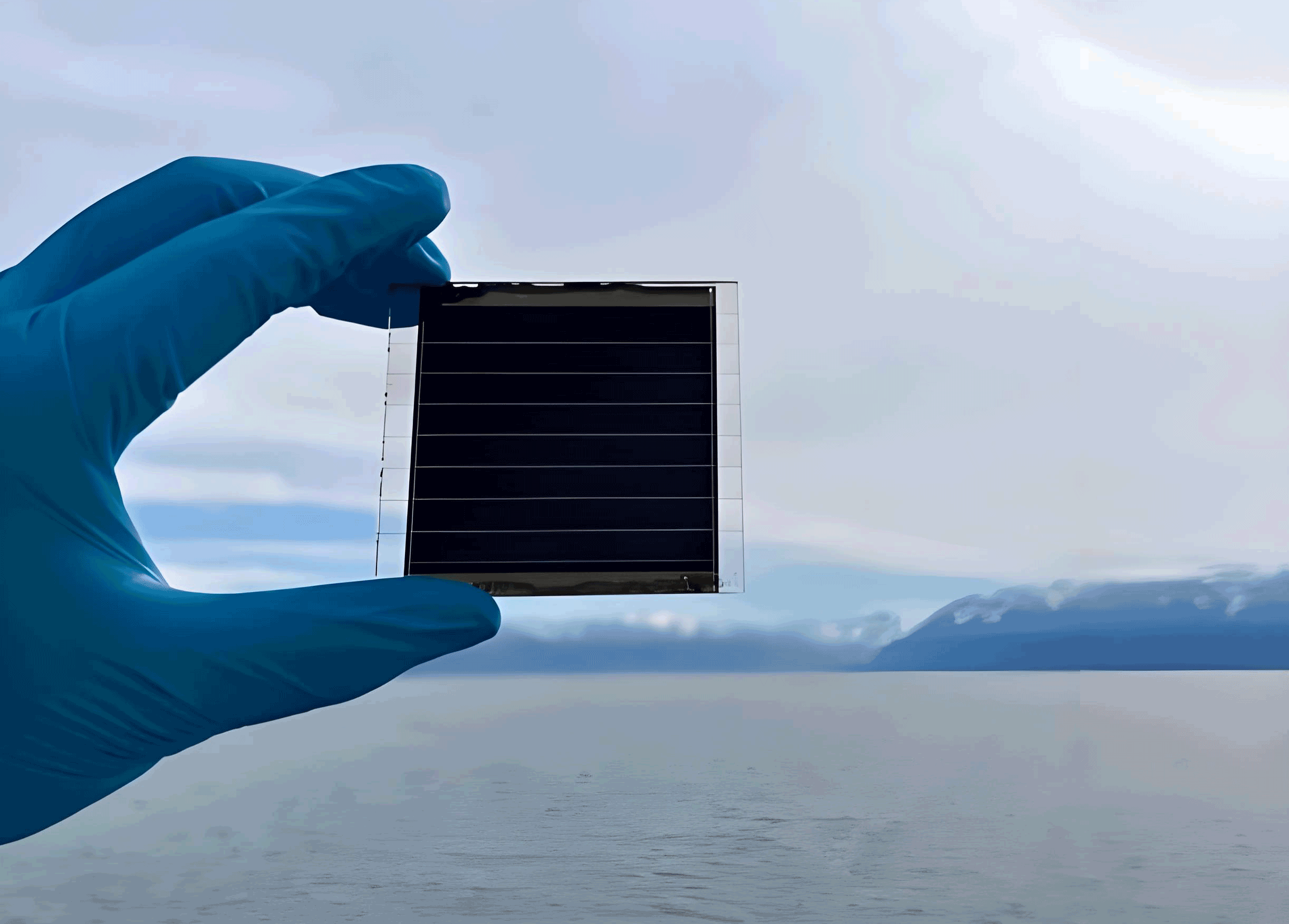
To fabricate the perovskite solar cells, we used fluorine-doped tin oxide (FTO) glass substrates that were cleaned and treated with ozone to remove organic residues. A compact tin oxide (SnO2) layer was deposited as the electron transport layer via spin-coating. The perovskite precursor solution was prepared by dissolving formamidinium iodide (FAI), lead iodide (PbI2), methylammonium bromide (MABr), and lead bromide (PbBr2) in a mixture of dimethylformamide (DMF) and dimethyl sulfoxide (DMSO), with the addition of cesium iodide (CsI) to form a triple-cation perovskite composition. The perovskite layer was deposited using a two-step spin-coating process with chlorobenzene as an anti-solvent, followed by annealing. The hole transport layer was formed by spin-coating a spiro-MeOTAD solution containing Li-TFSI and 4-tert-butylpyridine (TBP) additives. After oxidation, MoOx layers of varying thicknesses were deposited by thermal evaporation, followed by an 80 nm silver electrode. We prepared multiple devices for each condition to ensure statistical reliability.
The morphology and crystallinity of the perovskite films were characterized. The films exhibited uniform and pinhole-free surfaces, indicative of high-quality crystallization. X-ray diffraction patterns confirmed the formation of the desired perovskite phase without detectable impurities. Steady-state photoluminescence spectroscopy revealed enhanced quenching in samples with MoOx layers, suggesting improved charge extraction from the perovskite layer to the hole transport layer and electrode. This is consistent with reduced non-radiative recombination and better interface quality in perovskite solar cells.
We evaluated the photovoltaic performance of devices with different MoOx thicknesses under standard AM1.5G illumination. The J-V curves showed that without a MoOx layer, the devices exhibited pronounced S-shaped characteristics, leading to low fill factors and power conversion efficiencies. As the MoOx thickness increased, the S-shaped distortion diminished, and the performance improved up to an optimal thickness. Beyond this point, thicker MoOx layers increased series resistance and reduced performance. The external quantum efficiency (EQE) spectra indicated high response across the visible spectrum, with variations in the long-wavelength region due to optical interference effects from the MoOx layer. The stability tests demonstrated that devices with MoOx layers retained over 80% of their initial efficiency after 450 hours in ambient air, whereas reference devices degraded rapidly. This highlights the role of MoOx in protecting against moisture and ion diffusion, which are common degradation pathways in perovskite solar cells.
The following table summarizes the average photovoltaic parameters for perovskite solar cells with different MoOx layer thicknesses, based on statistical analysis of multiple devices:
| MoOx Thickness (nm) | PCE (%) | Jsc (mA/cm2) | Voc (V) | FF (%) |
|---|---|---|---|---|
| 0 | 13.2 | 22.5 | 1.14 | 52 |
| 3 | 14.8 | 23.1 | 1.15 | 56 |
| 6 | 16.5 | 23.4 | 1.16 | 61 |
| 9 | 18.7 | 23.8 | 1.18 | 66 |
| 15 | 17.2 | 23.5 | 1.17 | 63 |
| 25 | 15.9 | 23.2 | 1.16 | 59 |
| 35 | 14.5 | 22.9 | 1.15 | 55 |
The data clearly shows that the power conversion efficiency peaks at a MoOx thickness of 9 nm, with a 41% improvement over the reference device without MoOx. This enhancement is primarily due to increased fill factor and open-circuit voltage, resulting from reduced series resistance and better charge extraction. The short-circuit current density also improves slightly, attributed to enhanced light management and reduced recombination. The fill factor can be expressed as:
$$ FF = \frac{P_{max}}{J_{sc} \times V_{oc}} $$
where \( P_{max} \) is the maximum power output. Higher FF values indicate more square-like J-V curves, which is achieved with optimal MoOx thickness in perovskite solar cells.
To further understand the interfacial effects, we consider the energy level alignment. The work function of MoOx is around 5.5 eV, which bridges the gap between spiro-MeOTAD (HOMO ~5.2 eV) and silver (work function ~4.3 eV). This reduces the hole injection barrier and facilitates ohmic contact. The built-in potential (\( V_{bi} \)) across the device is enhanced, which drifts carriers more efficiently and increases Voc. The open-circuit voltage can be related to the quasi-Fermi level splitting:
$$ V_{oc} = \frac{1}{q} (E_{Fn} – E_{Fp}) $$
where \( E_{Fn} \) and \( E_{Fp} \) are the electron and hole quasi-Fermi levels, respectively. With better interface engineering, the quasi-Fermi level splitting is maximized, leading to higher Voc in perovskite solar cells.
Another critical aspect is the stability of perovskite solar cells. Silver electrodes are susceptible to reaction with iodide ions from the perovskite layer, forming silver iodide, which increases series resistance and degrades performance. The MoOx layer acts as a diffusion barrier, preventing this reaction. The degradation kinetics can be modeled by a diffusion-limited process:
$$ \frac{dC}{dt} = D \frac{d^2C}{dx^2} $$
where \( C \) is the concentration of diffusing species, \( D \) is the diffusion coefficient, and \( x \) is the position. By introducing a dense MoOx layer, the effective diffusion coefficient is reduced, slowing down the degradation. This is confirmed by our stability tests, where devices with MoOx maintained performance over time, unlike reference devices. The normalized PCE as a function of time follows an exponential decay in unstable devices, but remains stable with MoOx protection.
In addition to electrical and stability improvements, the optical properties of the MoOx layer contribute to enhanced performance in perovskite solar cells. MoOx has a high refractive index, which can modify the optical field distribution within the device. This can be analyzed using transfer matrix simulations to optimize light absorption. The photocurrent density is directly related to the absorption profile:
$$ J_{ph} = q \int \Phi(\lambda) EQE(\lambda) d\lambda $$
where \( \Phi(\lambda) \) is the photon flux and \( EQE(\lambda) \) is the external quantum efficiency. By tuning the MoOx thickness, we can achieve constructive interference that boosts EQE in specific wavelength ranges, particularly in the red and near-infrared regions where perovskite solar cells have strong absorption.
We also investigated the role of MoOx in reducing hysteresis in perovskite solar cells. Hysteresis in J-V curves is often linked to ion migration and interfacial trapping. The MoOx layer passivates the interface and reduces trap states, leading to more stable J-V characteristics. The hysteresis index (HI) can be defined as:
$$ HI = \frac{PCE_{reverse} – PCE_{forward}}{PCE_{reverse}} $$
where \( PCE_{reverse} \) and \( PCE_{forward} \) are power conversion efficiencies measured in reverse and forward voltage scans, respectively. Devices with MoOx layers exhibited lower hysteresis indices, indicating improved interfacial quality and reduced ion migration in perovskite solar cells.
Furthermore, we explored the impact of MoOx on the charge carrier dynamics using transient photovoltage and photocurrent measurements. The charge extraction time (\( \tau_{ext} \)) is shortened with MoOx, confirming enhanced hole extraction. The recombination lifetime (\( \tau_{rec} \)) is prolonged, reducing charge loss. These parameters are crucial for achieving high fill factors and efficiencies in perovskite solar cells. The relationship between charge carrier density and voltage can be described by:
$$ n = n_0 \exp\left(\frac{q V}{k T}\right) $$
where \( n \) is the carrier density and \( n_0 \) is the equilibrium density. With better extraction, the carrier buildup is minimized, leading to higher performance.
In conclusion, the integration of a MoOx buffer layer between the hole transport layer and silver electrode in perovskite solar cells effectively addresses the issues of S-shaped J-V curves and poor stability. By optimizing the thickness, we achieved a significant improvement in power conversion efficiency, with a 41% enhancement at 9 nm MoOx thickness. The MoOx layer improves energy level alignment, reduces series resistance, and acts as a barrier against ion diffusion and reactions. This strategy not only enhances the performance of perovskite solar cells but also paves the way for cost-effective and durable photovoltaic devices. Future work will focus on further optimizing the MoOx deposition process and exploring its application in large-area and flexible perovskite solar cells to accelerate commercial adoption.
The following table provides a comparison of key parameters for perovskite solar cells with and without MoOx buffer layers, highlighting the overall benefits:
| Parameter | Without MoOx | With MoOx (9 nm) | Improvement |
|---|---|---|---|
| PCE (%) | 13.2 | 18.7 | 41% |
| Jsc (mA/cm2) | 22.5 | 23.8 | 5.8% |
| Voc (V) | 1.14 | 1.18 | 3.5% |
| FF (%) | 52 | 66 | 26.9% |
| Stability (PCE retention after 450 h) | <50% | >80% | >60% relative |
These results underscore the importance of interface engineering in perovskite solar cells. The use of MoOx as a buffer layer is a simple yet effective method to enhance both efficiency and stability, making silver a viable alternative to gold electrodes. As research progresses, such innovations will be crucial for realizing the full potential of perovskite solar cells in the global energy landscape.