
In recent years, perovskite solar cells have garnered significant attention due to their high absorption coefficients, tunable bandgaps, simple fabrication processes, and low costs, positioning them as promising candidates for next-generation photovoltaic technologies. Among various configurations, inverted perovskite solar cells have shown rapid progress, with power conversion efficiencies exceeding 26%, making them a highly viable structure for commercialization. In inverted perovskite solar cells, nickel oxide (NiO) is widely used as an inorganic hole transport material owing to its excellent chemical stability. However, the relatively low electrical conductivity and hole mobility of NiO, coupled with poor interfacial contact with the perovskite layer, often limit the performance of these perovskite solar cells. To address these challenges, we explore the doping of potassium ions (K+) into NiO nanocrystals using potassium acetate as a source, aiming to enhance the electrical properties and interfacial characteristics in inverted perovskite solar cells.
The structure of an inverted perovskite solar cell typically consists of a transparent conductive substrate, charge transport layers, a perovskite absorber layer, and a metal electrode. In this work, we focus on the hole transport layer based on NiO and its modification through K+ doping. The incorporation of K+ ions is expected to alter the chemical composition and electronic structure of NiO, thereby improving charge collection in perovskite solar cells. We systematically investigate the effects of K+ doping concentration on the photovoltaic parameters, electrical conductivity, and interfacial charge transfer dynamics in these perovskite solar cells.
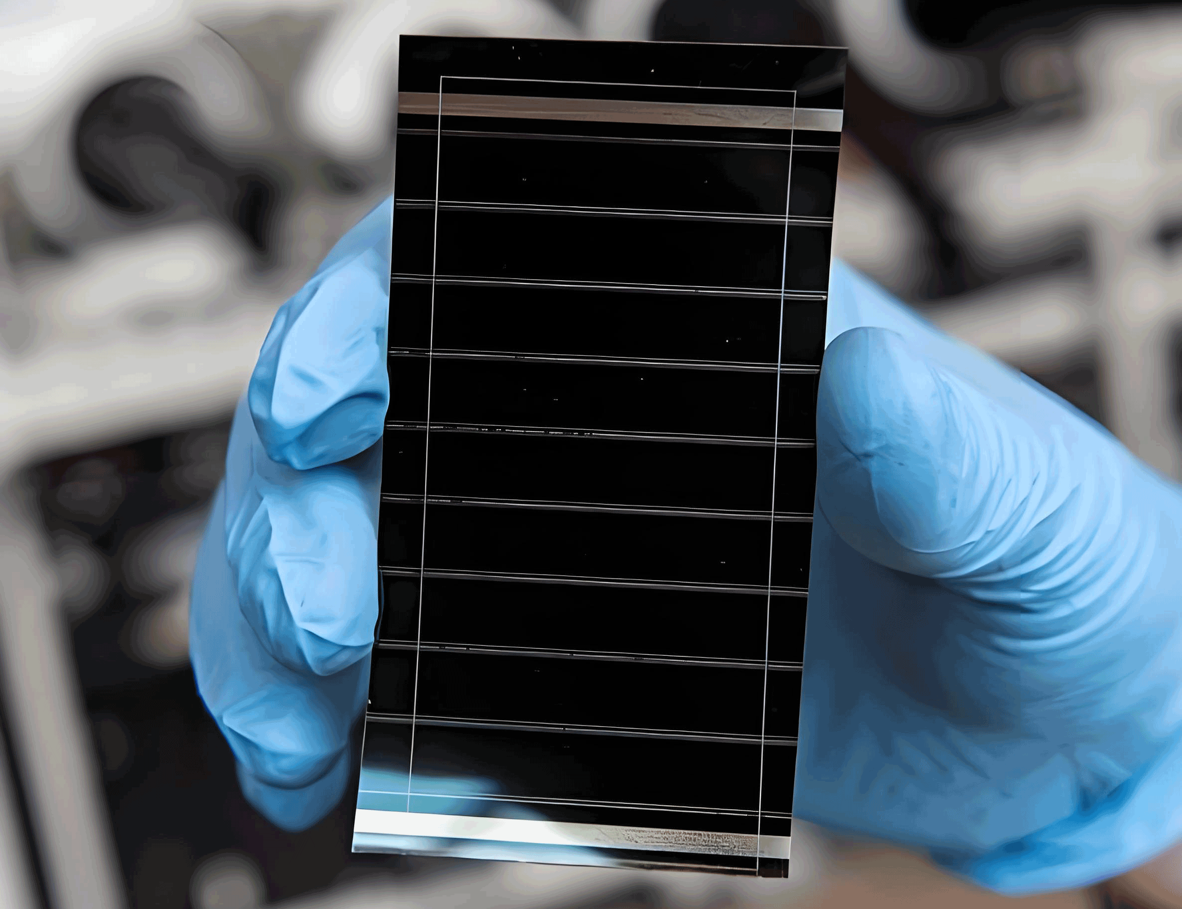
To fabricate the perovskite solar cells, we employed a standard inverted structure: FTO/HTL/MAPbI3/PCBM/BCP/Ag, where the hole transport layer (HTL) is either pristine NiO or K+-doped NiO. The NiO precursor solution was prepared by dissolving nickel acetate tetrahydrate and monoethanolamine in ethanol, with potassium acetate added at varying molar ratios (1% to 7%) for doping. The perovskite layer was formed by spin-coating a MAPbI3 precursor solution, followed by thermal annealing. The electronic transport layers and electrodes were deposited sequentially to complete the perovskite solar cell devices. Characterization techniques included X-ray photoelectron spectroscopy (XPS), grazing-incidence X-ray diffraction (GIXRD), scanning electron microscopy (SEM), space-charge-limited current (SCLC) measurements, and photoluminescence spectroscopy (steady-state and time-resolved) to evaluate the structural, electrical, and optical properties.
The photovoltaic performance of the perovskite solar cells was assessed through current density-voltage (J-V) measurements under simulated sunlight. We observed that K+ doping significantly influenced the short-circuit current density (JSC) and fill factor (FF), while the open-circuit voltage (VOC) remained relatively stable. The optimal doping concentration was found to be 3%, leading to a notable improvement in power conversion efficiency (PCE). The table below summarizes the average photovoltaic parameters for perovskite solar cells with different K+ doping levels:
| K+ Doping (mol%) | JSC (mA/cm2) | VOC (V) | FF | PCE (%) |
|---|---|---|---|---|
| 0 | 19.47 | 1.00 | 0.73 | 14.30 |
| 1 | 20.15 | 1.00 | 0.77 | 15.10 |
| 3 | 20.39 | 1.01 | 0.79 | 16.10 |
| 5 | 19.73 | 1.00 | 0.76 | 14.90 |
| 7 | 19.13 | 1.00 | 0.72 | 13.80 |
The enhancement in JSC and FF can be attributed to improved charge transport and collection in the perovskite solar cells. To elucidate the underlying mechanisms, we examined the electrical properties of NiO films. The electrical conductivity (σ) and hole mobility (μh) are critical parameters for hole transport layers in perovskite solar cells. The conductivity can be expressed as:
$$ \sigma = n e \mu_h $$
where n is the charge carrier density, e is the elementary charge, and μh is the hole mobility. For NiO, the presence of Ni3+ ions, which act as acceptors, increases the hole concentration. We performed dark I-V measurements and SCLC analysis to determine the hole mobility. The SCLC method involves fitting the J-V characteristics in the trap-free region using the Mott-Gurney law:
$$ J = \frac{9}{8} \epsilon_r \epsilon_0 \mu_h \frac{V^2}{L^3} $$
where J is the current density, εr is the relative permittivity, ε0 is the vacuum permittivity, μh is the hole mobility, V is the applied voltage, and L is the film thickness. The results indicated that K+ doping at 3% increased the hole mobility from 1.69 × 10⁻³ cm²/(V·s) for pristine NiO to 6.02 × 10⁻³ cm²/(V·s) for doped NiO. This enhancement directly contributes to the improved JSC in perovskite solar cells.
XPS analysis revealed that K+ doping alters the chemical state of NiO. The Ni 2p spectra showed peaks corresponding to Ni2+ and Ni3+ ions, and the ratio of Ni3+/Ni2+ increased with doping concentration up to 3%, as summarized in the table below:
| K+ Doping (mol%) | Ni3+/Ni2+ Ratio |
|---|---|
| 0 | 2.70 |
| 1 | 3.10 |
| 3 | 3.39 |
| 5 | 2.90 |
| 7 | 2.46 |
The increase in Ni3+ content enhances the p-type character of NiO, facilitating hole transport in perovskite solar cells. Additionally, O 1s spectra indicated the presence of NiO(OH) species in K+-doped samples, which may promote hole injection at the interface due to dipole effects.
Structural characterization via GIXRD showed that K+ doping influences the crystallinity of NiO films. The diffraction peaks corresponding to (111), (200), and (220) planes of NiO were observed, but the intensity decreased with doping, suggesting reduced crystallinity and increased defect density. This aligns with the formation of nickel vacancies, which contribute to higher electrical conductivity. The optical transmittance of NiO films remained high (>80%) across visible wavelengths, indicating that the improvement in perovskite solar cell performance is primarily due to electrical rather than optical effects.
The interfacial properties between NiO and the perovskite layer are crucial for charge collection in perovskite solar cells. SEM images revealed that the average grain size of MAPbI3 films deposited on K+-doped NiO (218 nm) was larger than on pristine NiO (189 nm), implying that K+ ions may act as nucleation sites, promoting perovskite crystallization. However, absorbance and XRD measurements showed minimal changes in the perovskite film itself, confirming that the performance gains stem from interfacial and transport improvements.
Photoluminescence spectroscopy provided insights into the charge separation dynamics. Steady-state photoluminescence (SSPL) spectra exhibited stronger quenching for perovskite films on K+-doped NiO, indicating efficient hole extraction. Time-resolved photoluminescence (TRPL) decay curves were fitted with a bi-exponential model to extract the average carrier lifetime (τavg). The lifetimes decreased from 121 ns for glass/MAPbI3 to 16 ns for NiO/MAPbI3 and further to 6 ns for K+-doped NiO/MAPbI3, demonstrating faster charge transfer and reduced non-radiative recombination at the interface. This enhancement is critical for achieving high JSC and FF in perovskite solar cells.
To further quantify the benefits of K+ doping, we analyzed the energy level alignment using ultraviolet photoelectron spectroscopy (UPS). The valence band maximum (VBM) of NiO shifted from -5.12 eV to -5.20 eV upon K+ doping, reducing the energy barrier for hole injection from the perovskite (VBM ≈ -5.40 eV) to NiO. The improved energy level matching facilitates efficient charge collection in perovskite solar cells. The table below compares the energy levels:
| Material | VBM (eV) | CBM (eV) |
|---|---|---|
| Pristine NiO | -5.12 | -1.43 |
| K+-doped NiO | -5.20 | -1.52 |
| MAPbI3 | -5.40 | -3.90 |
The stability of perovskite solar cells with K+-doped NiO was evaluated through maximum power point tracking. The devices maintained constant current and efficiency over 100 seconds, indicating robust operational stability. This is advantageous for the long-term performance of perovskite solar cells in practical applications.
In conclusion, we have demonstrated that K+ doping in NiO significantly enhances the charge collection capability in inverted perovskite solar cells. The optimal doping concentration of 3% improves the electrical conductivity and hole mobility of NiO by increasing the Ni3+/Ni2+ ratio. Additionally, K+ doping promotes better interfacial contact with the perovskite layer, leading to efficient charge separation and reduced recombination. These improvements result in higher JSC and FF, boosting the overall efficiency of perovskite solar cells. Our findings provide a simple and effective strategy for developing high-performance hole transport layers in inverted perovskite solar cells, contributing to the advancement of stable and efficient photovoltaic devices.
The continued optimization of charge transport layers is essential for pushing the boundaries of perovskite solar cell technology. Future work could explore combinatorial doping strategies or interface engineering to further enhance the performance and stability of perovskite solar cells. The insights gained from this study underscore the importance of material modifications in achieving superior photovoltaic outcomes for perovskite solar cells.