
In recent years, the global energy crisis has highlighted the urgent need for sustainable and clean energy sources. Photovoltaic technology, as a key player in the renewable energy sector, has attracted significant attention due to its potential to achieve carbon neutrality goals. Among various photovoltaic devices, perovskite solar cells have emerged as a promising candidate owing to their low cost and high power conversion efficiency. Since the initial report by Kojima et al. in 2009, where perovskite materials were first applied in solar cells, the efficiency of single-junction perovskite solar cells has skyrocketed from 3.8% to over 26%, showcasing their immense potential for commercial applications. The structure of perovskite solar cells can be categorized into formal (n-i-p) and inverted (p-i-n) configurations based on the position of charge transport layers and electrodes. Inverted perovskite solar cells often employ organic materials like PEDOT:PSS, PTAA, and PCBM as charge transport layers, which offer advantages such as flexibility and low-temperature processability, making them suitable for roll-to-roll manufacturing. However, the morphology of these layers, particularly the electron transport layer (ETL), plays a critical role in determining device performance. A smooth and uniform ETL can reduce internal resistance and enhance charge transport, thereby improving overall efficiency. In this study, we explore the use of a high boiling point solvent, 1,8-octanedithiol (ODT), to control the morphology of the PCBM ETL in inverted perovskite solar cells. We investigate its impact on film morphology, optical properties, electrical conductivity, and device performance through various characterization techniques.
The morphology of organic layers in perovskite solar cells is crucial for achieving high performance. Common methods for controlling morphology include mixed solvents, solvent additives, and solvent annealing, which leverage the solubility and volatility of solvents to reorganize organic molecules during film formation. In this work, we focus on adding ODT, a high boiling point solvent (269.5°C), to chlorobenzene (CB) used for dissolving PCBM. This approach aims to slow down the solvent evaporation rate during spin-coating and annealing, allowing for a more controlled solidification process and resulting in a smoother PCBM film. We hypothesize that this improved morphology will enhance electron extraction and transport, leading to better photovoltaic performance. To test this, we fabricated inverted perovskite solar cells with the structure: glass/ITO/PEDOT:PSS/perovskite/PCBM/BCP/Ag. The perovskite layer was formed by spin-coating a precursor solution of methylammonium iodide and lead iodide in DMF, followed by antisolvent treatment and annealing. The PCBM layer was deposited from solutions in pure CB or CB with varying amounts of ODT (2%, 3%, 4%). We then characterized the films using atomic force microscopy (AFM), steady-state photoluminescence (PL) spectroscopy, UV-visible absorption spectroscopy, conductivity measurements, current density-voltage (J-V) curves, and incident photon-to-electron conversion efficiency (IPCE) spectra.
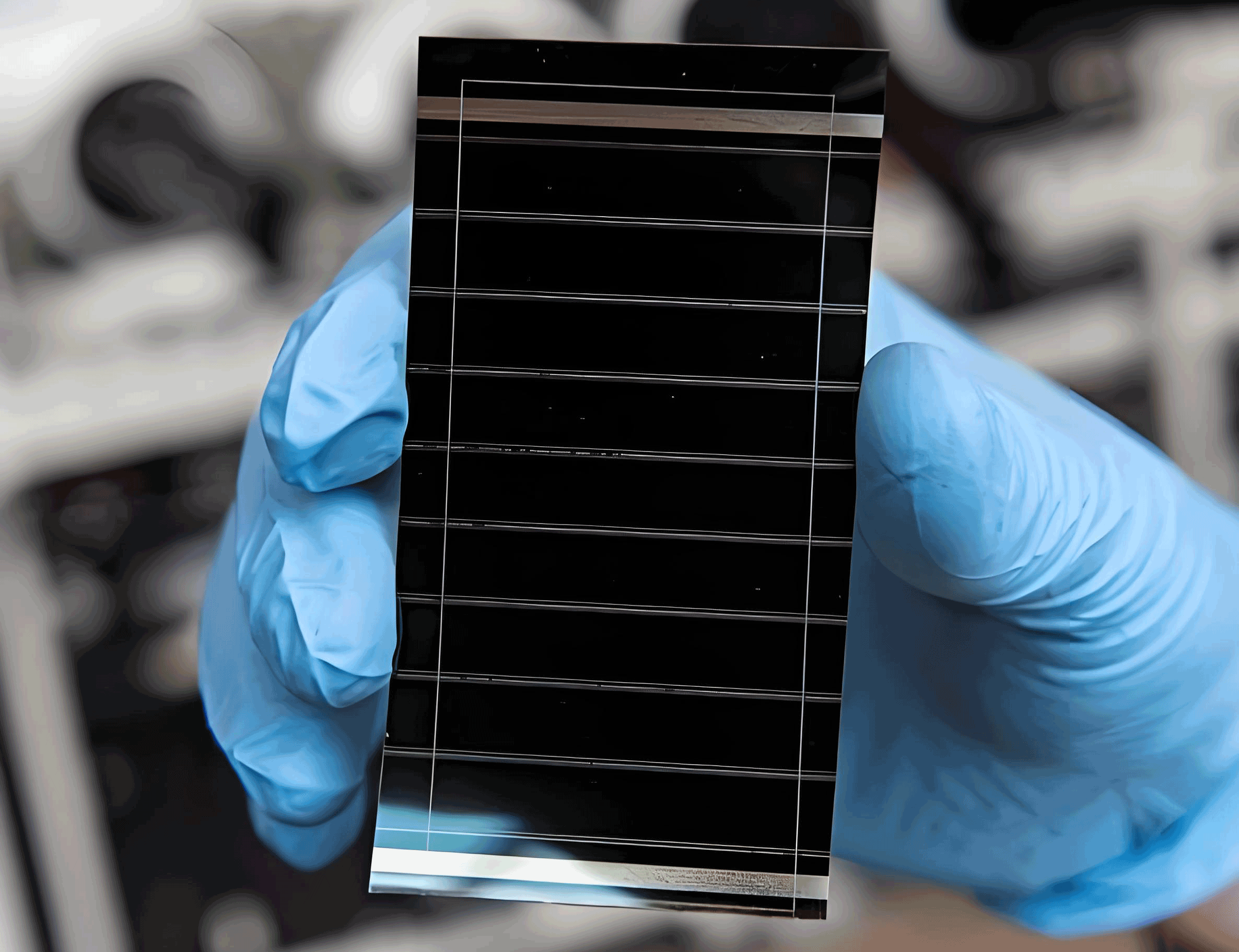
The structure of the perovskite solar cell is depicted in the figure above, showing a typical layered configuration with ITO as the anode, PEDOT:PSS as the hole transport layer (HTL), perovskite as the active layer, PCBM as the ETL, BCP as the hole-blocking layer, and Ag as the cathode. Under illumination, photons are absorbed by the perovskite layer, generating excitons that dissociate at the interfaces with charge transport layers. Electrons are then collected by the cathode via the PCBM layer, while holes are transported to the anode through the PEDOT:PSS layer. The cross-sectional SEM image reveals well-defined layers with thicknesses of approximately 350 nm for the perovskite and 70 nm for the PCBM, consistent with reported values for inverted perovskite solar cells. This structure ensures efficient charge separation and collection, but its performance is highly dependent on the quality of each layer, especially the ETL.
To evaluate the effect of ODT addition on PCBM morphology, we performed AFM analysis on films spin-coated from pure CB and CB with 3% ODT. The AFM images and corresponding height profiles are summarized in Table 1, which compares the root mean square (RMS) roughness and peak-to-valley differences. The PCBM film from pure CB exhibited an RMS roughness of 7.5 nm with significant height variations (peak-to-valley difference of ~20 nm), indicating a rough and inhomogeneous surface. In contrast, the film with 3% ODT showed a much smoother morphology, with an RMS roughness of 3.2 nm and a reduced peak-to-valley difference of ~8 nm. This improvement can be attributed to the slower evaporation rate of ODT, which allows PCBM molecules to reorganize more effectively during film formation. The schematic diagram in Table 1 illustrates the film formation process: in pure CB, rapid solvent evaporation leads to quick solidification and rough morphology, whereas ODT addition prolongs the drying time, enabling the formation of a uniform film. This enhanced morphology is expected to facilitate better contact with adjacent layers and reduce interfacial defects, which are critical for efficient charge transport in perovskite solar cells.
| Solvent System | RMS Roughness (nm) | Peak-to-Valley Difference (nm) | Morphology Description |
|---|---|---|---|
| Pure CB | 7.5 | 20 | Rough and inhomogeneous |
| CB + 3% ODT | 3.2 | 8 | Smooth and uniform |
Further insights into the impact of ODT on charge extraction were obtained from steady-state PL spectroscopy. We measured the PL spectra of perovskite layers alone and in combination with PCBM layers deposited from different solvents. The results, normalized to the perovskite peak at 776 nm, are presented in Table 2. The perovskite layer showed strong PL emission, which was significantly quenched when covered with a PCBM layer from pure CB, indicating efficient electron extraction by PCBM. However, when the PCBM layer was deposited from CB with 3% ODT, the PL quenching was even more pronounced, suggesting enhanced electron extraction efficiency. This improvement aligns with the smoother morphology, as a uniform PCBM layer provides better interfacial contact and reduces recombination losses. The PL quenching efficiency can be quantified using the formula: $$ ext{Quenching Efficiency} = \frac{I_0 – I}{I_0} imes 100\% $$ where \( I_0 \) is the PL intensity of the perovskite alone and \( I \) is the intensity with PCBM. For the ODT-modified PCBM, the quenching efficiency increased, underscoring its superior charge extraction capability in perovskite solar cells.
| Sample | PL Intensity at 776 nm (a.u.) | Quenching Efficiency (%) |
|---|---|---|
| Perovskite alone | 100 | 0 |
| Perovskite + PCBM (pure CB) | 40 | 60 |
| Perovskite + PCBM (CB + 3% ODT) | 25 | 75 |
UV-visible absorption spectroscopy was employed to study the optical properties of PCBM films. The absorption spectra, shown in Table 3, reveal differences between films from pure CB and CB with 3% ODT. The ODT-modified film exhibited reduced absorption in the 450–600 nm range but enhanced absorption in the 300–380 nm region. This spectral shift suggests a decrease in PCBM aggregation, as ODT promotes molecular dispersion due to its better solubility. The absorption coefficient \( \alpha \) can be calculated using the Beer-Lambert law: $$ A = \alpha c l $$ where \( A \) is absorbance, \( c \) is concentration, and \( l \) is path length. The changes in absorption indicate that ODT alters the packing of PCBM molecules, leading to a more disordered and less aggregated structure, which is consistent with the observed smooth morphology. This reduced aggregation may facilitate better charge transport by minimizing trap states and improving interfacial properties in perovskite solar cells.
| Solvent System | Absorption at 450–600 nm (a.u.) | Absorption at 300–380 nm (a.u.) | Interpretation |
|---|---|---|---|
| Pure CB | High | Low | Aggregated PCBM |
| CB + 3% ODT | Low | High | Dispersed PCBM |
Electrical conductivity measurements further support the benefits of ODT addition. We determined the conductivity \( \sigma \) of PCBM films using the formula: $$ \sigma = \frac{1}{\rho} = \frac{I l}{V A} $$ where \( \rho \) is resistivity, \( I \) is current, \( V \) is voltage, \( l \) is film thickness, and \( A \) is cross-sectional area. The results, averaged over multiple devices, are summarized in Table 4. The PCBM film from pure CB had a conductivity of \( 3.6 imes 10^{-6} ext{S} \cdot ext{cm}^{-1} \), while the film with 3% ODT showed a higher conductivity of \( 4.5 imes 10^{-6} ext{S} \cdot ext{cm}^{-1} \). This increase can be attributed to the smoother morphology, which reduces interfacial resistance and enhances electron mobility. The improved conductivity is crucial for minimizing series resistance in perovskite solar cells, thereby boosting fill factor and overall efficiency.
| Solvent System | Conductivity (S·cm⁻¹) | Relative Improvement |
|---|---|---|
| Pure CB | 3.6 × 10⁻⁶ | Baseline |
| CB + 3% ODT | 4.5 × 10⁻⁶ | 25% |
To assess the overall impact on device performance, we fabricated perovskite solar cells with PCBM layers from different solvent systems and measured their J-V characteristics under AM 1.5 illumination. The key parameters—open-circuit voltage (\( V_{ ext{oc}} \)), short-circuit current density (\( J_{ ext{sc}} \)), fill factor (FF), and power conversion efficiency (PCE)—are compiled in Table 5 for devices with ODT concentrations of 0%, 2%, 3%, and 4%. The average PCE increased from \( 12.5 \pm 0.3\% \) for pure CB to \( 15.1 \pm 0.3\% \) for 3% ODT, with corresponding improvements in \( V_{ ext{oc}} \) (from 0.96 V to 1.01 V), \( J_{ ext{sc}} \) (from 19.2 mA·cm⁻² to 20.8 mA·cm⁻²), and FF (from 67.8% to 71.7%). The highest PCE achieved was 15.5% with 3% ODT, demonstrating the optimal concentration for morphology control. The enhancement in \( J_{ ext{sc}} \) can be linked to better charge extraction, as evidenced by PL quenching, while the higher \( V_{ ext{oc}} \) and FF result from reduced recombination and lower series resistance. The PCE can be expressed as: $$ ext{PCE} = \frac{V_{ ext{oc}} imes J_{ ext{sc}} imes ext{FF}}{P_{ ext{in}}} imes 100\% $$ where \( P_{ ext{in}} \) is incident power density (100 mW·cm⁻²). The data clearly show that ODT addition positively influences all parameters, leading to superior perovskite solar cell performance.
| ODT Concentration | \( V_{ ext{oc}} \) (V) | \( J_{ ext{sc}} \) (mA·cm⁻²) | FF (%) | Average PCE (%) | Best PCE (%) |
|---|---|---|---|---|---|
| 0% (Pure CB) | 0.96 ± 0.01 | 19.2 ± 0.3 | 67.8 ± 1.3 | 12.5 ± 0.3 | 12.8 |
| 2% | 0.98 ± 0.01 | 20.5 ± 0.2 | 69.3 ± 1.2 | 13.9 ± 0.2 | 14.3 |
| 3% | 1.01 ± 0.01 | 20.8 ± 0.3 | 71.7 ± 1.3 | 15.1 ± 0.3 | 15.5 |
| 4% | 0.99 ± 0.01 | 20.2 ± 0.3 | 69.2 ± 1.2 | 13.8 ± 0.2 | 14.1 |
IPCE spectra were recorded to validate the \( J_{ ext{sc}} \) values from J-V measurements. The integrated current densities from IPCE curves were 18.8 mA·cm⁻² for pure CB and 20.5 mA·cm⁻² for 3% ODT, which are within 2.5% of the J-V results, confirming the consistency of our data. The IPCE spectrum for the ODT-modified device showed higher values across the visible range, particularly in regions where the perovskite absorbs strongly, indicating improved charge collection efficiency. This aligns with the enhanced morphology and charge transport properties. The IPCE at a specific wavelength \( \lambda \) is given by: $$ ext{IPCE}(\lambda) = \frac{1240 imes J_{ ext{sc}}(\lambda)}{\lambda imes P_{ ext{in}}(\lambda)} imes 100\% $$ where \( J_{ ext{sc}}(\lambda) \) is the short-circuit current density at wavelength \( \lambda \), and \( P_{ ext{in}}(\lambda) \) is the incident power density. The higher IPCE for ODT-based devices underscores the role of morphology in optimizing light harvesting and charge collection in perovskite solar cells.
In conclusion, our study demonstrates that adding a small amount of high boiling point solvent ODT to the PCBM solution effectively controls the morphology of the electron transport layer in perovskite solar cells. The smoother and more uniform PCBM film reduces surface roughness, enhances charge extraction, and improves electrical conductivity. These changes lead to significant improvements in photovoltaic parameters, including \( V_{ ext{oc}} \), \( J_{ ext{sc}} \), FF, and PCE, with an optimal ODT concentration of 3%. This simple and efficient method highlights the importance of solvent engineering in optimizing the performance of perovskite solar cells. Future work could explore other high boiling point solvents or combinations to further enhance stability and efficiency, paving the way for commercial applications of perovskite solar cells.
The mechanisms behind the morphology control can be further elucidated using theoretical models. For instance, the solvent evaporation process can be described by the diffusion equation: $$ \frac{\partial C}{\partial t} = D abla^2 C $$ where \( C \) is solvent concentration, \( t \) is time, and \( D \) is diffusion coefficient. With ODT, the higher boiling point reduces the evaporation rate, allowing for more homogeneous distribution of PCBM molecules. Additionally, the interaction between ODT and PCBM can be analyzed using solubility parameters, where the Hansen solubility parameters \( \delta_d \), \( \delta_p \), and \( \delta_h \) for dispersion, polarity, and hydrogen bonding, respectively, influence the mixing behavior. The distance in Hansen space \( R_a \) between PCBM and solvent can be calculated as: $$ R_a = \sqrt{4(\delta_{d1} – \delta_{d2})^2 + (\delta_{p1} – \delta_{p2})^2 + (\delta_{h1} – \delta_{h2})^2} $$ where smaller \( R_a \) values indicate better solubility. ODT likely has a smaller \( R_a \) with PCBM compared to CB alone, promoting better dispersion and film formation.
Moreover, the charge transport in PCBM can be modeled using the Gaussian disorder model (GDM), where the charge mobility \( \mu \) depends on the energetic disorder \( \sigma \) and positional disorder \( \Sigma \): $$ \mu = \mu_0 \exp\left[ -\left( \frac{2\sigma}{3kT} \right)^2 \right] \exp\left[ C (\sigma^2 – \Sigma^2) \sqrt{\frac{E}{a}} \right] $$ where \( \mu_0 \) is prefactor mobility, \( k \) is Boltzmann constant, \( T \) is temperature, \( E \) is electric field, \( a \) is lattice constant, and \( C \) is a constant. The smoother morphology with ODT reduces \( \sigma \) and \( \Sigma \), leading to higher mobility and conductivity. This theoretical framework supports our experimental findings and provides insights for future optimization of perovskite solar cells.
In summary, the integration of high boiling point solvents like ODT into the fabrication process of perovskite solar cells offers a straightforward yet powerful strategy to enhance device performance. By improving the morphology of the PCBM electron transport layer, we achieve better charge transport, reduced recombination, and higher efficiency. This approach not only advances the understanding of morphology-property relationships but also contributes to the development of high-performance and scalable perovskite solar cells for sustainable energy solutions.