
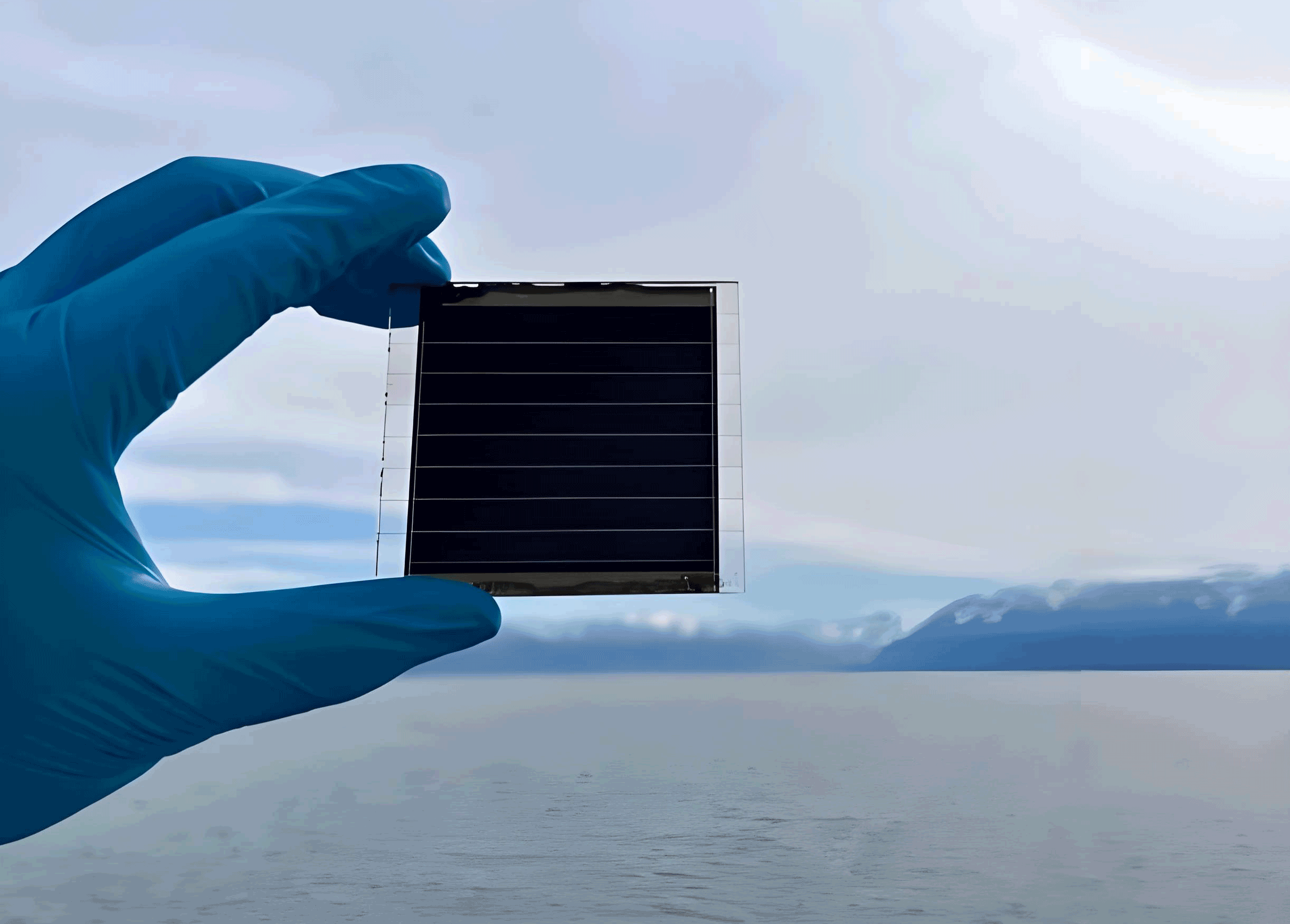
In recent years, perovskite solar cells have emerged as a promising third-generation photovoltaic technology due to their rapidly improving power conversion efficiencies, solution-based fabrication processes, and low raw material costs. Among various architectures, inverted (p-i-n) perovskite solar cells have garnered significant attention owing to their superior stability and high efficiency. The current efficiency record for small-area rigid inverted perovskite solar cells exceeds 26%, highlighting their immense potential. However, the presence of interfacial defects between the perovskite layer and charge transport layers—specifically, the upper interface with the electron transport layer and the lower interface with the hole transport layer—remains a critical factor limiting further improvements in power conversion efficiency. These defects induce non-radiative recombination, impairing charge carrier extraction and overall device performance.
To address these challenges, various strategies have been employed, including additive engineering, composition engineering, and interface passivation. Organic amine salts, in particular, have been widely utilized to passivate surface defects in perovskite films. For instance, previous studies have demonstrated that alkylamine salts with different chain lengths can effectively reduce defect densities. Similarly, two-dimensional perovskite layers and diamine molecules have been used to modify perovskite surfaces, leading to significant efficiency enhancements in both single-junction and tandem solar cells. In this context, 1,3-diaminopropane dihydroiodide (PDADI) has shown promise as a passivation agent that does not form new perovskite phases upon annealing but directly passivates surface defects, resulting in reduced non-radiative recombination and improved charge carrier transport.
This work presents a comprehensive study on the application of a PDADI dual-modification strategy to fabricate high-performance inverted perovskite solar cells. The approach involves modifying both the hole transport layer (NiOx) and the perovskite surface with PDADI to enhance film quality, reduce interfacial defects, and suppress non-radiative recombination. Through detailed morphological, structural, and optoelectronic characterizations, we demonstrate that this dual-modification strategy significantly improves the power conversion efficiency and stability of inverted perovskite solar cells.
Experimental Section
Materials and Reagents
Lead iodide (PbI2), cesium iodide (CsI), formamidinium iodide (FAI), methylammonium chloride (MACl), bathocuproine (BCP), and 1,3-diaminopropane dihydroiodide (PDADI) were procured from commercial suppliers. Phenyl-C61-butyric acid methyl ester (PCBM) was obtained from a specialized materials company. N,N-Dimethylformamide (DMF), dimethyl sulfoxide (DMSO), chlorobenzene, and anhydrous ethanol were purchased from chemical reagent distributors. Fluorine-doped tin oxide (FTO) glass substrates were acquired from a solar technology company. Silver evaporation pellets and nickel oxide (NiOx) evaporation materials were sourced from advanced materials suppliers.
Device Fabrication
FTO glass substrates were sequentially cleaned in deionized water, acetone, and isopropanol using ultrasonic baths for 30 minutes each, followed by drying under nitrogen flow. The cleaned substrates were treated with UV ozone for 15 minutes to enhance surface wettability. A 23 nm thick NiOx layer was deposited via electron beam evaporation under a vacuum pressure below 1.3 × 10⁻³ Pa, resulting in glass/FTO/NiOx substrates.
For the single-modification approach, a 0.25 mg/mL PDADI solution in ethanol was spin-coated onto the NiOx surface at 3000 rpm for 30 seconds (acceleration: 3000 rpm/s) and annealed at 100°C for 10 minutes. The perovskite precursor solution was prepared by dissolving 613 mg PbI2, 196 mg FAI, 26 mg CsI, and 14 mg MACl in a mixture of 800 μL DMF and 200 μL DMSO, corresponding to a Cs0.08FA0.92PbI3 composition. The solution was stirred for 3 hours and filtered through a 0.45 μm syringe filter. The perovskite layer was deposited via a two-step spin-coating process: 1000 rpm for 5 seconds (acceleration: 500 rpm/s) followed by 3000 rpm for 30 seconds (acceleration: 3000 rpm/s). Chlorobenzene (200 μL) was dripped as an anti-solvent 15 seconds before the end of the second step. The film was annealed at 110°C for 20 minutes and cooled to room temperature.
For the dual-modification approach, a 0.5 mg/mL PDADI solution in ethanol was spin-coated onto the perovskite surface at 3000 rpm for 30 seconds and annealed at 100°C for 10 minutes. Subsequently, PCBM (20 mg/mL in chlorobenzene) and BCP (saturated solution in isopropanol) were spin-coated at 3000 rpm for 30 seconds and 5000 rpm for 35 seconds, respectively. Finally, a 150 nm thick silver electrode was deposited via thermal evaporation.
Characterization Techniques
X-ray photoelectron spectroscopy (XPS) and ultraviolet photoelectron spectroscopy (UPS) were performed using a Thermo ESCALAB 250Xi system. Steady-state photoluminescence (PL) and time-resolved photoluminescence (TRPL) spectra were recorded at room temperature using an FLS920 spectrometer. Mott-Schottky analysis was conducted with a Zahner Zennium IM6e electrochemical workstation. Space-charge-limited current (SCLC) measurements were carried out in the dark using a Keithley 2450 source measure unit. Field-emission scanning electron microscopy (SEM) images were acquired with a Hitachi SU8020 microscope. X-ray diffraction (XRD) patterns were obtained using a Cu Kα1 radiation source (λ = 1.541 Å). Atomic force microscopy (AFM) measurements were performed with a Bruker Nanowizard 4XP system. Current density-voltage (J-V) characteristics were measured using a Keysight B2901A source measure unit.
Results and Discussion
Morphological and Structural Properties
The impact of PDADI modification on perovskite film morphology was investigated using SEM and AFM. Unmodified perovskite films exhibited small grains with numerous boundaries, voids, and pinholes (Figure 1a). Single-modification (PDADI on NiOx) resulted in larger grains and reduced surface impurities, but grain boundaries remained visible (Figure 1b). Dual-modification (PDADI on both NiOx and perovskite) yielded densely packed grains with minimized boundaries and enhanced surface coverage (Figure 1c). Grain size distribution analysis revealed that unmodified films had predominant sizes of 250–350 nm, single-modified films 350–450 nm, and dual-modified films 450–650 nm (Figure 1d). AFM measurements confirmed reduced surface roughness: unmodified films had a roughness (Ra) of 17.3 nm, single-modified 15.5 nm, and dual-modified 15.2 nm (Figure 2). This improvement is attributed to PDADI filling grain boundaries and promoting large-grained growth.
Water contact angle measurements demonstrated that PDADI modification enhanced the wettability of NiOx surfaces, reducing the contact angle from 40.85° to 25.92° (Figure 3a,b). Conversely, perovskite surfaces became more hydrophobic after modification, with contact angles increasing from 45.79° (unmodified) to 47.56° (single-modified) and 51.08° (dual-modified) (Figure 3c–e). This hydrophobicity is beneficial for moisture resistance and device stability.
XRD analysis showed intensified (100) diffraction peaks and reduced full width at half maximum (FWHM) values for modified films, indicating improved crystallinity and larger grain sizes (Figure 4). The FWHM decreased from 0.236° (unmodified) to 0.139° (dual-modified), consistent with SEM observations.
Defect Passivation and Optoelectronic Properties
Steady-state PL spectra exhibited quenched emission for modified films, suggesting enhanced charge extraction (Figure 5a). TRPL decay curves were fitted using a bi-exponential model:
$$f(t) = A_1 \exp\left(-\frac{t}{\tau_1}\right) + A_2 \exp\left(-\frac{t}{\tau_2}\right) + B,$$
where τ1 and τ2 represent fast and slow decay constants, respectively, and A1, A2, and B are fitting parameters. The average carrier lifetime (τave) was calculated as:
$$\tau_{\text{ave}} = \frac{A_1 \tau_1^2 + A_2 \tau_2^2}{A_1 \tau_1 + A_2 \tau_2}.$$
Unmodified films had τave = 311.27 ns, single-modified 295.77 ns, and dual-modified 220.21 ns (Table 1). The reduced lifetime indicates suppressed non-radiative recombination and efficient charge extraction.
SCLC measurements on hole-only devices revealed lower trap-filled limit voltages (VTFL) for modified films: 0.64 V (unmodified), 0.43 V (single-modified), and 0.31 V (dual-modified) (Figure 6). The defect density (Nt) was calculated using:
$$N_t = \frac{2 \epsilon \epsilon_0 V_{\text{TFL}}}{e L^2},$$
where ε = 46.9 is the relative permittivity, ε0 is the vacuum permittivity, e is the elementary charge, and L ≈ 500 nm is the film thickness. Nt values were 1.32 × 1016 cm−3 (unmodified), 8.92 × 1015 cm−3 (single-modified), and 6.43 × 1015 cm−3 (dual-modified), confirming effective defect passivation.
Energy Level Alignment
UPS analysis showed that PDADI modification shifted the valence band maximum (VBM) of NiOx from 5.60 eV to 5.83 eV, aligning better with the perovskite VBM (5.62 eV for unmodified, 5.82 eV for modified) (Figure 7). The Fermi level positions indicated a transition from p-type to more n-type characteristics, facilitating electron extraction. The built-in potential (Vbi) derived from Mott-Schottky plots increased from 0.92 V (unmodified) to 0.93 V (single-modified) and 0.96 V (dual-modified) (Figure 9), promoting charge separation.
Photovoltaic Performance
J-V measurements under AM 1.5G illumination demonstrated improved performance for modified devices (Figure 8a, Table 2). The hysteresis index decreased from 11% (unmodified) to 6% (single-modified) and 3% (dual-modified). Dual-modified devices achieved a champion efficiency of 23.19% (VOC = 1.09 V, JSC = 25.36 mA/cm2, FF = 84.15%), compared to 21.34% for unmodified and 22.27% for single-modified devices. The ideal factor (n) derived from VOC-light intensity plots decreased from 1.609 (unmodified) to 1.46 (single-modified) and 1.38 (dual-modified), indicating suppressed trap-assisted recombination (Figure 8f). External quantum efficiency (EQE) spectra showed integrated JSC values consistent with J-V measurements (Figure 8g). Stability tests under ambient conditions (25°C, <20% RH) revealed that dual-modified devices retained 96% of initial efficiency after 600 hours, outperforming single-modified (90%) and unmodified (80%) devices (Figure 8h).
Conclusion
This study demonstrates that a PDADI dual-modification strategy effectively enhances the performance and stability of inverted perovskite solar cells. By passivating interfacial defects and improving energy level alignment, this approach reduces non-radiative recombination, enhances charge extraction, and increases the built-in potential. The optimized devices achieve a power conversion efficiency of 23.19% with superior operational stability. These findings provide a robust framework for developing high-efficiency inverted perovskite solar cells through rational interface engineering.
| Sample | τ1 (ns) | A1 | τ2 (ns) | A2 | τave (ns) |
|---|---|---|---|---|---|
| Unmodified | 149.17 | 23.40 | 2089.05 | 1.16 | 311.27 |
| Single-Modified | 228.55 | 14.99 | 1528.54 | 0.82 | 295.77 |
| Dual-Modified | 183.40 | 28.71 | 991.57 | 1.37 | 220.21 |
| Sample | Scan Direction | VOC (V) | JSC (mA/cm2) | FF (%) | PCE (%) |
|---|---|---|---|---|---|
| Unmodified | Forward | 1.02 | 25.04 | 73.02 | 18.80 |
| Reverse | 1.04 | 25.16 | 81.19 | 21.34 | |
| Single-Modified | Forward | 1.05 | 25.19 | 77.99 | 20.81 |
| Reverse | 1.06 | 25.24 | 82.89 | 22.27 | |
| Dual-Modified | Forward | 1.09 | 25.34 | 82.25 | 22.55 |
| Reverse | 1.09 | 25.36 | 84.15 | 23.19 |
The development of efficient and stable perovskite solar cells is crucial for advancing renewable energy technologies. The dual-modification strategy presented here offers a scalable and effective method to optimize interface properties in inverted perovskite solar cells. Future work will focus on extending this approach to large-area modules and tandem configurations to further push the boundaries of photovoltaic performance.