
In recent years, perovskite solar cells have emerged as a leading photovoltaic technology due to their rapid efficiency improvements and versatile tunability. Since their first report in 2009, the power conversion efficiency (PCE) of single-junction perovskite solar cells has surged from 3.8% to 26.95%, rivaling traditional crystalline silicon cells. This progress is largely attributed to the unique properties of perovskite materials, which are represented by the chemical formula ABX3, where A sites include cations like formamidinium (FA+), methylammonium (MA+), and cesium (Cs+); B sites comprise divalent metal cations such as lead (Pb2+) and tin (Sn2+); and X sites are halide anions like iodide (I–), bromide (Br–), and chloride (Cl–). The bandgap of perovskites can be tuned from 1.2 to 2.3 eV through ion substitution, making them ideal for tandem solar cell applications, including perovskite/silicon, perovskite/copper indium gallium selenide, and all-perovskite configurations. Among these, all-perovskite tandem solar cells offer superior flexibility in bandgap matching, combining wide-bandgap top cells with narrow-bandgap bottom cells to achieve broader spectral response and reduced thermal losses. According to the Shockley-Queisser (S-Q) theory, the theoretical efficiency limit for such tandem structures exceeds 45%. Recent laboratory achievements have demonstrated PCEs over 29% for all-perovskite tandem solar cells, leveraging solution-processable techniques for cost-effective fabrication. However, challenges such as ion migration, phase separation in narrow-bandgap perovskites, energy-level mismatches at interlayers, and non-radiative recombination in wide-bandgap top cells hinder further advancements. To address these issues, we propose a dual-absorption-layer perovskite heterojunction (DPHJ) strategy, which involves integrating a type-II staggered heterojunction (p-pCsPbI2Br-CsPbIBr2) into the absorption layer of the top cell in an all-perovskite tandem solar cell. This approach aims to enhance light absorption, promote carrier transport, and suppress non-radiative recombination, ultimately boosting the photovoltaic performance of perovskite solar cells.
The DPHJ strategy is grounded in comprehensive numerical simulations and experimental validations. We employed the Silvaco software and a photovoltaic cell simulation platform to model the performance of perovskite solar cells. The current density-voltage (J-V) characteristics are described by the following equation:
$$J = J_{\text{ph}} – J_0 \left\{ \exp \left[ \frac{q(V + J R_S)}{m k_B T} \right] – 1 \right\} – \frac{V + J R_S}{R_{\text{Sh}}},$$
where \(J_0\) is the reverse saturation dark current density, \(q\) is the elementary charge, \(m\) is the ideality factor, \(k_B\) is the Boltzmann constant, \(R_S\) is the series resistance, \(R_{\text{Sh}}\) is the shunt resistance, \(T\) is the temperature, and \(J_{\text{ph}}\) is the photogenerated current density. The Shockley-Read-Hall (SRH) recombination model is used to account for carrier recombination, trapping, doping, and electric field distributions. The SRH recombination rate is defined as:
$$R_{\text{SRH}} = \frac{np – n_i p_i}{\tau_n p + \tau_p n},$$
where \(n\) and \(p\) are the electron and hole concentrations, \(n_i\) and \(p_i\) are the intrinsic carrier concentrations, and \(\tau_n\) and \(\tau_p\) are the lifetimes of free electrons and holes, respectively. The drift-diffusion equations for electrons and holes are given by:
$$J_n = q D_n \frac{\partial n}{\partial x} + q \mu_n n E, \quad J_p = -q D_p \frac{\partial p}{\partial x} + q \mu_p p E,$$
where \(\mu_n\) and \(\mu_p\) are the electron and hole mobilities, \(D_n\) and \(D_p\) are the diffusion coefficients, and \(E\) is the electric field strength. Under illumination, the continuity equations for electrons and holes in steady state are:
$$\frac{\partial J_n}{\partial x} + q G_n = q R_n, \quad -\frac{\partial J_p}{\partial x} + q G_p = q R_p,$$
where \(G_n\) and \(R_n\) are the generation and recombination rates for electrons, and \(G_p\) and \(R_p\) are for holes. The carrier generation rate \(G(x)\) at position \(x\) is calculated using the transfer matrix method to simulate electromagnetic wave propagation in layered media, accounting for reflection, transmission, and interference phenomena:
$$G(x) = \int_{\lambda_{\text{min}}}^{\lambda_{\text{max}}} \phi(\lambda) \alpha(\lambda) e^{-\alpha(\lambda) x} d\lambda,$$
where \(\phi(\lambda)\) is the photon flux at wavelength \(\lambda\) under AM1.5G standard spectrum, and \(\alpha(\lambda)\) is the absorption coefficient. The short-circuit current density \(J_{\text{SC}}\) is obtained by integrating the absorbed photon flux across all layers:
$$J_{\text{SC}} = q \sum_i \int_{\lambda_{\text{min}}}^{\lambda_{\text{max}}} A_i(\lambda) \phi(\lambda) d\lambda,$$
where \(A_i(\lambda)\) is the light absorption rate of the i-th layer. The PCE of the perovskite solar cell is defined as:
$$\text{PCE} = \text{FF} \cdot J_{\text{SC}} \cdot V_{\text{OC}} / P_{\text{in}}, \quad \text{FF} = \frac{V_{\text{mp}} \cdot J_{\text{mp}}}{V_{\text{OC}} \cdot J_{\text{SC}}},$$
where FF is the fill factor, \(P_{\text{in}}\) is the incident light power, and \(V_{\text{mp}}\) and \(J_{\text{mp}}\) are the voltage and current density at the maximum power point, respectively.
For the DPHJ-based solar cells, we simulated a single-junction structure with glass/ITO/SnO2/CsPbI2Br/CsPbIBr2/spiro-OMeTAD/Au and a tandem structure with glass/ITO/SnO2/CsPbI2Br/CsPbIBr2/spiro-OMeTAD/ITL/PCBM/CsSnI3/NiOx/Au. The material parameters used in the simulations are summarized in Table 1. CsPbI2Br and CsPbIBr2 are direct-bandgap semiconductors with bandgaps of 1.92 eV and 2.11 eV, respectively, while CsSnI3 serves as the narrow-bandgap (1.27 eV) absorber for the bottom cell. SnO2 and spiro-OMeTAD are chosen as the electron and hole transport layers, respectively, and the interlayer (ITL) is defined as an electrode with high contact resistance to ensure proper current flow.
| Parameter | CsPbI2Br | CsPbIBr2 | CsSnI3 | NiOX | PCBM | SnO2 | Spiro-OMeTAD |
|---|---|---|---|---|---|---|---|
| Thickness (nm) | 300 | 100 | 800 | 30 | 30 | 50 | 50 |
| Acceptor concentration (cm–3) | 1 × 10¹⁵ | 1 × 10¹⁵ | 5 × 10¹⁶ | 1 × 10¹⁵ | 0 | 0 | 1 × 10¹⁹ |
| Donor concentration (cm–3) | 0 | 0 | 0 | 0 | 5 × 10¹⁷ | 1 × 10¹⁹ | 0 |
| Bandgap (eV) | 1.92 | 2.11 | 1.27 | 3.50 | 2.00 | 3.49 | 2.60 |
| Conduction band effective density of states (cm–3) | 5.1 × 10¹⁷ | 1 × 10¹⁹ | 1.58 × 10¹⁹ | 2.8 × 10¹⁹ | 1 × 10¹⁹ | 4.36 × 10¹⁸ | 2.5 × 10²⁰ |
| Valence band effective density of states (cm–3) | 1.8 × 10¹⁸ | 1 × 10¹⁹ | 1.47 × 10¹⁸ | 1.8 × 10¹⁹ | 1 × 10¹⁹ | 2.52 × 10¹⁹ | 2.5 × 10²⁰ |
| Electron affinity (eV) | 4.16 | 3.56 | 4.47 | 1.80 | 4.30 | 4.31 | 2.60 |
| Relative dielectric constant | 7.43 | 20.00 | 10.59 | 10.70 | 4.00 | 9.00 | 3.00 |
| Electron mobility (cm2·V–1·s–1) | 1.02 × 10⁵ | 2.3 × 10³ | 4.37 | 12.00 | 1 × 10⁻⁴ | 240.00 | 2 × 10⁻⁴ |
| Hole mobility (cm2·V–1·s–1) | 1.93 × 10⁴ | 3.2 × 10² | 4.37 | 25.00 | 1 × 10⁻² | 25.00 | 2 × 10⁻⁴ |
In single-junction perovskite solar cells, the DPHJ strategy significantly enhances photovoltaic performance. We compared a control device with a single CsPbI2Br absorption layer (300 nm) to DPHJ devices with varying thicknesses of CsPbIBr2 (50–200 nm) atop CsPbI2Br. As the CsPbIBr2 thickness increases, \(J_{\text{SC}}\) rises from 15.97 mA·cm–2 to 16.80 mA·cm–2, attributed to improved light utilization and carrier generation. The open-circuit voltage \(V_{\text{OC}}\) peaks at 1.47 V with a 50 nm CsPbIBr2 layer, compared to 1.35 V for the control, and then gradually decreases with thicker layers. The fill factor follows a similar trend, consistent with experimental reports. Overall, the DPHJ device with 100 nm CsPbIBr2 achieves a maximum PCE of 22.29%, outperforming the control (19.46%). This improvement stems from the type-II band alignment at the CsPbI2Br/CsPbIBr2 interface, which creates a conduction band offset of 0.63 eV and a valence band offset of 0.42 eV. The band bending induces a stronger built-in electric field, enhancing carrier transport and suppressing non-radiative recombination. Specifically, the electric field intensity in the CsPbI2Br layer of the DPHJ device reaches approximately 3.1 V·μm–1, compared to 0.6 V·μm–1 in the control, and peaks at 4.9 V·μm–1 near the heterojunction interface. This facilitates hole extraction while blocking electron entry into CsPbIBr2, reducing recombination. Analysis of carrier concentrations shows that the hole density in the CsPbIBr2 region of the DPHJ device (1011–1015 cm–3) is significantly higher than in the control (108–1011 cm–3), indicating enhanced hole extraction. Consequently, the recombination rate at the interface and within the absorption layer is lower in the DPHJ device, leading to a reduced reverse saturation current density \(J_0\) and increased \(J_{\text{SC}}\). The \(V_{\text{OC}}\) can be semi-quantitatively estimated by:
$$V_{\text{OC}} \approx \frac{k_B T}{q} \ln \left( \frac{J_{\text{SC}}}{J_0} + 1 \right),$$
where the increase in \(J_{\text{SC}}\) and decrease in \(J_0\) synergistically boost \(V_{\text{OC}}\).
For all-perovskite tandem solar cells, we designed a two-terminal (2T) structure with the DPHJ as the top cell and CsSnI3 as the bottom cell. The filtered light through the top cell reduces spectral irradiance below 650 nm, which serves as the incident light for the bottom cell. By optimizing the thickness of the CsSnI3 layer, we achieved current matching between the top and bottom subcells. As shown in Figure 1, the \(J_{\text{SC}}\) of the bottom cell increases with CsSnI3 thickness, saturating at 16.76 mA·cm–2 for an 800 nm layer. The DPHJ-based tandem solar cell exhibits a \(V_{\text{OC}}\) of 2.25 V, \(J_{\text{SC}}\) of 16.76 mA·cm–2, and PCE of 32.47%, surpassing the control tandem device (2.16 V, 15.96 mA·cm–2, 29.56% PCE). The external quantum efficiency (EQE) analysis reveals enhanced response in the 500–580 nm range for the DPHJ top cell, due to the band-edge absorption of CsPbIBr2, contributing to higher photocurrent. The superior performance of the DPHJ tandem perovskite solar cell underscores the effectiveness of the dual-absorption-layer strategy in maximizing light harvesting and minimizing losses.
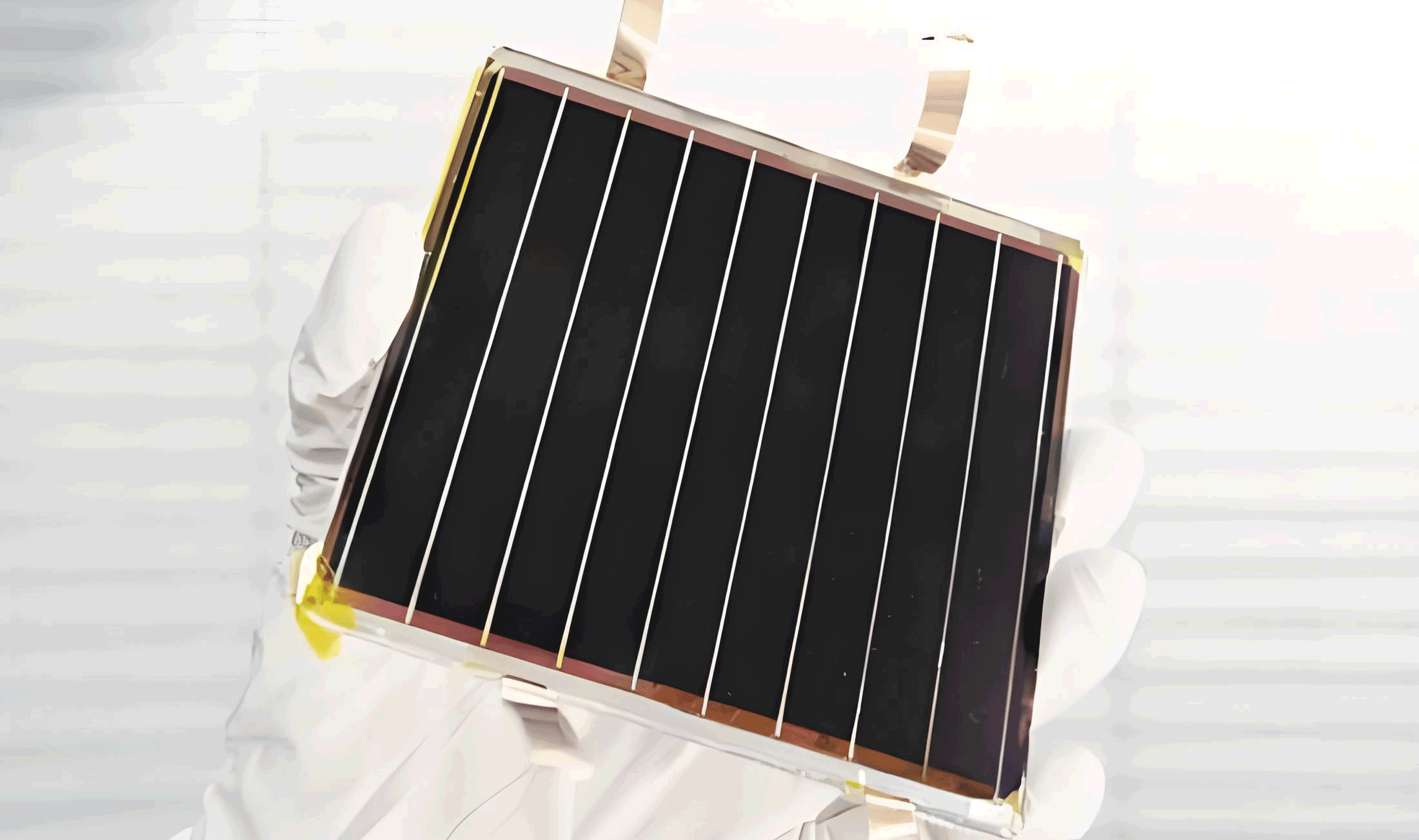
Experimentally, we fabricated single-layer (CsPbI2Br, CsPbIBr2) and dual-layer (DPHJ) films using a two-step spin-coating method. The precursor solutions were prepared by dissolving CsI, PbI2, and PbBr2 in dimethyl sulfoxide (DMSO) and N,N-dimethylformamide (DMF) solvents, followed by annealing at elevated temperatures. The DPHJ film was obtained by sequentially depositing CsPbI2Br and CsPbIBr2 layers, with the latter optimized with acetonitrile (ACN) and ethanol additives. We characterized the films using temperature-dependent photoluminescence (PL) and continuous light-soaking PL measurements. As the temperature increases from 10 K to 350 K, the PL intensity decreases and the full width at half maximum (FWHM) broadens for all films, indicative of thermal quenching and electron-phonon interactions. The PL intensity retention at 350 K relative to 10 K is 3% for CsPbI2Br, 16% for CsPbIBr2, and 11% for DPHJ, demonstrating the superior thermal stability of CsPbIBr2 and its protective role in the DPHJ structure. The temperature-dependent PL data were fitted using a double-exponential Arrhenius equation:
$$I_{\text{PL}}(T) = \frac{I_0}{1 + A e^{-E_1 / k_B T} + B e^{-E_2 / k_B T}},$$
where \(I_0\) is the PL intensity at 0 K, \(A\) and \(B\) are weighting factors, and \(E_1\) and \(E_2\) are the exciton binding energies at low and high temperatures, respectively. The fitting parameters are listed in Table 2. The DPHJ film exhibits higher exciton binding energies (\(E_1 = 8.98\) meV, \(E_2 = 110.7\) meV) compared to CsPbI2Br (\(E_1 = 7.85\) meV, \(E_2 = 101.9\) meV), which helps mitigate non-radiative decay mechanisms such as electron-phonon coupling and defect-assisted recombination. The PL broadening with temperature is described by:
$$\Gamma(T) = \Gamma_0 + \gamma_{\text{ac}} T + \frac{\gamma_{\text{LO}}}{e^{E_{\text{LO}} / k_B T} – 1},$$
where \(\Gamma_0\) is the FWHM at 0 K, \(E_{\text{LO}}\) is the longitudinal optical phonon energy, and \(\gamma_{\text{ac}}\) and \(\gamma_{\text{LO}}\) represent the electron-phonon coupling strengths for acoustic and optical phonons, respectively. The DPHJ film shows reduced electron-phonon coupling strengths (\(\gamma_{\text{ac}} = 1.1 \times 10^{-2}\), \(\gamma_{\text{LO}} = 6.3 \times 10^3\)) relative to CsPbI2Br (\(\gamma_{\text{ac}} = 1.2 \times 10^{-2}\), \(\gamma_{\text{LO}} = 6.9 \times 10^3\)), which suppresses phase segregation under illumination. Light-soaking tests under white LED (100 mW·cm–2) reveal that the CsPbI2Br film undergoes significant peak shifts (red-shift for I-rich phases and blue-shift for Br-rich phases) over 84 hours, indicating phase separation. In contrast, the CsPbIBr2 and DPHJ films exhibit minimal peak shifts and slower PL intensity decay, highlighting their enhanced photostability. The optical bandgaps, determined from Tauc plots using the equation:
$$(\alpha h \nu)^2 \propto (h \nu – E_g),$$
are 1.88 eV for CsPbI2Br, 2.13 eV for CsPbIBr2, and 1.91 eV for DPHJ. The DPHJ film also shows higher absorbance and a shifted PL peak, confirming efficient carrier generation and separation. Long-term stability tests in ambient air (>60% relative humidity) show that CsPbI2Br films degrade within 50 days, while CsPbIBr2 films remain stable, further validating the protective role of the dual-layer structure.
| Sample | \(E_1\) (meV) | \(E_2\) (meV) | \(\gamma_{\text{ac}}\) | \(\gamma_{\text{LO}}\) | \(E_{\text{LO}}\) (meV) |
|---|---|---|---|---|---|
| CsPbI2Br | 7.85 | 101.9 | 1.2 × 10⁻² | 6.9 × 10³ | 156.6 |
| CsPbIBr2 | 9.25 | 85.8 | 1.8 × 10⁻³ | 5.8 × 10³ | 167.7 |
| DPHJ | 8.98 | 110.7 | 1.1 × 10⁻² | 6.3 × 10³ | 162.5 |
To contextualize our findings, we benchmark the performance of DPHJ-based perovskite solar cells against reported values for CsPbI2Br single-junction and all-perovskite tandem devices. Single-junction CsPbI2Br solar cells typically exhibit \(V_{\text{OC}}\) values below 1.4 V, approaching 85% of the theoretical limit (1.61 eV). The DPHJ strategy pushes the \(V_{\text{OC}}\) to 1.46 V in single-junction devices, representing a 0.11 V improvement. In tandem configurations, the top cell’s \(V_{\text{OC}}\) dominates the overall tandem performance (contributing over 65%), and the DPHJ approach elevates the tandem \(V_{\text{OC}}\) to 2.25 V. Our simulated PCE of 32.47% for the DPHJ tandem perovskite solar cell exceeds current experimental records, highlighting the potential of this strategy. Moreover, the DPHJ design offers a universal framework for optimizing absorption layers in multi-junction perovskite solar cells, paving the way for further efficiency gains.
In conclusion, the dual-absorption-layer perovskite heterojunction strategy significantly enhances the photovoltaic performance of all-perovskite tandem solar cells. By incorporating a type-II heterojunction (p-pCsPbI2Br-CsPbIBr2) into the top cell, we achieve improved light absorption, enhanced carrier transport, and suppressed non-radiative recombination. The DPHJ-based tandem solar cell delivers a high \(V_{\text{OC}}\) of 2.25 V, \(J_{\text{SC}}\) of 16.76 mA·cm–2, and PCE of 32.47%, outperforming conventional single-absorption-layer designs. Experimental results confirm that the DPHJ films exhibit higher exciton binding energies, reduced electron-phonon coupling, and superior optical and thermal stability, which are crucial for long-term device operation. This work provides a novel perspective on absorption layer engineering for perovskite solar cells and sets a foundation for developing high-efficiency, stable all-perovskite tandem photovoltaic systems.