
Solar power generation is the most promising renewable energy generation method in the 21st century. Due to its utilization of clean solar energy, it is beneficial for environmental protection, has no movable components, and can be dispersed and flexibly configured. Solar photovoltaic power generation systems are divided into off grid solar photovoltaic power generation systems, grid connected power generation systems, and hybrid systems based on whether they are connected to the power grid. Among them, grid connected solar power generation systems are the development trend of photovoltaic power generation systems, Its composition mainly includes solar cell matrix, solar photovoltaic inverter, controller, load using electrical energy, etc.
If the grid connected photovoltaic power generation system is connected to an AC load, it requires a solar photovoltaic inverter as the main component, which utilizes its internal power switch tube to achieve its on and off characteristics under signal driving, and converts DC power into 220V single-phase AC power for load use. There are various types of solar photovoltaic inverters, which can be divided into square wave, step wave, and sine wave solar photovoltaic inverters according to the output waveform. Among them, The sine wave solar photovoltaic inverter has the best output waveform, strong anti-interference and noise resistance capabilities, and complete functions. This article studies and designs a sine wave voltage source solar photovoltaic inverter for grid connected photovoltaic power generation systems.
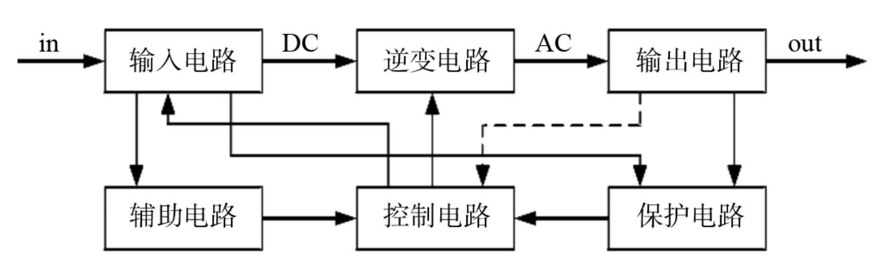
The structure of a sine wave voltage source solar photovoltaic inverter used in grid connected photovoltaic power generation systems is usually shown in Figure 1, mainly composed of a front-end DC/DC converter and a back-end DC/AC solar photovoltaic inverter. Its principle is to convert low-voltage direct current into high-voltage direct current based on boost technology, and then output 220V alternating current through the inverter circuit.
1. Inverter main circuit design
In photovoltaic power generation systems, as solar photovoltaic inverters require real-time control of DC bus voltage during normal operation under different lighting conditions, it is required that solar photovoltaic inverters have a wider DC input voltage range and ensure stable voltage output. Therefore, this design adopts IGBT switches with a wide input voltage range and high conversion efficiency at low loads, which generate on/off under corresponding pulse control, In order to obtain the required power frequency AC power at the load end, a single-phase bridge voltage source inverter main circuit using IGBT as a switching device is shown in Figure 2. In order to balance the instantaneous power difference between input and output, parallel electrolytic capacitors are usually needed in the system to solve the problem. Due to the short lifespan of electrolytic capacitors, the service life of solar photovoltaic inverters is severely limited. Therefore, Use long-lived thin film capacitors instead of electrolytic capacitors in the entire circuit design.
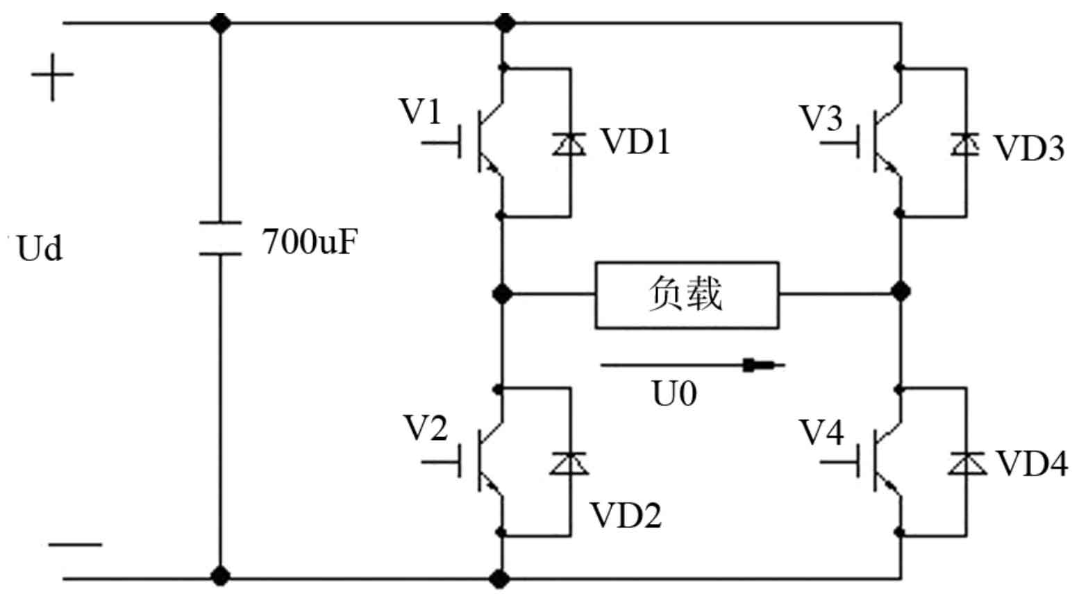
The load in Figure 2 is a resistive load. During operation, V1 and V2 are either on or off, and their working states complement each other. V3 and V4 work similarly to V1 and V2. The control process is as follows: in the positive half cycle of the output voltage U0, V1 is on, V2 is off, and V3 and V4 are alternately on and off. Due to the hysteresis of the current passing through the load compared to the output voltage, there is a certain interval in the positive half cycle of the voltage, The load current is positive. At this time, when V1 and V4 are conducting, U0 is equal to the voltage Ud; If V4 is turned off, U0=0. In another section, the load current is negative. When V1 and V4 are on, i0 is negative, so U0=Ud. If V3 is turned on and V4 is turned off, i0 passes through V3 and VD1, and U0 is still zero. Therefore, U0 can always obtain Ud and zero levels. Similarly, in the negative half cycle of U0, U0 obtains – Ud and zero.
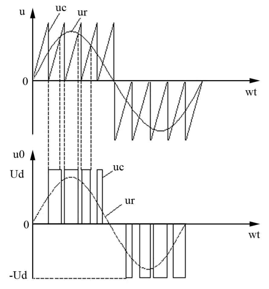
Figure 3 is a schematic diagram of controlling the on/off of V3 and V4. Ur is a sine wave modulated signal. In its positive and negative half cycle, the carrier Uc is a sawtooth wave with opposite polarity. The on/off of IGBT is controlled by the intersection of Ur and Uc. In the positive half cycle of Ur, V1 is on, V2 is off, and when Ur>Uc, V4 is on, V3 is off, and U0=Ud; Otherwise, V3 is turned on and V4 is turned off, at which point the U0 value is zero. Similarly, during the negative half cycle of Ur, V1 remains in the off state and V2 remains in the on state. When UrUc, make V3 turn off, V4 conduct, and U0=0, thus obtaining the PWM waveform U0.
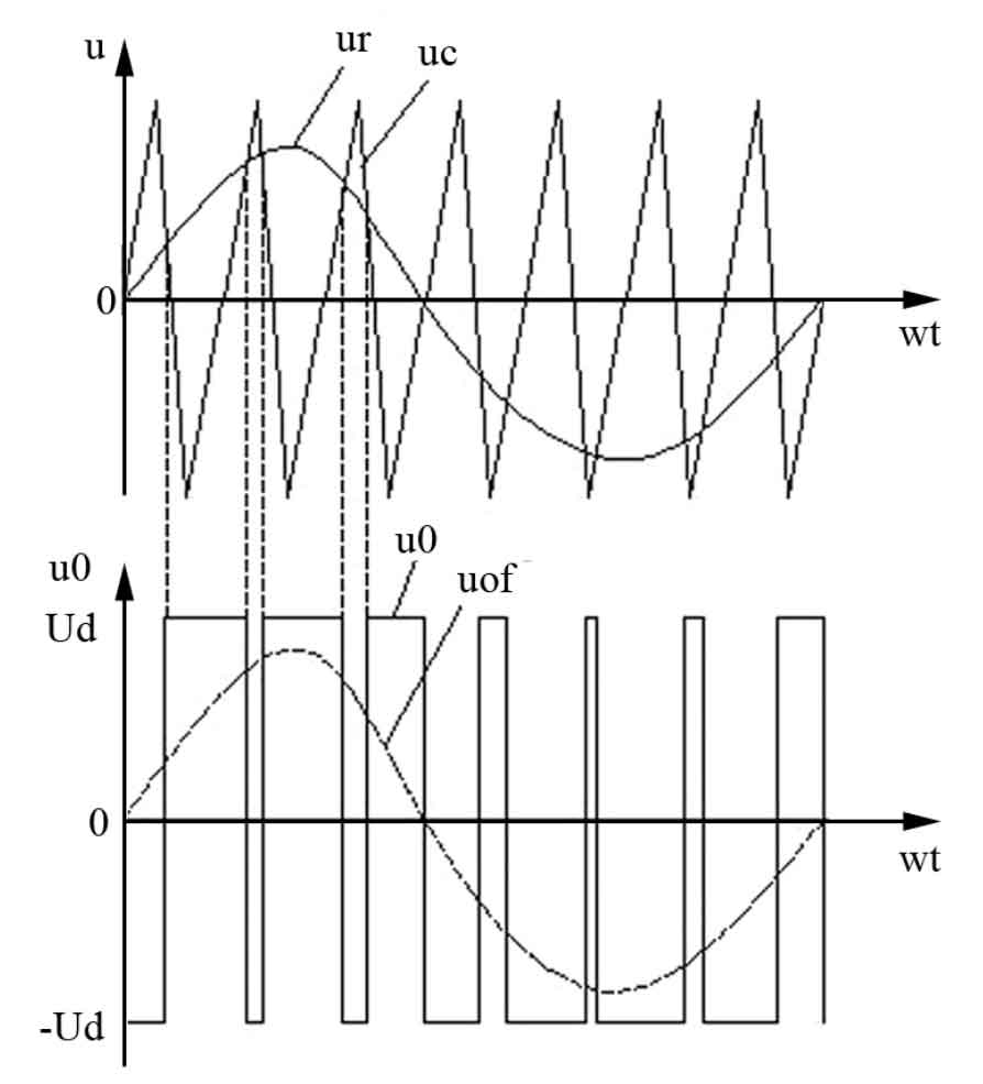
As shown in Figure 4, within one cycle of Ur, the output PWM wave only has two levels of ± Ud. In the positive and negative half cycles of Ur, the control law and unipolarity of each component are the same. That is, when Ur>Uc, V1 and V4 are given conduction signals, and V2 and V3 are given off signals. At this time, if i0>0, V1 and V4 are on, and if i0<0, VD1 and VD4 are on, Regardless of the situation, the output voltage U0=Ud. When Ur<Uc, provide a conduction signal for V2 and V3, and a shut-off signal for V1 and V4. At this time, if i0<0, then V2 and V3 are connected, and if i0<0, then VD2 and VD3 are connected. In either case, the output voltage U0=- Ud.
2. Design of DC/DC Control Circuit
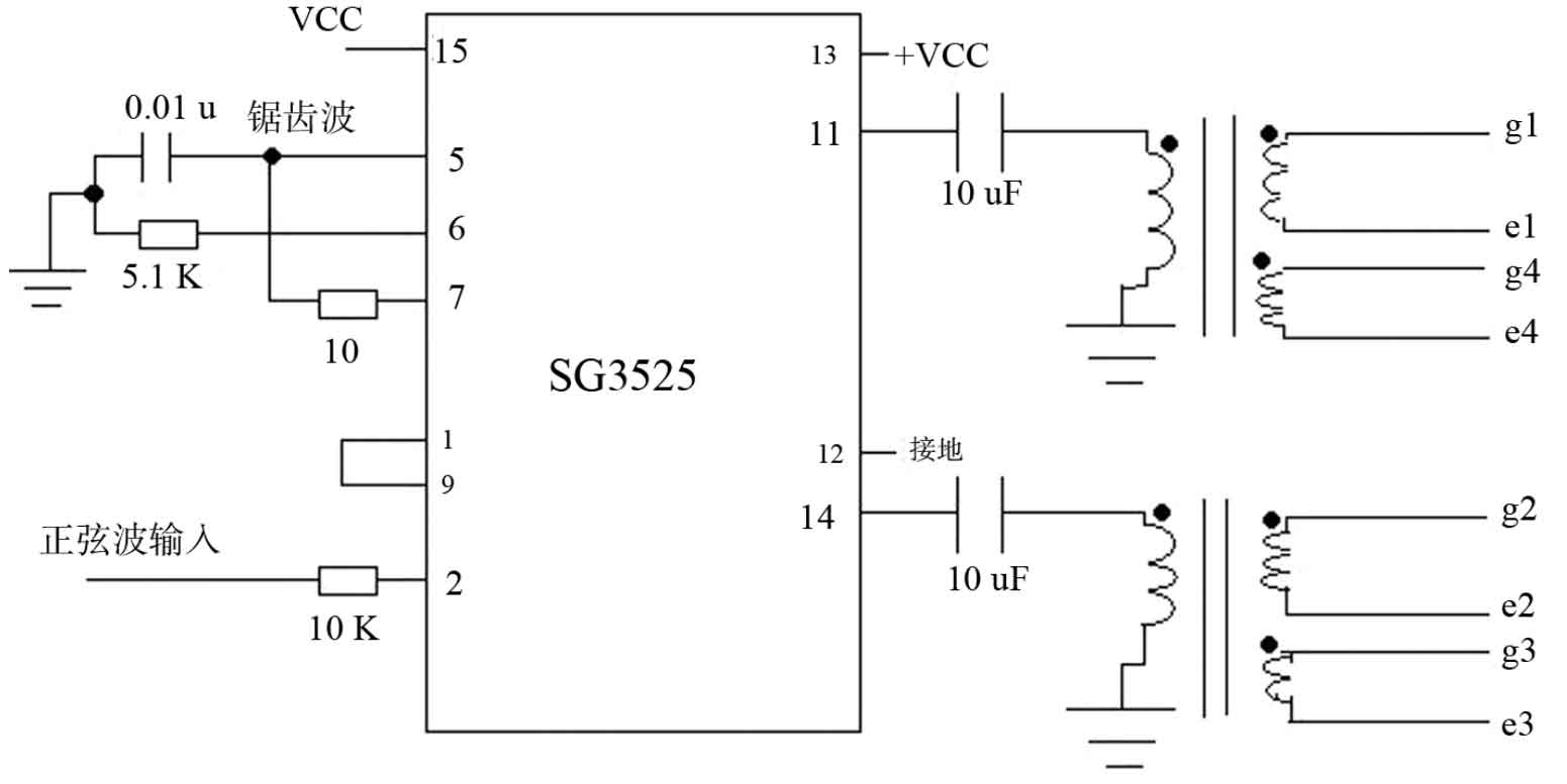
In this article, PWM adopts the control chip SG3525. The basic performance and working process of this chip refer to Xu Dongsheng’s article “Design of Solar Inverter Power Supply Based on SG3525A”. It contains an undervoltage locking circuit, a soft start control circuit, a PWM latch, and an overcurrent protection function, with adjustable frequency. The chip contains two pins, with a phase difference of 180 ° between pins 11 and 14, Connect a line to the transformer separately, and the capacitance between them blocks the direct current. It can generate four sets of control signals to control the on-off of switch tubes V1, V2, V3, and V4, respectively. This will obtain the required power frequency AC power at the load end. The source of the control signal is the sine wave generated by ICL8038 The sawtooth wave generated by SG3525 itself is generated together with the internal hardware circuit of SG3525. The hardware circuit of the control signal generated by SG3525 is shown in Figure 5.
3. Design of DC/AC control circuit
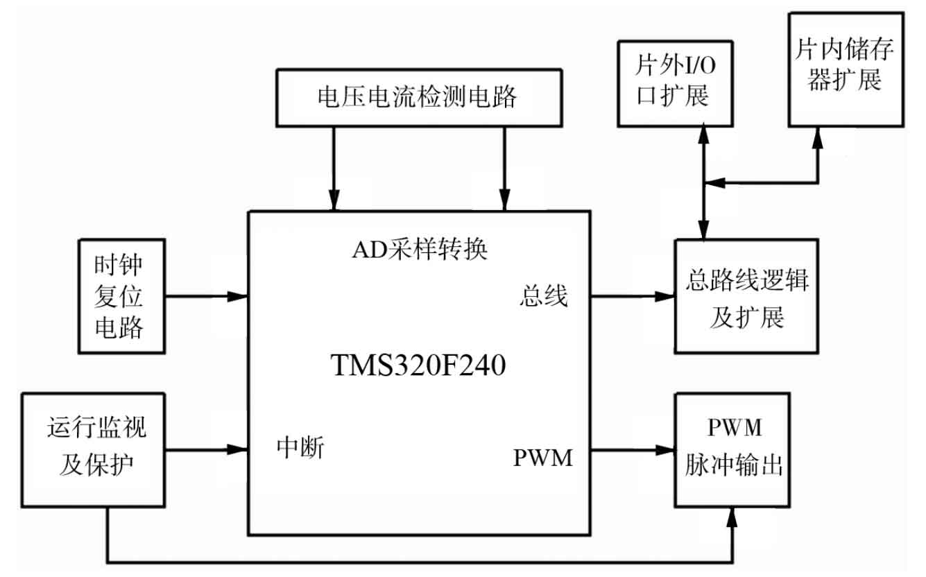
The structure of the DC/AC controller is shown in Figure 6. The core device is TMS320F240, which is mainly composed of voltage and current detection circuits. The voltage and current detection circuits mainly convert sine wave signals into TTL level signals that can be recognized by TMS320F240 through a comparator circuit, In order to achieve synchronization with the voltage signal of the power grid, the current measurement mainly uses the CSM300LT current sensor to measure the current under electrical isolation. The current signal is converted into a voltage signal, which is processed by the signal conditioning circuit and sent to the TMS320F240 chip.
4. Design of Sine Wave Generation Circuit
The generation of sine waves in this design is completed by the chip ICL8038, as shown in Figure 7.
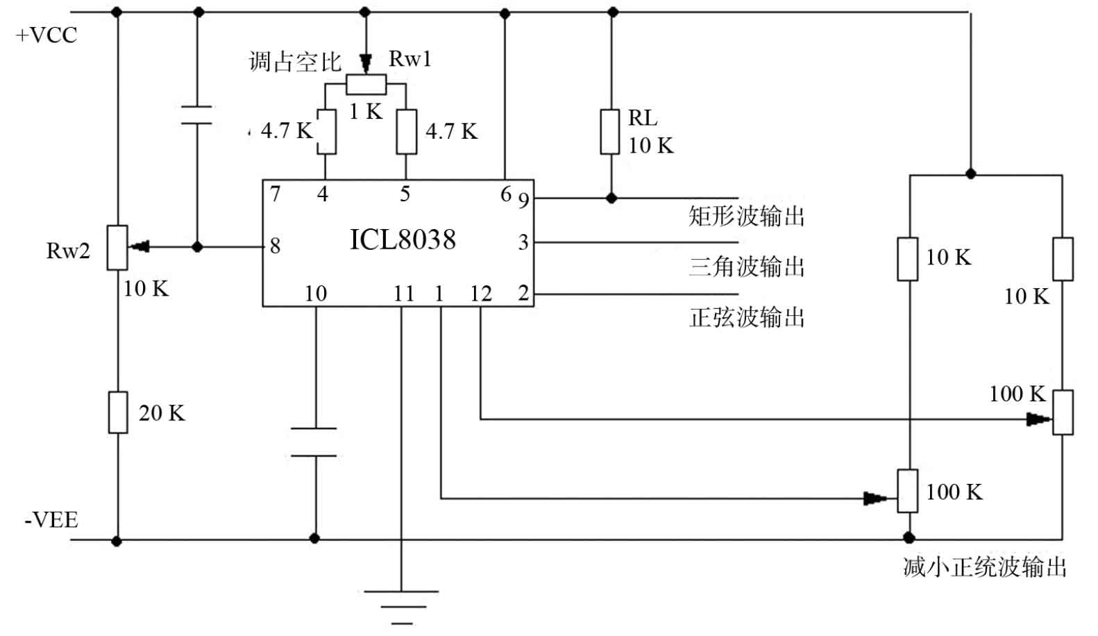
ICL8038 is an excellent integrated function generator that can be powered by a single power source, that is, pin 11 is grounded, pin 6 is connected to+VCC, and VCC is an external power source of 10V~30V; It can also be powered by dual power sources, with pin 11 connected to VEE and pin 6 connected to VCC, with a value range of ± 5V~± 15V. The adjustable frequency range is 0.01Hz~300kHz. To further reduce the distortion of the sine wave, this design combines two 100k Ω potentiometers and two 10k Ω resistors to form a circuit, By adjusting them, the distortion of the sine wave can be reduced to 0.5%, and by adjusting RW2, the ratio of the maximum to minimum oscillation frequency of the circuit can reach 100:1.
5. Parameter design of the main circuit switch tube
The switching frequency of the solar photovoltaic inverter is 30kHz, and the device operates in a hard switching state, which belongs to low voltage and high current situations. The switching speed and current tail phenomenon of the IGBT device make it unsuitable for this application. Therefore, the power field-effect transistor is selected as the main switch for the transformer in the solar photovoltaic inverter. The maximum voltage that the four tubes of the full bridge can withstand under normal working conditions is U1max, which is 50V, The current indicators are calculated as follows:
Current peak:
Average current value:
When analyzing the circuit loss, it was found that the conduction loss of the tube accounted for a large proportion, so the tube with low conduction resistance and high rated current was selected. In the end, the FSAM20SL60IGBT tube from American Express Company was selected for this circuit, with a rated current of 20A and a withstand voltage of 60V, which reduced the cost by 40% compared to similar devices and reduced the overall size by nearly 30%
6. Experimental Results and Conclusion
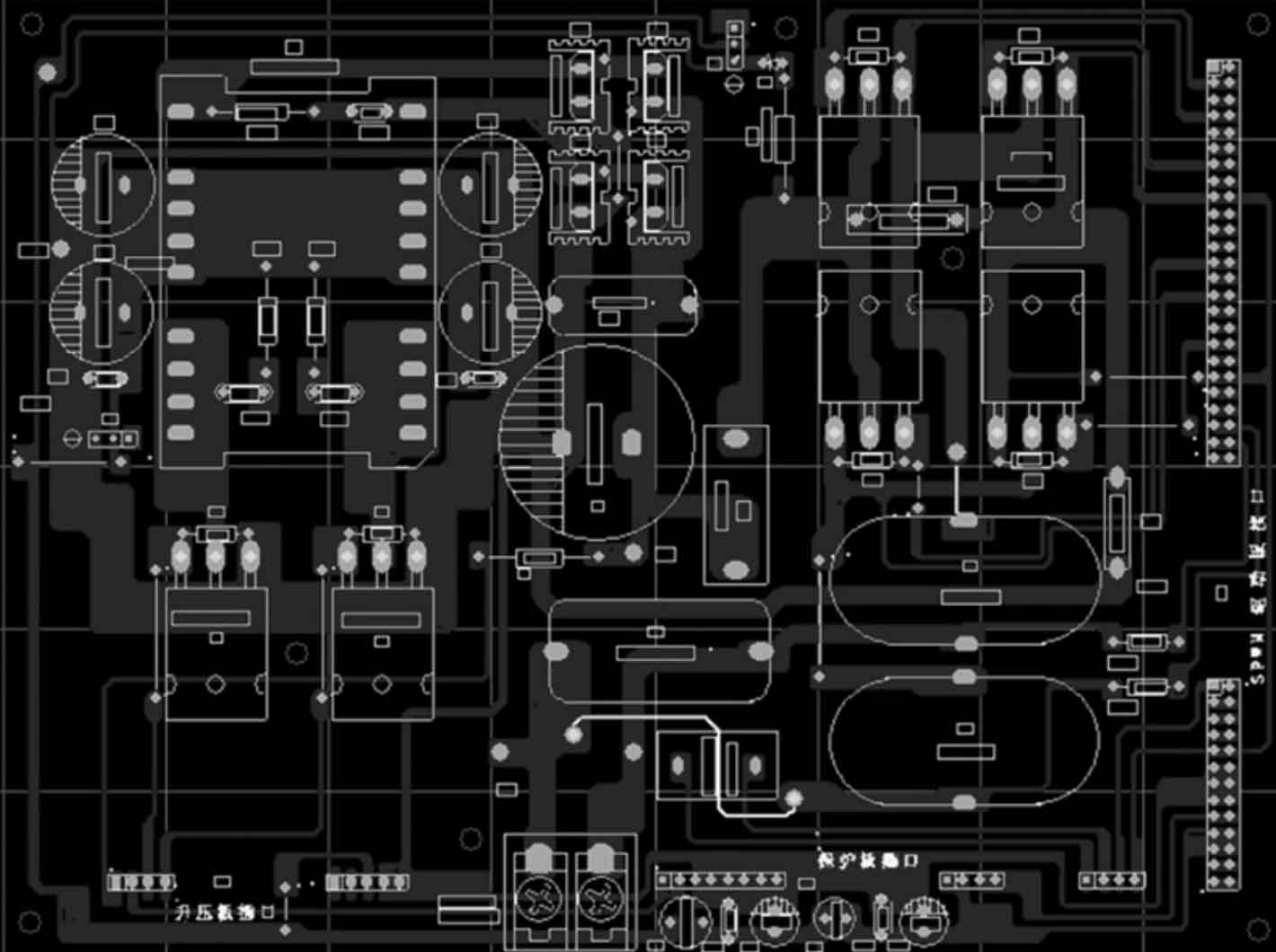
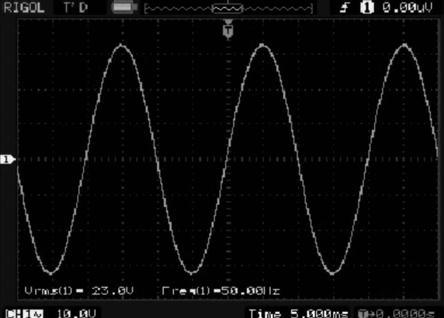
In order to verify the correctness of the above solar photovoltaic inverter design, a solar photovoltaic inverter circuit board was made, as shown in Figure 8. The output voltage waveform with resistive load is shown in Figure 9. It can be seen that the output voltage is about 230V, the harmonic content is less than 3%, the frequency is 50Hz, the waveform is smooth, and there are no burrs, It can be used as AC power for supply equipment. The measured conversion efficiency reaches 95.6% when the output power is 100W, which is fully suitable for civilian use and has good promotion prospects.
Based on the characteristics of solar photovoltaic inverters, this article uses key components TMS320F240, SG3525, and ICL8038 to research and design solar photovoltaic inverters. The basic functions of the system are relatively complete, the cost is low, the development cycle is short, and it is suitable for market promotion.