In the previous chapters, we introduced the mathematical model, circuit topology, control algorithm, and other contents of the inverter. We will analyze the hardware and software control parts of the three-phase photovoltaic inverter prototype, including component parameter design, introduction of the main control chip, and important circuit design, etc.
1. Hardware structure of three-phase photovoltaic grid connected inverter
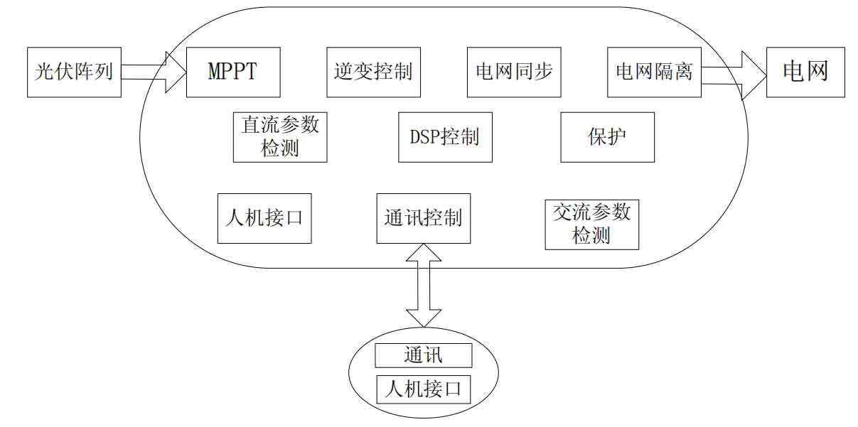
The functional modules of the three-phase photovoltaic grid connected inverter system are shown in Figure 1. The output of the solar panel meets the inverter requirements after passing through a boost circuit. The MPPT module can utilize the inverter with the maximum photovoltaic DC, and generate three-phase grid connected current with the same frequency, phase, and amplitude as the grid voltage through the inverter and synchronization module. During operation, the protection module is used to prevent damage to components and ensure stable and safe operation of the system.
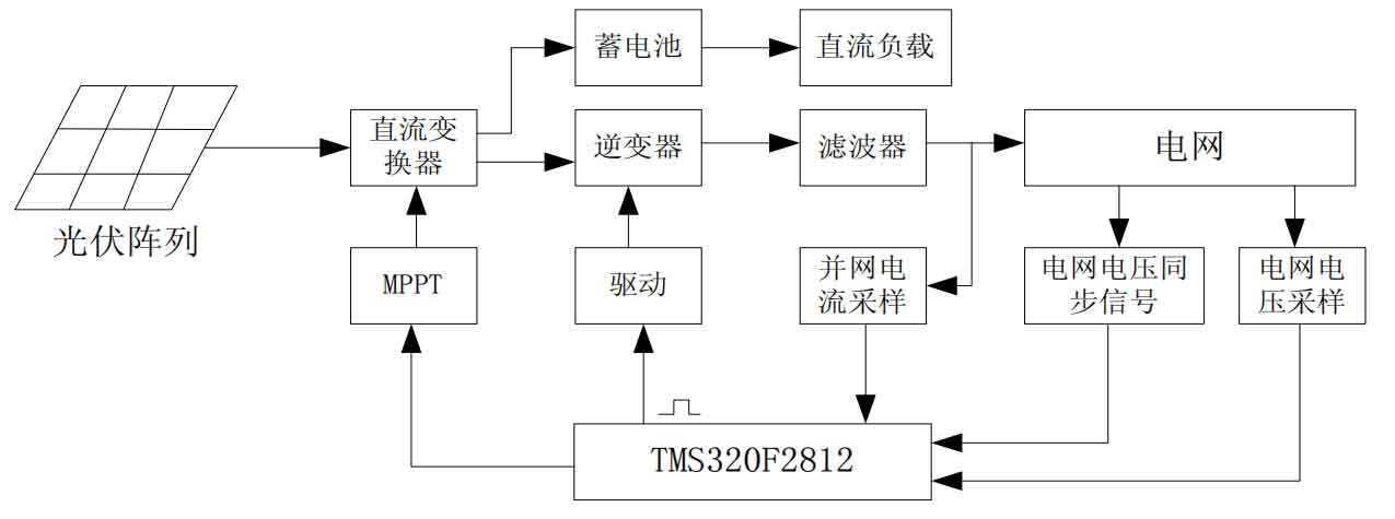
The hardware structure of the three-phase photovoltaic grid connected inverter is shown in Figure 2. TMS320F2812 serves as the main control chip, controlling the inverter bridge arm to synchronize the output current with the grid voltage. The filter processes the output current to eliminate harmonic effects. By collecting grid connected current and grid voltage, it is sent to the A/D interface of the DSP. After SVPWM control, a PWM drive waveform is generated, and the power switch is controlled to turn on and off through an isolation circuit.
2. Design of main circuit components
2.1 Selection of Power Device IGBT
For power inverter circuits, common power switches include MOSFET, IGBT, and IPM modules. IGBT not only has the advantages of fast on/off speed and low driving power of MOSFETs, but also has the advantages of high blocking voltage and large capacity of bipolar power transistors. Therefore, IGBT has become the preferred power device for inverter circuits, and its application fields are also very wide. This design selected Xiantong’s SGH20N120RUFD model IGBT, which comes with a reverse diode.
2.2 Selection of DC side capacitors
In order to buffer the energy exchange between the DC side and the grid side, the current at the moment of switch switching, and suppress the influence of harmonic voltage on the DC side, the larger the design, the better. However, if the design is too large, it will affect the tracking speed. So the DC side capacitance is calculated and selected based on the fluctuation of the DC bus voltage, and the calculation formula is:

Where IN is the rated phase current, Δ T is the switching cycle, Δ Udc is allowed to fluctuate, so we set it to 15%.
The rated phase current is:

Frequency fc=20 KHz, Δ T=5X10 ^ -5s, Udc=700 V, calculated by substituting into the formula, C1=40.9 uF can be obtained. In practice, a certain margin should be left, so a capacitor larger than the calculated value should be selected.
2.3 Selection of AC side LC filter
(1) Selection of filtering inductance
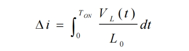
The design of the inductor will affect the size of the output ripple, so we first consider the ripple coefficient. According to the volt ampere relationship V=Ldi/dt, it can be concluded that:
When V0 (T)=Vgmax, the ripple reaches its maximum, then:
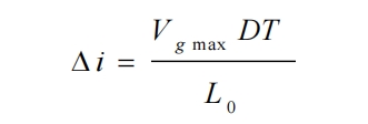
Where T is the switching cycle and D is the duty cycle.
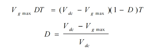
According to the principle of volt second:
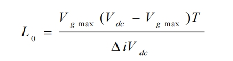
By combining the above equation, it can be concluded that:
In order to meet the requirement that the actual ripple is less than the limit value, the inductance value should generally be greater than the calculated value. At the same time, considering the cost and volume of the inductance, we ultimately chose the inductance value of 2.8mH.
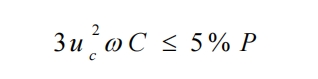
(2) Filter capacitor selection
The magnitude of the reactive power output by the system is determined by the filtering capacitor. Generally, the reactive power does not exceed 5% of the rated power
In general, we believe that uc is approximately equal to ug, so C ≤ 5% x pn/(3x 2 π fug ^ 2)=30 uF. In practice, we choose the capacitance value as C=10 uF.
3. Hardware circuit design of three-phase photovoltaic grid connected inverter system
3.1 Selection of Control Chips
The most important thing in the entire photovoltaic grid connection control process is to control the inverter to synchronize its output with the grid voltage, which requires high accuracy and speed of the system. The control chip TMS320F2812 produced by TI company has the advantages of fast speed and high accuracy, and is applied in various neighborhoods. In this design, DSP will also be used as the control chip to improve the efficiency and accuracy of photovoltaic grid connection. The main advantages of TMS320F2812 are as follows:
(1) The CPU has a main frequency of up to 150MHz and a time cycle of 6.67ns.
(2) Equipped with SRAM and Flash, it reduces complexity.
(3) A high-performance 32-bit central processing unit.
(4) It has multiple external devices, such as CAN, EV, ADC, etc.
(5) Externally expandable 1M x 16 bit storage space.
(6) There are two event managers, each EV has three comparison units, which can generate 6 independent PWM waveforms, and the pulse width can be changed through programming.
3.2 Design of Drive Isolation Circuit
Due to the modulation waveform output by DSP having a maximum voltage of 3.3V, which does not meet the voltage required for normal power transistor switching, IGBT switching generally requires a voltage of around 10-20V. So, in order to ensure the normal operation of the power transistor, we must use a driving circuit to achieve the normal operation of the power transistor.
We will use the commonly used motor driver chip IR2235 to drive power switches with a voltage below 1200V. Its internal structure is shown in Figure 3: it contains three sets of high voltage and low voltage drive circuits, and the input signal is well compatible with TTL and CMOS. At the same time, it has strong protection functions, can close six channels and output fault information.
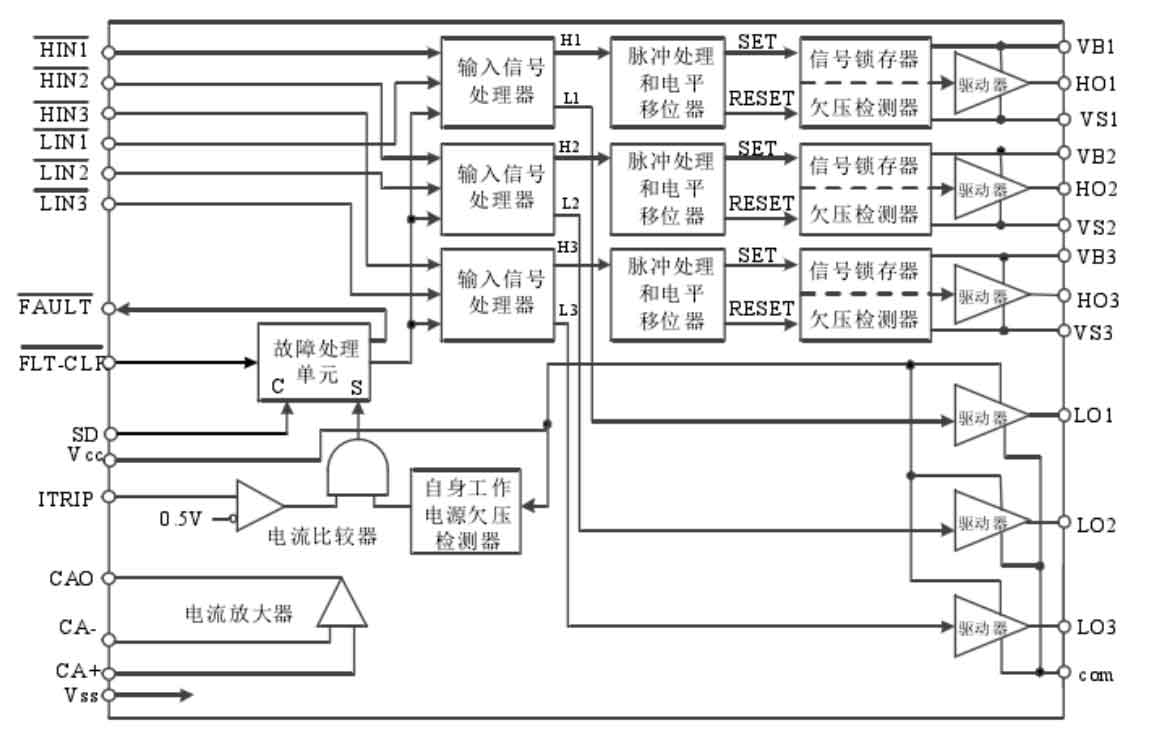
Under normal working conditions, 6 PWM waves are converted and processed into 6 pulse signals through 3 input signals. The 3 low-voltage signals are amplified by power and sent to the switching transistor. The signals on the high-voltage side are processed into 3 driving pulses through 3 pulse processing and level shifting, and finally added to the gate source of the switching transistor after being locked and amplified by power. If a fault is detected, the comparator will flip, causing the faulty logic unit to output a low level, thereby turning off the pulse output and causing the gate source pole to reverse bias and cut off, in order to protect the power transistor and avoid damage.
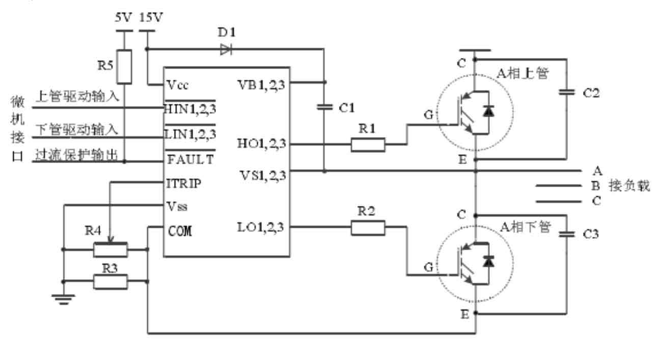
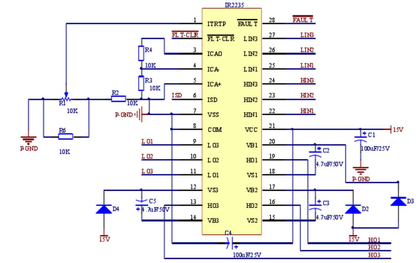
The common application circuit of IR2235 is shown in Figure 4, where R3 is overcurrent sampling and C1 is bootstrap capacitor. In the experiment, we took 4.7 μ F. The driving circuit we designed is shown in Figure 5. By changing R1 to set the overcurrent value, R 6 is for overcurrent detection, and D 1 is the fast recovery diode FR 107, which has a withstand voltage of 1000V.
During the operation of the inverter bridge, if the switch tube is damaged, the direct current of the bus will pass through IR2235, causing damage. Therefore, isolation treatment must be carried out between DSP and IR2235 to ensure that the driving chip is not burned.
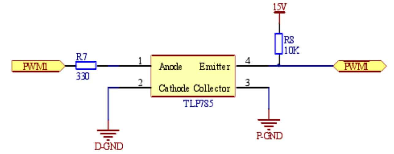
In practical control, to prevent the main circuit from affecting the control circuit and the analog circuit from affecting the digital circuit, the analog circuit will be isolated from the control circuit, usually using optocoupler isolation. Due to the high frequency pulse signal generated in the design, we used Toshiba TLP 785 to isolate the PWM signal and control signal. Optocoupler isolation is a single channel isolation, so we need six optocouplers. The design of optocoupler isolation is shown in Figure 6.
3.3 Design of Sampling Circuit
For voltage sampling, we need to sample the grid voltage and inverter output voltage separately, so we can use the same voltage acquisition circuit to collect the two voltages. The only difference is that the grid voltage is determined by the grid, and the output voltage is determined by the inverter output after passing through a filter. The sampling circuit is shown in Figure 7.
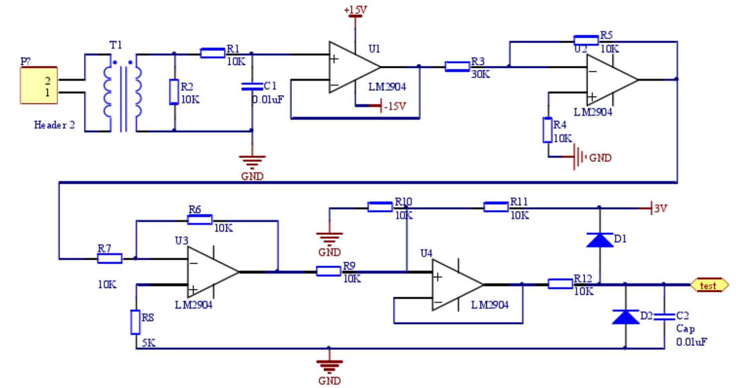
Firstly, we need to obtain the required voltage after passing through a step-down transformer, and the voltage obtained after passing through a filter, emitter follower, and proportional amplification circuit should be within ± 1.33V. Due to the fact that negative voltage DSP cannot recognize it, we need to convert the negative voltage through an addition circuit into a recognizable positive voltage. Finally, after passing through an emitter follower and a voltage regulator protection tube, the voltage is sent to the DSP’s A/D interface for processing.
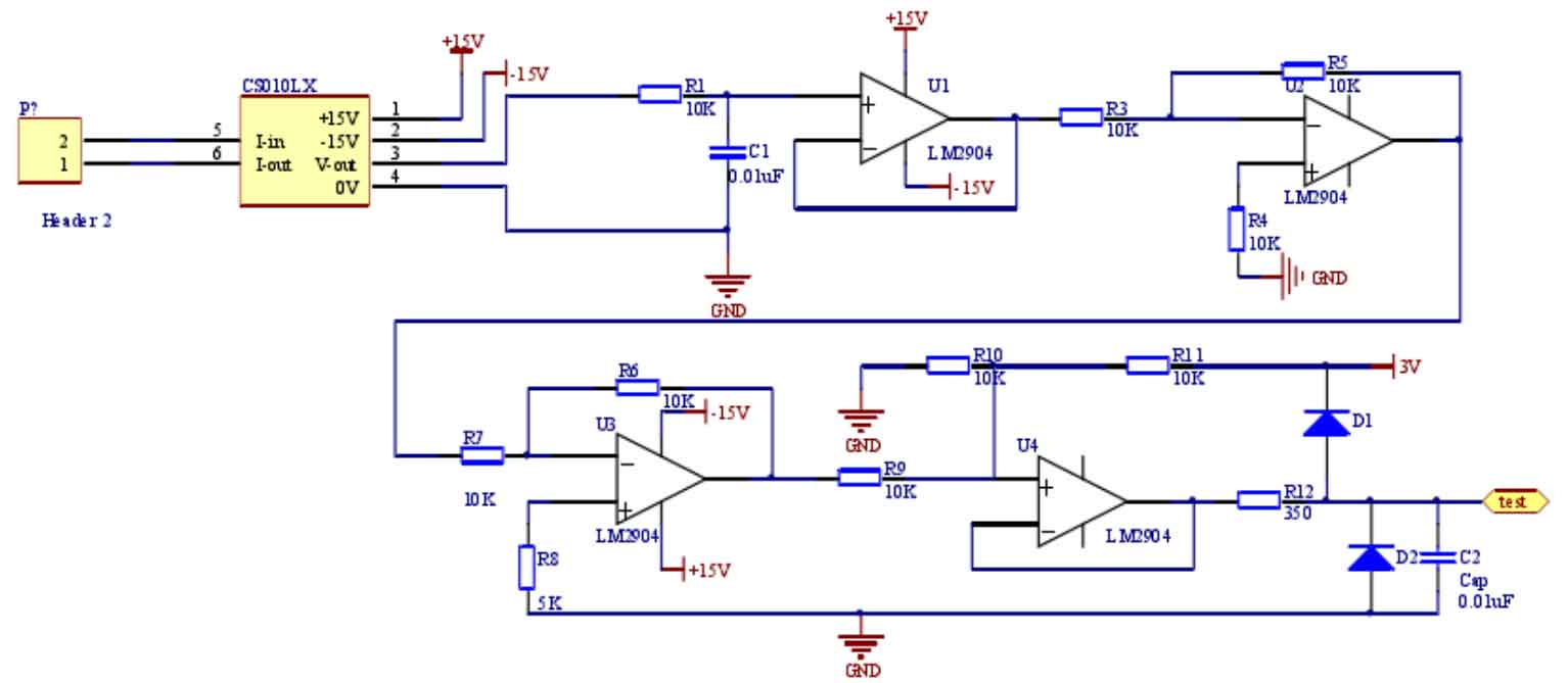
For current collection, we will use a Hall current sensor CS010LX in series in the circuit to convert the current signal from the original side to the amplitude side voltage signal. After the voltage collection circuit we designed above, the analog signal will be converted into a digital signal through DSP. The CS010LX type sensor has strong interference, low power temperature drift, wide frequency band and small volume. The primary current is 5A, and it can detect up to 10A. The amplitude voltage is 4 ± 1% V, and the DC power supply voltage is ± 12~± 15V. The current sampling circuit is shown in Figure 8.
3.4 Grid voltage zero crossing detection circuit
In a grid connected system, the existence of a phase-locked loop can ensure that the output grid connected current and the phase and frequency of the grid voltage are the same, which is also a basic requirement for grid connection. In this design, we will use hardware detection and phase-locked software together to obtain a synchronization signal with the grid voltage through a zero crossing detection circuit, and then send this synchronization signal to the CAP interface of 2812. Set a certain timer as the time reference to capture the rising edge. Record the customized timer value every time it is captured, and set an interrupt. The difference between two adjacent timers is the frequency value of the grid voltage. Finally, take the calculated period value as the period value of the sine voltage, so that the frequency of the grid connected current and the grid voltage can be the same. Each interruption during recording corresponds to a zero crossing point of the voltage. We can adjust the sine to point towards the phase of 0 ^ 0, thus achieving the same phase.
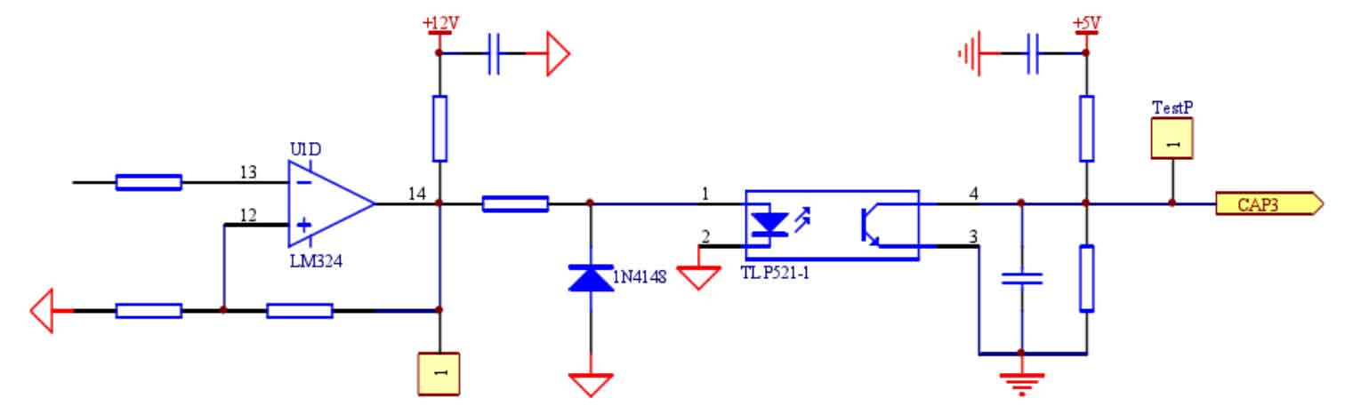
On the hardware of three-phase photovoltaic grid connected inverters, we first convert the grid voltage into a low-voltage signal of ± 1.5V through Hall sensors. After passing through a voltage follower and a zero crossing hysteresis comparator, the obtained signal is isolated and filtered by optocouplers and sent to the DSP. We add a voltage regulator before the optocoupler to prevent damage to the optocoupler due to excessive amplitude. The zero crossing detection circuit of the power grid voltage is shown in Figure 9.
3.5 Protection circuit design
In the hardware design of three-phase photovoltaic grid connected inverters, we usually design some protection circuits to ensure the normal operation of the system, while also avoiding damage to components. The protection circuits generally have overvoltage and overcurrent protection.
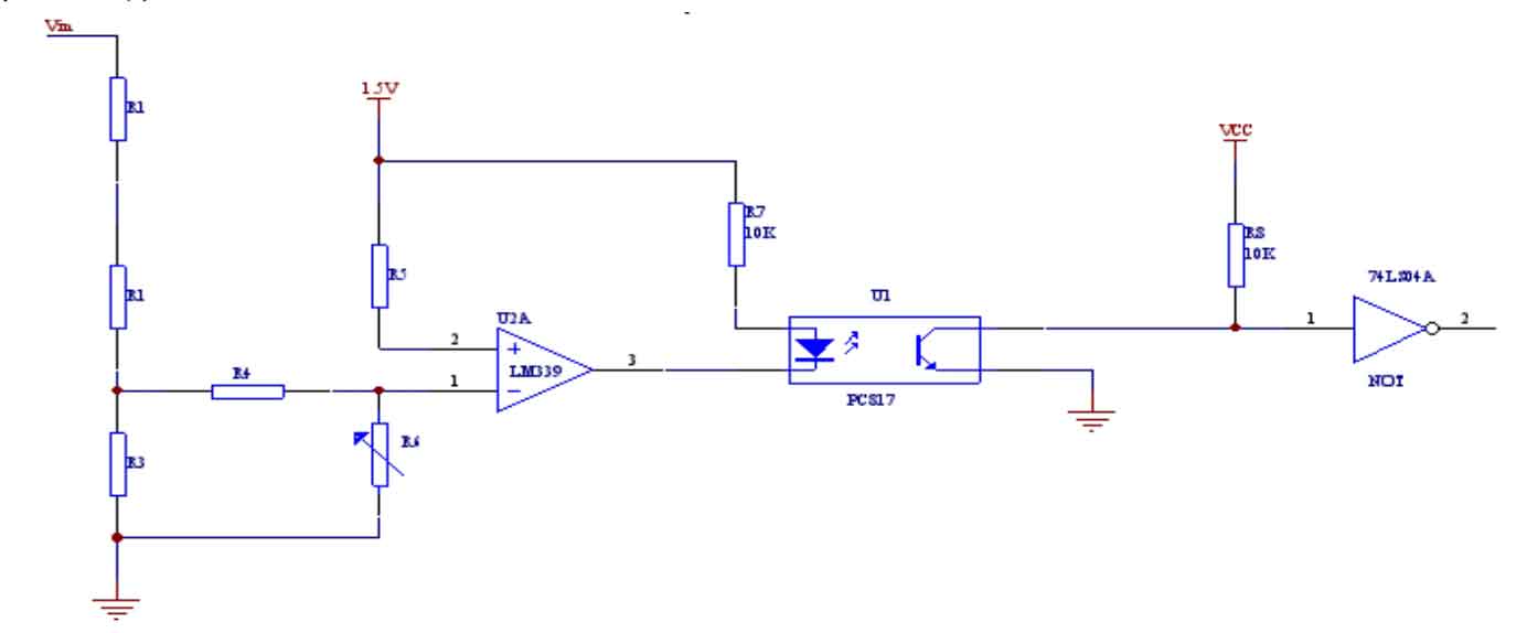
Overvoltage protection is when the voltage is unstable and exceeds the maximum voltage required for normal circuit operation, the protection circuit will send a signal to the DSP to stop working. The overvoltage protection circuit is shown in Figure 10. The voltage signal obtained by dividing the voltage through three resistors is compared with the reference voltage. If it is higher than the reference voltage, a warning signal will be output, causing the DSP to stop working.
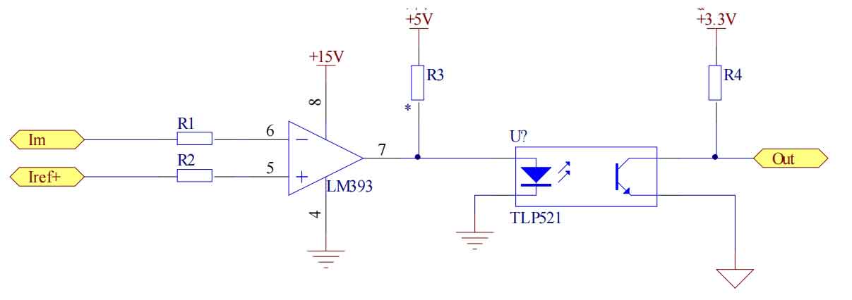
The overcurrent protection circuit is similar to the overvoltage protection circuit, which compares the input current signal with the reference current signal. If it is higher than the reference value, it will also output a warning signal, causing the DSP to stop working. The overcurrent protection circuit is shown in Figure 11.
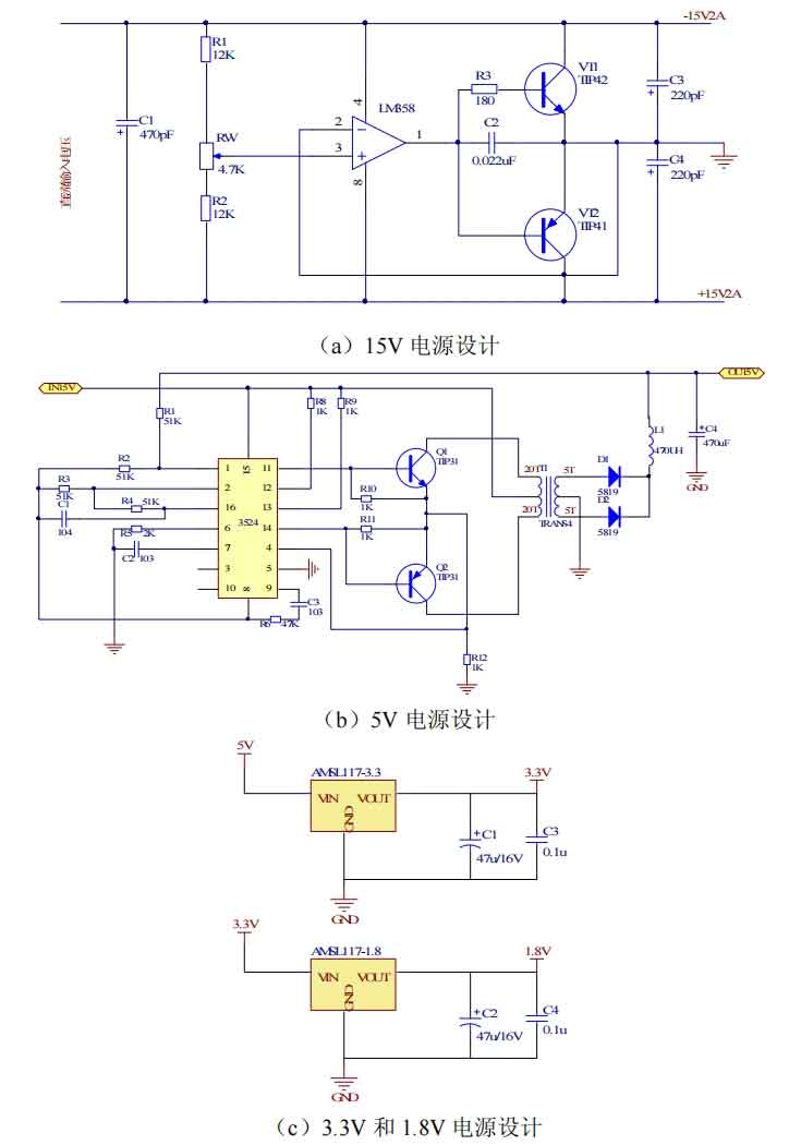
3.6 Power circuit design
In order to ensure the normal operation of each circuit and chip, it is necessary to design different voltage circuits to increase different voltages. For example, the normal working voltage of the chip is+5V, the working voltage of the driver circuit is+15V, the working voltage of the DSP core is 1.8V, and the working voltage of the interface is 3.3V. Therefore, we have designed relevant voltage circuits, including 5V, 15V, 1.8V, and 3.3V voltages. The DC input terminal is directly supplied with voltage by the battery. The 5V power supply design has a 15V power supply as the input voltage. The design of the power circuit is shown in Figure 12.