
In the context of renewable energy applications and modern power system development, parallel operation systems for single phase inverters have become increasingly prevalent. These systems involve multiple single phase inverters connected in parallel to supply power to a common load, enabling high-capacity output, redundancy, and enhanced flexibility and reliability. This design focuses on a photovoltaic power generation background, utilizing STM32 microcontrollers as the main control chips and single-polarity SPWM modulation to develop a dual-inverter grid-connected power supply system centered on single-phase full-bridge inverter circuits. The system comprises STM32 control circuits, AD7606 sampling circuits, single-phase inverter drive circuits, filtering circuits, and buffer circuits. Compared to other control methods, this design offers superior redundancy, simplicity, cost-effectiveness, and improved reliability. Testing confirms that the system can output currents ranging from 1 A to 3 A with a frequency of 50 ± 0.2 Hz, a total harmonic distortion (THD) rate below 2%, and the ability to distribute current in varying proportions.
The core of this work is the implementation of a parallel system for single phase inverters, which addresses challenges in power quality and load sharing. I have designed the system to ensure stable operation under varying load conditions, with a focus on minimizing harmonic distortion and optimizing efficiency. The use of STM32 microcontrollers allows for efficient signal processing and flexible control, while the single-polarity SPWM method ensures precise modulation. This approach is particularly suitable for single phase inverter applications in distributed energy systems, where reliability and performance are critical.
In the following sections, I will detail the system design, including comparisons of control strategies, theoretical analyses, circuit implementations, and test results. Key aspects such as the selection of components for the single phase inverter, control algorithms, and parallel operation techniques will be explored. Tables and formulas will be used extensively to summarize design parameters and performance metrics, providing a comprehensive overview of the single phase inverter parallel system.
Scheme Comparison and Selection
When designing a parallel system for single phase inverters, the choice of control units and strategies is crucial. I evaluated various options to achieve optimal performance, reliability, and cost-efficiency for the single phase inverter setup.
Main Control Unit Selection
For the main control unit, I compared Digital Signal Processors (DSPs) and STM32 microcontrollers. DSPs are known for their computational power and flexibility in handling complex algorithms, but their sequential execution model can limit processing speed in inverter control applications. In contrast, the STM32 microcontroller, based on the ARM architecture, offers high performance, low cost, and efficient signal processing. It features low power consumption, high clock frequencies, ease of operation, and stability. Specifically, the STM32 provides six PWM output channels and three duty cycle generators, which help maintain low THD in the single phase inverter output. Additionally, its threshold interval control function prevents simultaneous conduction of upper and lower bridges, reducing the risk of short circuits and enhancing system safety. Therefore, I selected the STM32 microcontroller as the main control unit for this single phase inverter design.
Single Inverter Control Strategy Selection
To ensure good dynamic and steady-state output characteristics for the single phase inverter, I considered control strategies such as one-cycle control, deadbeat control, intelligent control, and voltage-current double-loop PI control. Intelligent control techniques offer robustness and adaptability without requiring precise mathematical models, but their accuracy can be affected by human factors. On the other hand, the voltage-current double-loop PI control strategy uses an inner current loop and an outer voltage loop. The current loop widens the system bandwidth, accelerates dynamic response, and reduces harmonic content, while the voltage loop stabilizes the output voltage by minimizing the error between the load voltage and the reference voltage. This method provides high control precision, making it suitable for the single phase inverter in this design.
Dual Inverter Parallel Control Strategy Selection
For parallel operation of single phase inverters, I evaluated centralized, decentralized, and master-slave control methods. Master-slave control requires communication between inverters, which can lead to issues like communication failures affecting system monitoring and control. Centralized control relies heavily on a single module, resulting in poor redundancy. In contrast, decentralized control using the droop method utilizes local information from each power source without additional interconnecting signal lines. By collecting output parameters and applying a predefined control strategy, multiple single phase inverters can operate collaboratively. This approach offers excellent redundancy, simplicity, cost savings, and increased reliability, making it the preferred choice for this single phase inverter parallel system.
Overall System Description
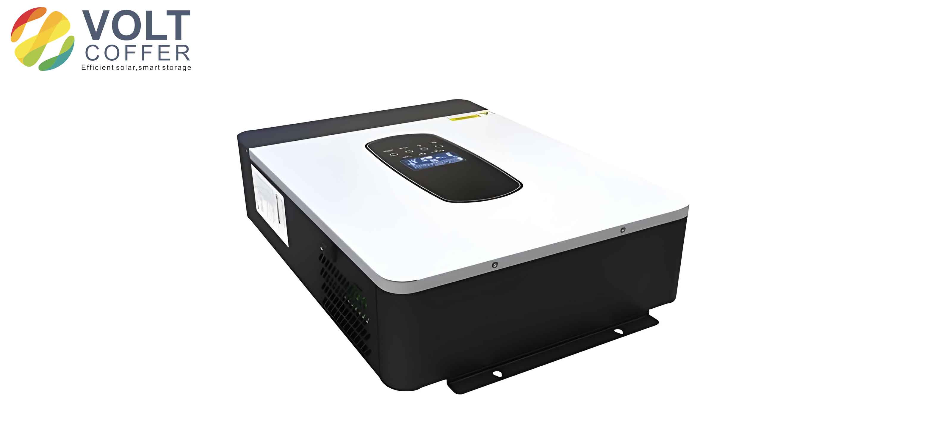
The grid-connected power supply system includes STM32 microcontroller modules, single-phase full-bridge inverter circuits, synchronous phase modules, IR2110S drive modules, and AD7606 sampling modules. With an input DC voltage of 30 V, two DC/AC single-phase full-bridge inverter circuits are connected in parallel to produce an output voltage RMS of 24 V and a maximum output current RMS of 3 A. The STM32 generates single-polarity SPWM waves to control the MOSFETs in the single phase inverter, while the synchronous phase-locking module ensures phase synchronization between the master and slave units. The AD7606 sampling module provides feedback signals, and the microcontroller employs voltage-current double-loop PI control to adjust the SPWM waves, regulating the output current and voltage. The master unit controls the output voltage, and the slave unit controls the output current, implementing a double-loop control that enhances system stability. Testing shows that the system achieves a load line current of 1–3 A, a frequency of 50 ± 0.2 Hz, a THD below 2%, and proportional current distribution. The load and voltage regulation rates are low, with an average overall efficiency of 91% and up to 94% for a single single phase inverter.
| Control Aspect | Option 1 | Option 2 | Selected Scheme |
|---|---|---|---|
| Main Control Unit | DSP | STM32 | STM32 |
| Single Inverter Control | Intelligent Control | Voltage-Current PI | Voltage-Current PI |
| Parallel Control | Centralized | Decentralized Droop | Decentralized Droop |
Theoretical Analysis and Calculation
The theoretical foundation for the single phase inverter system involves control strategy design and parameter calculations to ensure optimal performance. I have derived formulas for key components such as capacitors, inductors, and control loops.
Single Inverter Control Strategy Design
For a single phase inverter operating independently, I implemented a voltage-current double PI control strategy targeting the output voltage \( U_o \) and inductor current. The control block diagram includes feedback for load current to account for load adjustments. The transfer functions and PI controller parameters are designed to minimize error and enhance stability. The output voltage and current relationships can be expressed using Laplace transforms, with the PI controllers compensating for deviations.
The voltage loop controller aims to regulate the output voltage, while the current loop improves dynamic response. The control law for the single phase inverter can be summarized as:
$$ G_c(s) = K_p + \frac{K_i}{s} $$
where \( K_p \) and \( K_i \) are the proportional and integral gains, respectively. For the single phase inverter, the closed-loop transfer function is derived to ensure stability and fast response. The output voltage \( U_o(s) \) in terms of the reference voltage \( U_{o,ref}(s) \) and load current \( i_o(s) \) is given by:
$$ U_o(s) = \frac{G_c(s) G_v(s)}{1 + G_c(s) G_v(s)} U_{o,ref}(s) – \frac{Z_o(s)}{1 + G_c(s) G_v(s)} i_o(s) $$
where \( G_v(s) \) is the plant transfer function and \( Z_o(s) \) is the output impedance. For the single phase inverter with an LC filter, \( G_v(s) = \frac{1}{LCs^2 + RC s + 1} \), where \( L \) and \( C \) are the filter components, and \( R \) represents losses.
Dual Inverter Parallel and Grid-Connected Control Strategy Design
In the parallel operation of two single phase inverters, the control strategy integrates phase-locked loops (PLL), second-order generalized integrators (SOGI), SPWM, and PI controllers to form a precise closed-loop system. This ensures high-quality AC voltage output from DC input and accurate control of voltage and current. The use of IPD082N10N3G MOSFETs, with a maximum current rating of 80 A, supports reliable operation under various load conditions for the single phase inverter system.
The droop control method for parallel single phase inverters adjusts the output power based on local measurements without communication. The active power \( P \) and reactive power \( Q \) are used to control frequency and voltage amplitude, respectively. The droop equations for the single phase inverter are:
$$ f = f_0 – k_p (P – P_0) $$
$$ V = V_0 – k_q (Q – Q_0) $$
where \( f_0 \) and \( V_0 \) are the nominal frequency and voltage, \( k_p \) and \( k_q \) are droop coefficients, and \( P_0 \) and \( Q_0 \) are reference power values. For the single phase inverter system, this ensures proportional power sharing and stability.
The overall control框图 for the dual single phase inverter parallel system involves coordinate transformations, PI regulation, and modulation. The output voltage and current are transformed to dq coordinates for decoupled control, and inverse transformations generate the SPWM signals. This approach enhances the performance and stability of the parallel single phase inverter operation.
| Parameter | Symbol | Value |
|---|---|---|
| Nominal Frequency | \( f_0 \) | 50 Hz |
| Nominal Voltage | \( V_0 \) | 24 V |
| Droop Coefficient (Active) | \( k_p \) | 0.1 Hz/W |
| Droop Coefficient (Reactive) | \( k_q \) | 0.01 V/VAr |
Circuit and Program Design
The hardware design for the single phase inverter system includes the main circuit, component selection, drive circuits, sampling circuits, auxiliary power supplies, and software programming. I have carefully chosen components to meet the requirements for efficiency, reliability, and cost.
Main Circuit and Component Selection
The main circuit of the single phase inverter consists of a full-bridge topology with MOSFETs, LC filters, and DC-link capacitors. The design focuses on minimizing losses and harmonic distortion for the single phase inverter.
Input Filter Capacitor Design
To suppress AC harmonics on the DC side, the DC-link capacitor value is determined by:
$$ C_{dc} > (6 \sim 8) \frac{T}{2 R_{dc}} $$
where \( T \) is the output voltage period of the single phase inverter, and \( R_{dc} \) is the equivalent resistance on the DC side at rated power. Ignoring transmission losses, \( R_{dc} \) is derived from the relationship between transmission power and DC voltage:
$$ R_{dc} = \frac{U_{dc}^2}{P} $$
For a DC voltage \( U_{dc} = 50 \, \text{V} \) and power \( P = 100 \, \text{W} \), \( R_{dc} = \frac{50^2}{100} = 25 \, \Omega \). With \( T = 0.02 \, \text{s} \) for 50 Hz, the capacitor range is:
$$ C_{dc} > (6 \sim 8) \frac{0.02}{2 \times 25} = (6 \sim 8) \times 0.0004 = 2400 \, \mu\text{F} \sim 3000 \, \mu\text{F} $$
I selected \( C_{dc} = 3000 \, \mu\text{F} \) using three 1000 μF electrolytic capacitors in parallel, each rated for 100 V.
Filter Design
For the single phase inverter output, I used an LC filter to attenuate switching harmonics. The inductor value is determined by the current ripple, which is typically 15% of the rated current. For a rated power of 100 W, output voltage 24 V, and efficiency η = 0.9, the rated current is:
$$ I_{\text{rated}} = \frac{P}{U \cdot \eta} = \frac{100}{24 \times 0.9} \approx 4.63 \, \text{A} $$
The current ripple ΔI is:
$$ \Delta I = 0.15 \times I_{\text{rated}} = 0.15 \times 4.63 \approx 0.69 \, \text{A} $$
The inductor \( L_o \) must satisfy:
$$ L_o > \frac{U_{dc}}{4 \Delta I \cdot F} $$
where \( U_{dc} = 50 \, \text{V} \) and switching frequency \( F = 15 \, \text{kHz} \). Thus,
$$ L_o > \frac{50}{4 \times 0.69 \times 15000} \approx \frac{50}{41400} \approx 0.0012 \, \text{H} = 1.2 \, \text{mH} $$
I chose \( L_o = 2 \, \text{mH} \) for a safety margin. The capacitor \( C \) is designed based on the cutoff frequency, which is 0.1 to 0.2 times the switching frequency:
$$ (0.1 \sim 0.2) F = \frac{1}{2\pi \sqrt{L C}} $$
Solving for \( C \):
$$ C = \frac{1}{(2\pi f_c)^2 L} $$
With \( f_c = 0.15 \times 15000 = 2250 \, \text{Hz} \),
$$ C = \frac{1}{(2\pi \times 2250)^2 \times 0.002} \approx \frac{1}{(14137)^2 \times 0.002} \approx \frac{1}{399 \times 0.002} \approx 1.25 \, \mu\text{F} $$
I selected \( C = 2 \, \mu\text{F} \) to ensure effective filtering. Thus, the LC filter parameters for the single phase inverter are \( L = 2 \, \text{mH} \) and \( C = 2 \, \mu\text{F} \).
MOSFET Selection
For the single phase inverter switches, I considered voltage rating, peak current, heat dissipation, and snubber circuits. The maximum DC voltage is 50 V, and the maximum current is 2 A. I chose the IPD082N10N3G MOSFET from Infineon, rated for 100 V and 80 A, to handle overload conditions. A snubber circuit with a 100 nF capacitor is used to reduce voltage spikes.
| Component | Parameter | Value |
|---|---|---|
| DC-Link Capacitor | Capacitance | 3000 μF |
| Output Inductor | Inductance | 2 mH |
| Output Capacitor | Capacitance | 2 μF |
| MOSFET | Model | IPD082N10N3G |
Drive and Sampling Circuit Design
The drive circuit for the single phase inverter uses the IR2110S chip, which provides simple peripheral structure, high driving capability, fast response, and improved stability. The output voltage \( U_o \) is sampled via a voltage transformer and conditioned by a TL084 op-amp before ADC conversion. The inductor current \( i_L \) is converted to voltage through a sampling resistor and similarly conditioned. This ensures accurate feedback for the single phase inverter control system.
Auxiliary Power Supply Design
The auxiliary power supply, powered from the DC bus, uses the EG1198 chip to generate 12 V output. The EG1198 has an input voltage range of 10 V to 120 V and a maximum output current of 1.5 A, meeting the needs of the control, sampling, and drive circuits. Additional regulators like MP2315GJ-Z and RT9193-33GB convert voltages to 5 V and 3.3 V for the STM32 and other components in the single phase inverter system.
Program Design
The software for the single phase inverter parallel system operates two independent inverters. Inverter 1 starts first, stabilizing the voltage, followed by Inverter 2, after which both supply the load or connect to the grid. For Inverter 1, after initialization, the inductor current is sampled for PR control to achieve closed-loop output sinusoidal signal regulation. For grid connection, the grid voltage is sampled and phase-locked using a PLL to synchronize the output phase. Inverter 2 also samples the inductor current for PI closed-loop control and incorporates droop control to balance active power output between the two single phase inverters. The program flow includes overcurrent protection to enhance reliability.
| Step | Inverter 1 | Inverter 2 |
|---|---|---|
| 1 | System Initialization | System Initialization |
| 2 | Sample Inductor Current | Sample Inductor Current |
| 3 | PR Control | PI Control with Droop |
| 4 | Adjust Duty Cycle | Adjust Duty Cycle |
| 5 | Overcurrent Check | Overcurrent Check |
Test Scheme and Results
To validate the single phase inverter parallel system, I conducted tests using various instruments and conditions, focusing on output performance, efficiency, and current sharing.
Test Instruments
The test setup included an adjustable DC stabilized power supply (ABFSS-5030KD), an oscilloscope (TBS1072B), a multimeter (FLUKE15B+), and a power quality analyzer (FLUKE125B). These tools allowed precise measurement of voltage, current, frequency, and THD for the single phase inverter outputs.
Test Results
Single Inverter Output Test
I tested a single single phase inverter by disconnecting S2 and closing S1, varying the input voltage and load. The output current was adjusted from 0 A to 2 A, and voltage, current, THD, and efficiency were measured. For an input voltage of 43.40 V and load of 53 Ω, the results are summarized in Table 5. The load regulation rate was calculated by varying the output current and measuring the output voltage, achieving the desired performance for the single phase inverter.
| Load (Ω) | Input Voltage (V) | Input Current (A) | Input Power (W) | Output Voltage (V) | Output Current (A) | Output Power (W) | Efficiency (%) | THD (%) |
|---|---|---|---|---|---|---|---|---|
| 53 | 43.40 | 1.23 | 53.38 | 23.98 | 2.10 | 50.35 | 94.3 | 1.2 |
Inverter Parallel Output Test
For parallel operation, I disconnected S1 and closed S2, connecting both single phase inverters to supply the load. The load current was varied from 2 A to 4 A, and the output currents of Inverter 1 and Inverter 2 were measured to calculate absolute errors. Additionally, I set different current sharing ratios K and adjusted the load current from 1 A to 3 A, measuring the output currents and load current to determine errors. The results, under an input voltage of 50 V and load of 20 Ω, are shown in Tables 6, 7, and 8.
| Inverter 1 Output Current (A) | Inverter 2 Output Current (A) | Load Current (A) |
|---|---|---|
| 1.58 | 1.55 | 3.10 |
| Inverter 1 Output Current (A) | Inverter 2 Output Current (A) | Load Current (A) | Absolute Error (A) | Efficiency (%) |
|---|---|---|---|---|
| 0.48 | 0.51 | 1.03 | 0.03 | 91.6 |
| 1.49 | 1.54 | 3.01 | 0.05 | 91.8 |
| Set K Value | Load Current (A) | Inverter 1 Output Current (A) – Actual | Inverter 1 Output Current (A) – Expected | Inverter 2 Output Current (A) – Actual | Inverter 2 Output Current (A) – Expected | Error |
|---|---|---|---|---|---|---|
| 1:2 | 1.05 | 0.38 | 0.35 | 0.67 | 0.70 | 0.03 |
| 4:3 | 2.95 | 1.52 | 1.68 | 1.43 | 1.26 | 0.17 |
Test Analysis and Conclusion
Photovoltaic grid-connected technology is a core aspect of renewable energy development. This work focuses on an improved droop control method for parallel current sharing in single phase inverters. Using STM32 microcontrollers as the control core and single-polarity SPWM modulation, I designed two single-phase full-bridge inverter circuits to output sinusoidal AC power. The inclusion of a synchronous phase-locking module enables parallel power supply. Detailed module designs and software control methods were implemented and validated through practical tests, demonstrating good scalability. The single phase inverter system achieves efficiencies over 90%, allows current proportion switching with errors not exceeding 6%, and verifies the effectiveness of the control method. Future work could explore higher power applications and advanced control techniques for single phase inverter systems.
In summary, the design of a parallel operation system for single phase inverters based on STM32 provides a reliable and efficient solution for modern power applications. The use of double-loop PI control and droop methods ensures stable performance, while careful component selection and testing confirm the system’s capabilities. This approach contributes to the advancement of single phase inverter technology in renewable energy integration.