
When the battery energy is supplied to the inverter and converted into AC power, the low-voltage DC needs to be boosted to the high-voltage DC bus terminal. At the same time, the high-voltage DC energy rectified by the mains power needs to charge the voltage battery, requiring a voltage reduction conversion process. This article uses a bidirectional DC boost/boost power converter with isolation to achieve the DC high and low voltage bidirectional conversion function from the battery end to the high-voltage DC bus. In practical applications, the supply voltage often needs to be converted to meet the requirements of equipment use. voltage power converters have emerged, and the conventional circuit topology is shown in Figure 1.
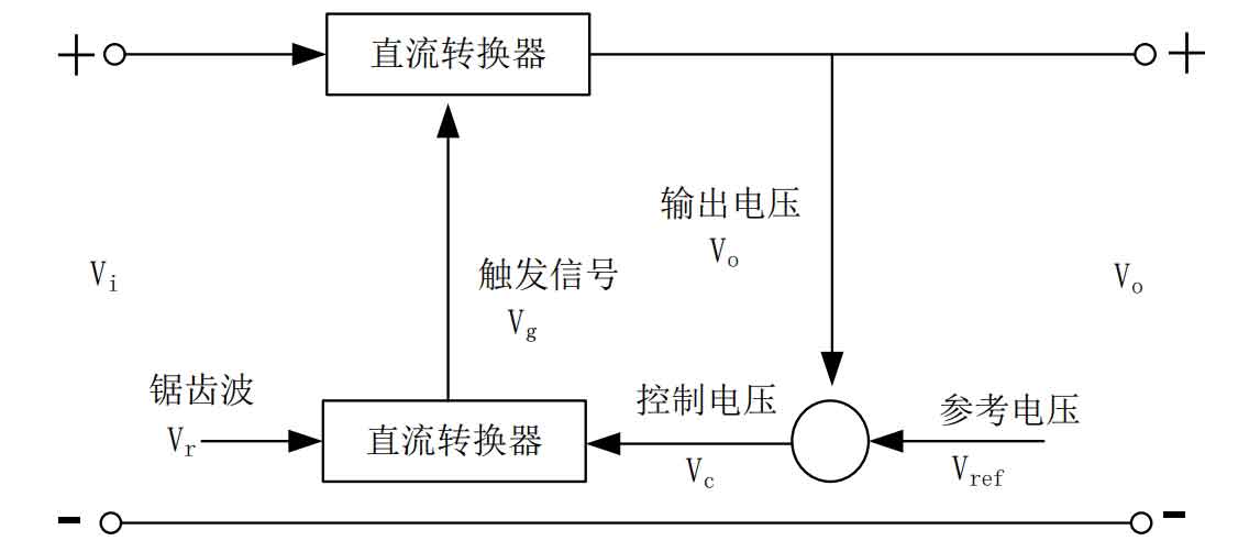
In Figure 2, the principle of generating PWM waves in a DC power converter circuit is shown. By comparing the reference signal and sawtooth wave, a modulation pulse width control switch is generated to control the conduction and turn off of the switching tube, thereby adjusting the output voltage to match the target output voltage value.

DC power converters can be divided into three types based on the application location: step-down, step-up, and step-down. In order to achieve the goals of battery boost and DC bus boost, a bidirectional boost/boost power converter is added between the photovoltaic energy storage section and the inverter section. Based on the dynamic voltage rise and fall range of the battery and DC bus, the addition of an isolation transformer is chosen to achieve both electrical isolation and DC voltage rise and fall functions, so as to match the voltage on the inverter side and energy storage side. At the same time, high-frequency isolation has small volume, high efficiency, and low cost, which can also meet the requirements of economic and practical use.
1. Analysis of buck DC power converter and boost DC power converter
The buck power converter and boost DC power converter are the basic forms of DC conversion. By comparing and analyzing them, we can guide the design of the DC boost/boost bidirectional converter in the following text.
1.1 Analysis of DC buck power converter
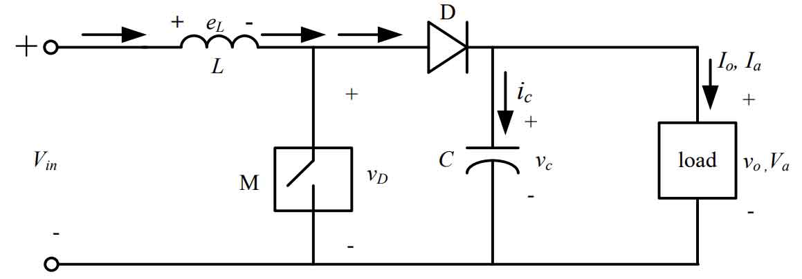
The buck power converter consists of a PWM controlled power switch, a freewheeling diode, and an output LC filtering circuit, operating in both switch on mode and diode freewheeling mode. As shown in Figure 3, adjusting the output voltage value is achieved by controlling the on/off state of the switching tube M.
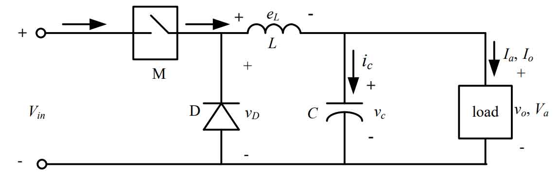
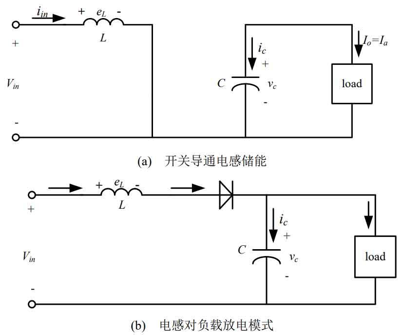
As shown in Figure 4 (a), switch M conducts the input terminal and discharges the output capacitor and load through inductor L. As shown in Figure 4 (b), when switch M is turned off, the circuit formed by the freewheeling diode and inductor continues to supply power to the output capacitor and load with the energy of the inductor.
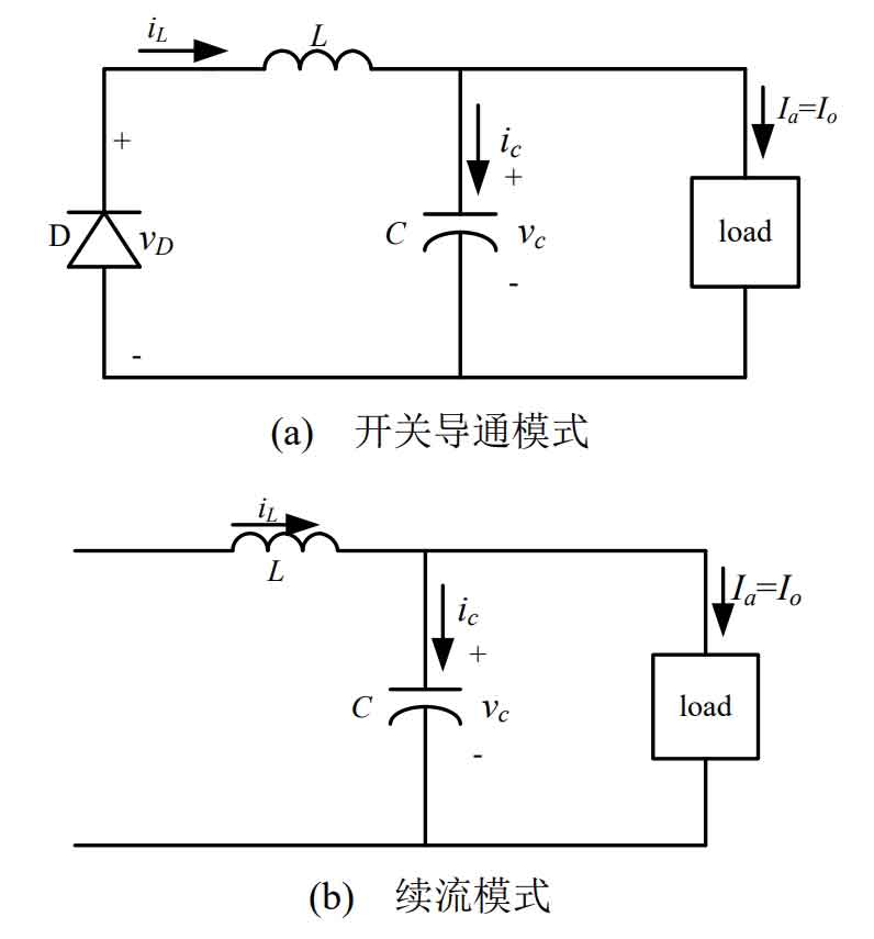
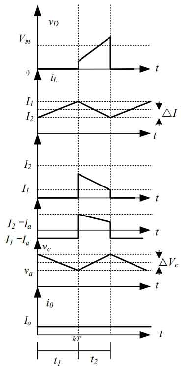
Figure 5 shows the continuous current waveform of the step-down power converter in two modes.
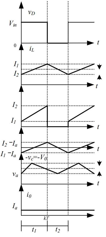
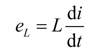
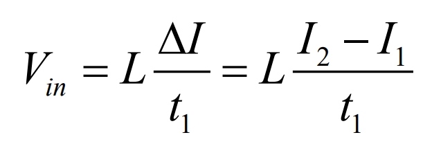
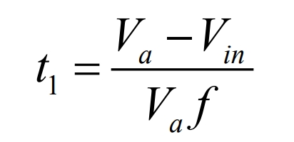
According to Figure 5, the current waveform of the step-down power converter circuit is calculated for the step-down DC circuit in two states: switch on and off. The mathematical expression for the terminal voltage of inductor L is:
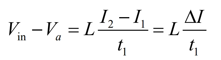
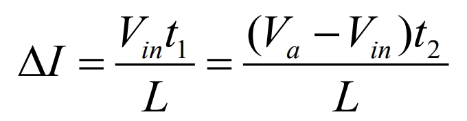
Assuming that the inductance current increases linearly from I1 to I2 within time t1:
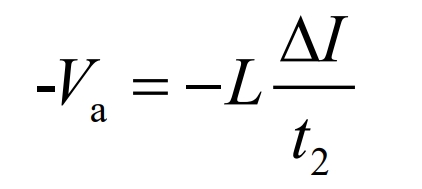
When the inductance current linearly decreases from I2 to I1 within t2 time:
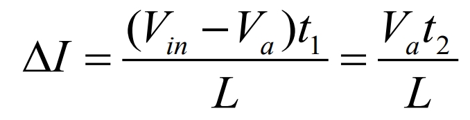
According to the formula:
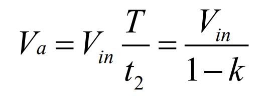
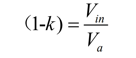
Put t1 equal to kT and t2 equal to (1-k) T into the formula and organize it to obtain the average output voltage:
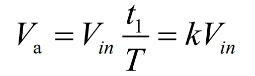
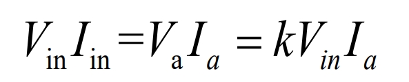
Assuming there is no loss in the circuit:
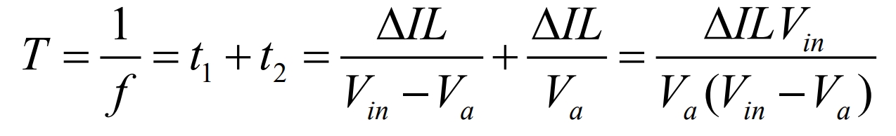
By calculating the formula, the switching period T can be obtained:
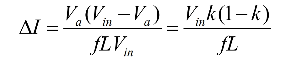
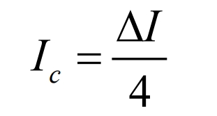
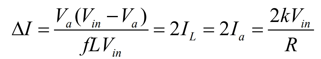
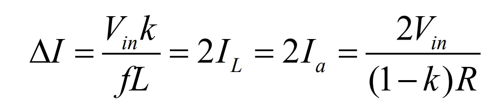
According to the formula, the peak to peak value of the ripple current is:
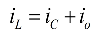
Using Kirchhoff’s current law, the inductance current Δ 𝐿 can be written as:
Assuming that the load ripple current ∆ io is small enough to be negligible, then L c ∆=∆ i i, and the average capacitive current Ic flows for a time of t1/2+t2/2=T/2:
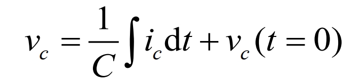
The capacitance voltage is:
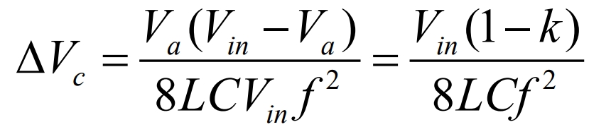
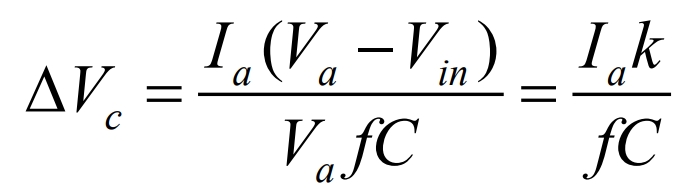
Voltage ripple peak to peak on capacitor:
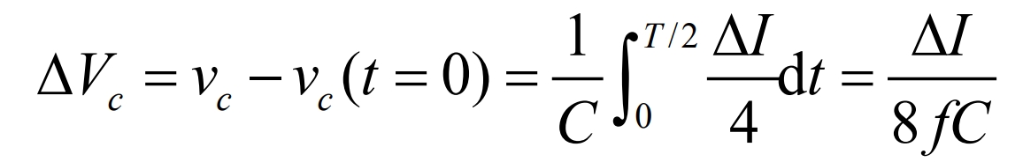
Reorganize the formula to determine the peak to peak value of capacitor ripple voltage as follows:
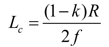
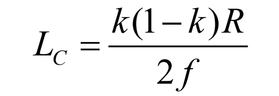
If the average value of the inductance current is IL, then the inductance ripple current 2 L ∆=I I. By organizing the formula, we can obtain:
The critical value of inductance Lc can be obtained as:
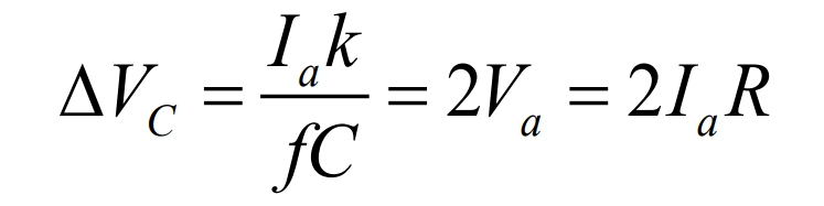
If the average value of capacitor voltage is Vc, then ∆ Vc=2Va for inductor ripple current, the following formula can be used to organize:
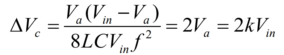
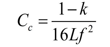
The critical value of capacitance Cc can be obtained as:
1.2 Analysis of DC Boost Power Converter
As shown in Figure 6, the boost power converter is also composed of three circuits: PWM controlled switching transistor M, freewheeling diode D, and output LC filter. There are two operating modes, including switch conduction mode and diode freewheeling mode.
The equivalent circuit of the DC boost power converter is shown in Figure 7 when the switch M is turned on and off.
When switch M is turned on, the inductor charges and stores energy. When switch M is turned off, the inductor discharges the output capacitor and load.
Figure 8 shows the current waveforms of inductor charging and power generation modes.
The transformation of inductance current in two states can be assumed that iL linearly increases from I1 to I2 through t1, and the mathematical expression of the boost circuit is:
IL decreases linearly from t2 to I1:

The formula can be used to obtain:
If t1 equals kT and t2 equals (1-k) T, the average output voltage can be obtained by substituting it into the formula:
Reorganize the formulas to obtain:
Substituting k=t1/T=t1f into the formula yields:
Assuming there is no loss in the circuit:
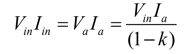
Formula organization can obtain the average input current:

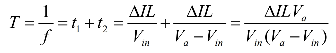
Formula organization can determine the conversion period T:
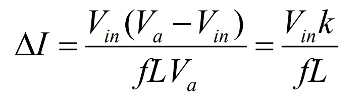
According to the formula, the peak to peak value of the ripple current is:
When the switch is turned on, the capacitor supplies the load current to t=t1 for a period of time, during which the average capacitor current is Ic=Ia, and the peak to peak value of the capacitor ripple voltage is:

By substituting the formula, the peak to peak values of the capacitor ripple voltage can be reorganized as follows:
If the average value of the inductance current is IL, then the inductance ripple current Δ 𝐼=2IL, using the formula to organize:
The formula shows that the critical value Lc of inductance is:
If the average value of the capacitor voltage is Vc, then the ripple current of the inductor is ∆ Vc=2Va, which can be obtained by substituting into the formula:
Obtain the critical capacitance value Cc:
The characteristics of the step-down and step-up power converters were mainly discussed, and it was found that this unidirectional power converter only requires one power switching element, with a simple structure and an efficiency of over 90%. The difference between the two power converters is that the conduction and freewheeling of the boost power converter start from the input end, so the input current is continuous, while the freewheeling action of the buck power converter is completed by the freewheeling part, and the input current is discontinuous. Therefore, a input filter with smoothing effect is usually needed in the buck power converter. The average output current of the boost power converter is (1-k) times smaller than the average inductance current, and the current flowing through the filtering capacitor will be larger than that coming from the step-down power converter. Therefore, the filtering capacitor and inductance of the boost power converter must be selected to be larger than the capacitance and inductance values used by the step-down power converter.
2. Design and analysis of a bidirectional DC buck power converter with isolation
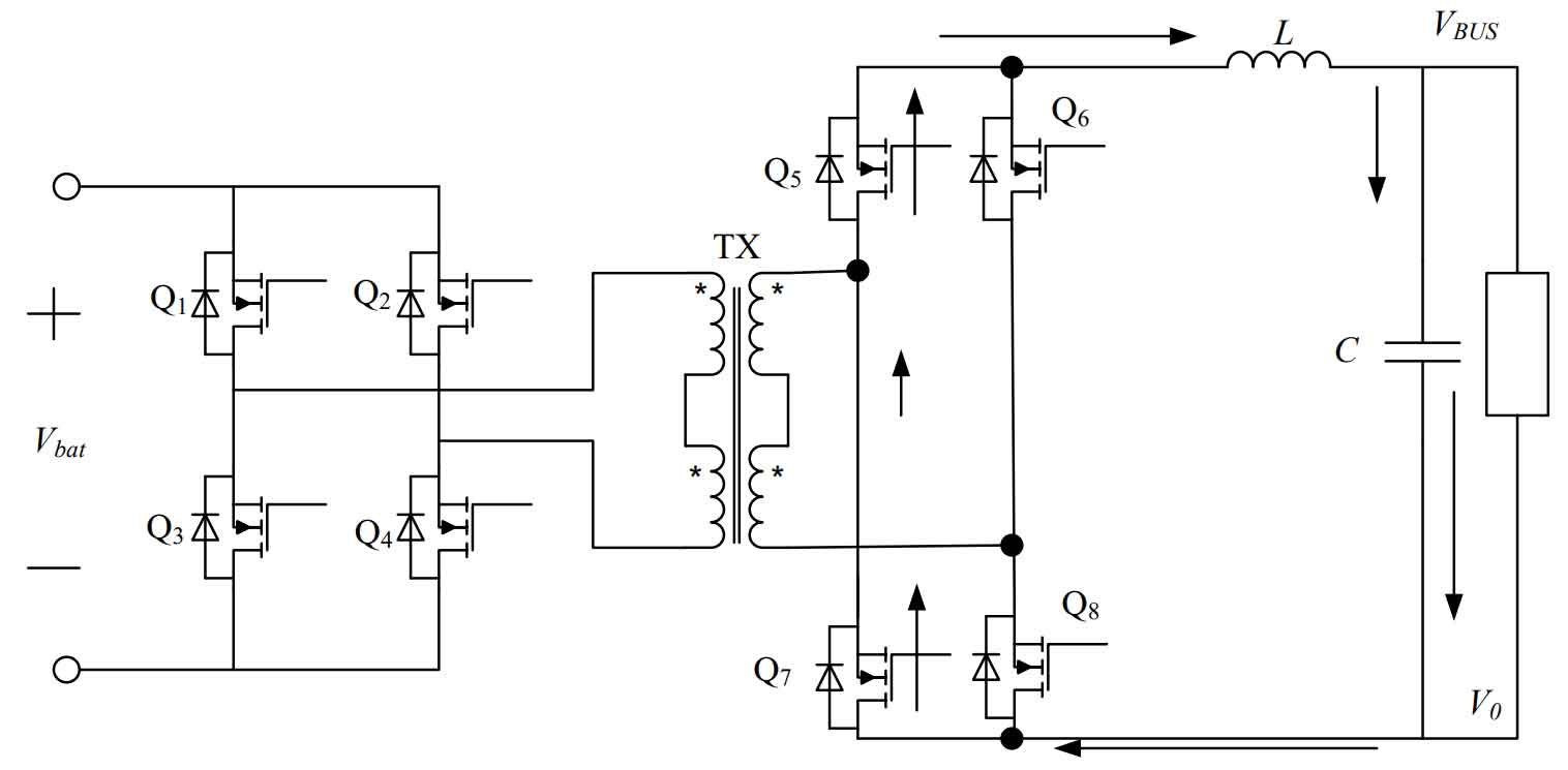
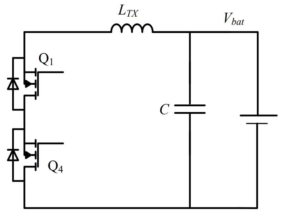
If an isolation transformer is added to both ends of the bidirectional DC power converter, it is called an isolated bidirectional DC power converter. If an isolation transformer is not required, it is called a non isolated bidirectional DC power converter. Non isolated bidirectional DC power converters are inexpensive and easy to implement, but they require compatibility with step-down and step-up functions for the same inductor, making them less suitable for high-power applications. Additionally, the range of step-down and step-down is generally limited by the inductor, resulting in a relatively narrow range. The advantage of an isolated bidirectional DC power converter is that it can adjust the voltage rise and fall ratio range by adjusting the turn ratio of the transformer’s primary and secondary sides. This design requires a battery voltage of 48 V, a DC bus voltage of 360 V, and a voltage rise and fall range exceeding 7 times. Considering the comprehensive manufacturing cost and control difficulty, a DC voltage rise and fall power converter with isolation is selected in this design. This article uses two sets of symmetrical full bridge forward circuits, high and low voltage, to achieve DC bidirectional voltage up and down conversion, as shown in Figure 9.
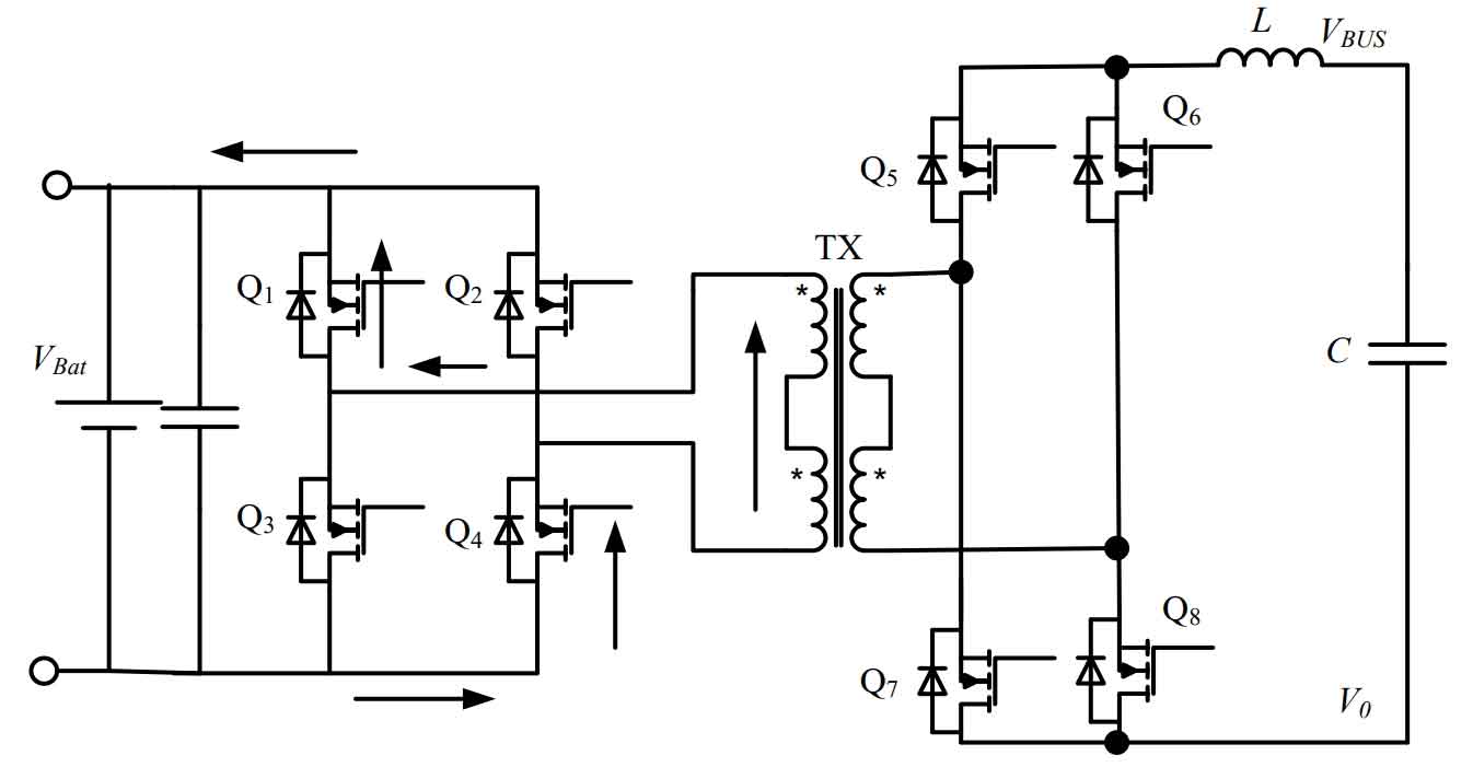
The battery side is composed of four low-voltage MOS transistors Q1, Q2, Q3, and Q4 to form a full bridge circuit, while the high-voltage DC bus side is composed of four high-voltage MOS transistors Q5, Q6, Q7, and Q8 to form another full bridge circuit; When the battery is boosted, the low-voltage side full bridge circuit forms a boost working mode with the primary side of the isolation transformer. The high-voltage side MOS is in rectification working state; When the DC bus voltage is reduced for charging, the high-voltage side front bridge circuit forms a voltage reduction working mode with the isolation transformer secondary side, and the low-voltage side MOS is in rectification working state at this time.
2.1 Design and Analysis of Forward Boost Transformation for Bidirectional DC Boost Power Converter
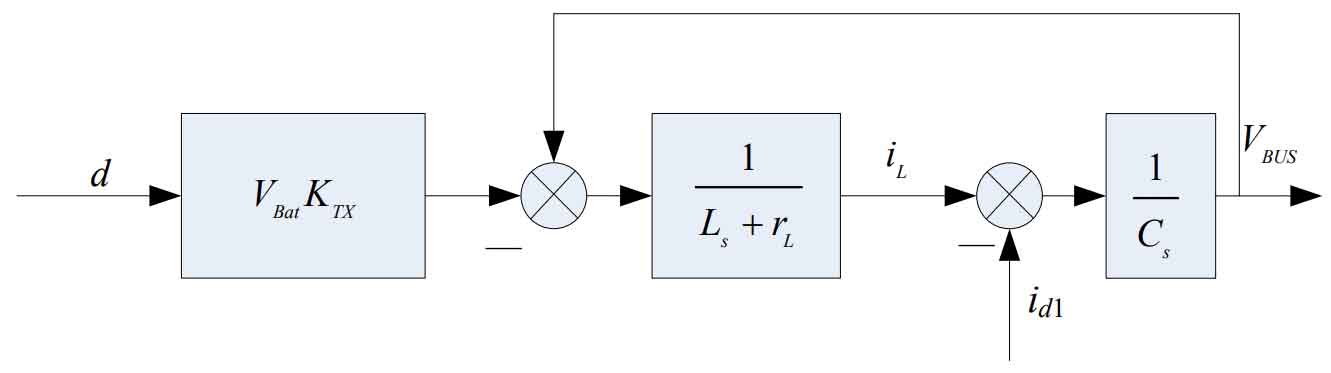
Assuming that TX is an ideal transformer in Figure 9, and the effects of magnetic saturation and leakage are ignored, the boost power converter is a typical full bridge forward circuit. According to the working principle of full bridge forward, the circuit can be equivalent to Figure 10.
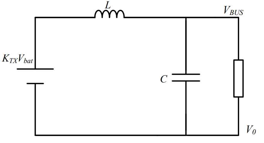
In the equivalent circuit shown in Figure 10, if there is a group of conduction in Q1, Q4, Q2, and Q3, it can be equivalent to a group of LC filtering circuits. Vbat is the voltage of the system’s energy storage battery, and KTX is the transformation ratio of the isolation transformer. At this point, the current change of inductance L directly affects the stability of the DC bus voltage, because switch tubes Q1 and Q4 are complementary to Q2 and Q3, and the conduction time is equal. The change in DC bus voltage is determined by the current load power and the conduction time of the switch tube within one switching cycle.
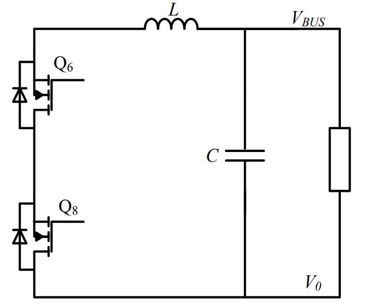
Figure 11 shows the ideal equivalent circuit when Q1 and Q4 or Q2 and Q3 are turned off simultaneously. When Q1 and Q4 are turned off simultaneously, the inductance current will continue to flow. In the ideal situation, the inductance L will continue to flow through capacitor C and MOS tubes Q6 and Q8.
In order to design a full bridge forward control system, it is necessary to establish a mathematical model of the full bridge forward circuit.
(1) Average mathematical model
In the previous section, the working situation of full bridge forward excitation in different states of the switching tube was explained. Starting from the inductance voltage, the average mathematical model of full bridge forward excitation was obtained.
Analyze the filtering inductance L of the DC bus. If the inductance current is iL and the load current is id, then for the DC bus voltage VBUS, there are:
For the voltage of the DC bus filtering inductor L, when 1 and 4 tubes or 2 and 3 tubes are turned on:
When Q1 and Q4 or Q2 and Q3 are turned off, when the circuit in Figure 12 continues to flow, there are:

Assuming 𝐷 is the duty cycle, if only the circuit in Figure 12 exists, the average voltage of the DC bus filtering inductance L within one switching cycle is:

Among them, 0 ≤ D ≤ 0.5.
In addition, the relationship between the DC bus filtering inductance L, voltage VL, and current iL is:
The average mathematical model of the full bridge forward excitation under ideal freewheeling conditions is established through calculation, as shown in Figure 13.
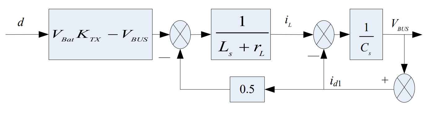
(2) Overall model
Based on the different states of the switching tubes, an average mathematical model was established. Due to the uncertainty of the model, the model was simplified and approximated. The VBUS voltage was treated as the voltage control object, and the average inductance current was treated as the current control object. The entire secondary side was equivalent to a uniform LC circuit. The overall model can be obtained as shown in Figure 14:
2.2 Design and analysis of bidirectional DC buck power converter for reverse buck conversion
Assuming that TX is an ideal transformer in Figure 9, and the effects of magnetic saturation and leakage are ignored, the step-down power converter is also a typical full bridge forward circuit. According to the working principle of full bridge forward, the circuit can be equivalent to Figure 15.
In the equivalent circuit shown in Figure 15, as long as there is a set of MOS transistors turned on in Q5, Q8, Q6, and Q7, it can be equivalent to an LC type filtering circuit. KTX is the transformation ratio of the transformer, and Vbat is the voltage of the battery. At this point, the current of the inductor LTX determines the magnitude of the charging current. The power transistors Q5 and Q8 are complementary to Q6 and Q7 in terms of conduction. During each conduction period, the opening time of the power transistor is equal, and the charging voltage change depends on the current bus voltage and the ratio of the current power transistor opening time to the closing time.
The ideal equivalent circuit when the power transistor is turned off simultaneously is shown in Figure 16. When Q5, Q8, Q6, and Q7 are turned off simultaneously, their inductors need to have a freewheeling circuit. In an ideal situation, capacitor C and MOSFET act as the freewheeling circuit for the inductors, as shown in Figure 17.

3. Summary
Elaborate on the bidirectional DC conversion process from the battery end to the DC bus end of a household solar off grid inverter energy storage system. Introduce the structure and working principle of bidirectional DC boost/boost power converter from DC buck power converter and DC boost power converter. Analyzed the mathematical model of full bridge forward DC bidirectional conversion and designed a DC voltage up and down bidirectional conversion circuit.