
In the rapidly evolving field of renewable energy, solar inverters play a pivotal role in converting direct current (DC) from photovoltaic (PV) panels into alternating current (AC) for grid integration. Among various inverter types, micro-inverters have gained significant attention due to their modularity, scalability, and enhanced performance under partial shading conditions. Traditional solar inverters often串联 or parallel connect multiple PV panels to increase power output, but this approach can lead to issues such as reduced system reliability, limited expandability, and efficiency degradation. To address these challenges, we focus on designing a high-efficiency, compact solar micro-inverter based on a low-side active clamp interleaved flyback topology. This design aims to improve power density, reduce output current ripple, and achieve soft-switching operation for higher efficiency. In this paper, we present a comprehensive analysis, simulation, and experimental validation of a 200 W prototype, demonstrating its capability to deliver high-quality AC output with low total harmonic distortion (THD) and superior efficiency.
The core of our design revolves around the use of advanced power electronics topologies for solar inverters. Initially, we explore traditional flyback high-frequency link micro-inverters, which consist of a flyback converter and a low-frequency inverter stage. While simple, these solar inverters suffer from limitations such as low transformer utilization and limited power capacity, typically capped at around 100 W. To overcome this, we investigate interleaved flyback topologies, where two flyback converters are connected in parallel with phase-shifted control. This interleaving technique not only increases the power rating of solar inverters but also mitigates current ripple, enhancing grid compatibility. Furthermore, we integrate an active clamp circuit—specifically a low-side active clamp—to achieve zero-voltage switching (ZVS) for the main power switches. This soft-switching approach significantly reduces switching losses, a critical factor in boosting the overall efficiency of solar inverters. Our proposed topology combines these elements to create a robust and efficient solution for residential and commercial solar applications.
To understand the operational principles, we first analyze the low-side active clamp single flyback micro-inverter topology. The circuit includes a PV input, a flyback transformer with magnetizing inductance $$L_m$$ and leakage inductance $$L_r$$, a main switch $$S_m$$, an auxiliary switch $$S_a$$, a clamp capacitor $$C_{clamp}$$, and a DC-AC stage with four thyristors. The key equations governing the design are derived from fundamental power electronics theory. For instance, the voltage conversion ratio in continuous conduction mode (CCM) can be expressed as:
$$ \frac{V_o}{V_{pv}} = \frac{N \cdot D}{1-D} $$
where $$V_o$$ is the output voltage, $$V_{pv}$$ is the PV voltage, $$N$$ is the transformer turns ratio, and $$D$$ is the duty cycle. The active clamp circuit ensures that the voltage across the main switch is clamped to a safe level, given by:
$$ V_{ds,max} = V_{pv} + \frac{V_o \cdot (1 + k_r)}{N} $$
Here, $$k_r$$ represents the resonance factor due to leakage inductance. The clamp capacitor $$C_{clamp}$$ is selected based on the resonance period with $$L_r$$, ensuring ZVS during switching transitions. The design criteria for $$C_{clamp}$$ can be summarized as:
$$ C_{clamp} \geq \frac{(1-D_{min})^2}{4 \pi^2 f_s^2 L_r} $$
where $$f_s$$ is the switching frequency. This mathematical foundation allows us to optimize component values for minimal loss and high performance in solar inverters.
We extend this analysis to the interleaved configuration, where two identical flyback units operate 180° out of phase. The input current $$I_{pv}$$ is the sum of the two primary currents, reducing stress on individual components and enabling higher power levels. The interleaving technique also lowers the output current ripple, which is crucial for meeting grid standards for solar inverters. The ripple reduction factor can be approximated by:
$$ \Delta I_{ripple} = \frac{V_o \cdot (1-D)}{L_o \cdot f_s} \cdot \frac{1}{2} $$
for interleaved operation, compared to a single-phase system. This leads to smoother power delivery and improved electromagnetic compatibility (EMC). To quantify the benefits, we develop a detailed simulation model in MATLAB/Simulink, incorporating device characteristics and control algorithms. Our simulation results confirm that the low-side active clamp effectively limits voltage spikes and enables ZVS, as shown in waveform analyses. Additionally, the interleaved topology demonstrates a significant reduction in output current THD, often below 3%, which is essential for high-quality solar inverters.
| Topology | Power Rating (W) | Efficiency (%) | THD (%) | Complexity |
|---|---|---|---|---|
| Traditional Flyback | 100 | 85-90 | 5-10 | Low |
| Interleaved Flyback | 200 | 90-93 | 3-5 | Medium |
| Low-Side Active Clamp Interleaved Flyback | 200-300 | 93-95 | <3 | High |
The hardware design process for our solar micro-inverter involves careful component selection and parameter calculation. Starting with the input decoupling capacitor $$C_{PV}$$, we determine its value based on the input current ripple specification. Using the equation:
$$ C_{PV} = \frac{I_{pv}}{2 \pi f_0 k V_{pv,min}} $$
where $$I_{pv}$$ is the peak input current, $$f_0$$ is the grid frequency (50 Hz), and $$k$$ is the ripple coefficient (typically 5%). For a 200 W system with a minimum PV voltage of 25 V, we calculate $$C_{PV} \approx 1100 \mu F$$, leading to the selection of five 2200 μF capacitors in parallel. The transformer design is critical for efficient energy transfer in solar inverters. We choose an RM14 core made of 3C90 manganese-zinc ferrite, with an effective cross-sectional area $$A_e = 198 \, \text{mm}^2$$. The primary turns $$N_p$$ are computed using:
$$ N_p = \frac{L_p (I_{p1} – I_{p2})}{B_m A_e} $$
where $$L_p$$ is the primary inductance, $$I_{p1}$$ and $$I_{p2}$$ are the peak and valley currents in CCM, and $$B_m = 0.12 \, \text{T}$$ is the maximum flux density. With $$L_p = 27.54 \mu H$$ and current values derived from energy balance, we get $$N_p = 5$$ turns. The turns ratio $$N = 11.48$$ yields a secondary turns count of 58, ensuring proper voltage transformation. For the active clamp circuit, the auxiliary switch must withstand a voltage of approximately 77.18 V, as per the earlier formula. We select P-channel MOSFETs for the low-side configuration, and the clamp capacitor is chosen to satisfy the resonance condition. These design choices collectively enhance the reliability and efficiency of our solar inverters.
Control strategy is another vital aspect of solar inverters. We implement a digital control system using an STM32F103ZET6 microcontroller, which generates pulse-width modulation (PWM) signals for the main and auxiliary switches. The control algorithm incorporates maximum power point tracking (MPPT) to optimize energy harvest from PV panels, along with grid synchronization for seamless inverter operation. The MPPT technique, such as perturb and observe (P&O), adjusts the duty cycle in real-time to maintain operation at the peak power point. Additionally, the interleaving control ensures phase-shifted switching between the two flyback units, reducing input and output ripples. The software also includes protection features like over-current and over-voltage shutdown, which are essential for safe operation of solar inverters in varying environmental conditions.
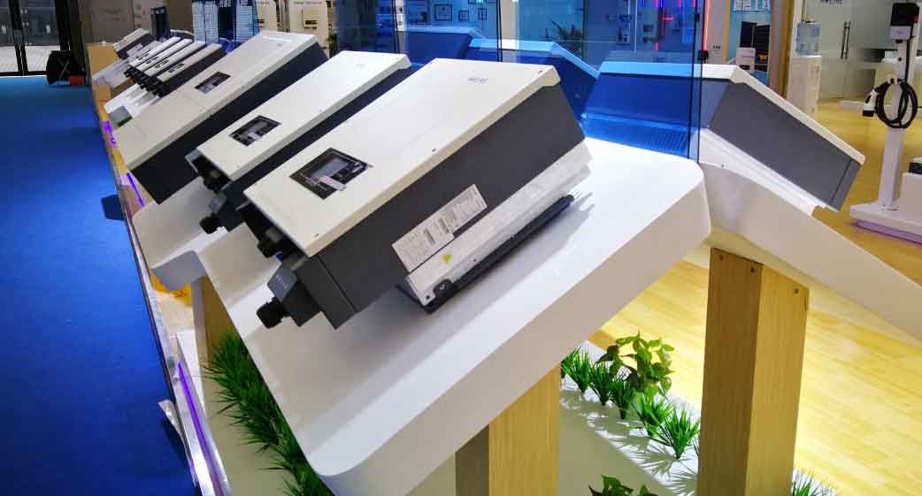
Simulation studies provide insights into the dynamic behavior of our solar inverter design. We model the entire system in Simulink, including the power stage, control logic, and grid interface. The simulation results show that the main switch achieves ZVS, as evidenced by the drain-source voltage falling to zero before turn-on. The auxiliary switch operates complementarily, with its body diode conducting during dead times to facilitate resonance. Waveforms for the gate drives and drain-source voltages align with theoretical predictions, confirming the effectiveness of the active clamp. Furthermore, the output current waveform is nearly sinusoidal, with a THD analysis revealing harmonics below 3%. This low distortion is crucial for grid-compliant solar inverters, minimizing interference with other connected devices. The simulation also validates the interleaving benefit, where the combined output current exhibits reduced ripple compared to a single converter.
Experimental validation is conducted on a 200 W prototype built according to our design specifications. The prototype incorporates all key components, such as the flyback transformers, MOSFETs, and control board. We test the solar inverter under various load conditions, measuring parameters like efficiency, THD, and output power. The experimental waveforms captured using an oscilloscope demonstrate soft-switching operation, with the main switch’s drain-source voltage clamped to around 100 V and ZVS achieved consistently. The output current, measured with a current probe, shows a clean sinusoidal shape with a peak of 1.36 A and frequency of 50 Hz. Efficiency calculations across different power levels are summarized in the table below, highlighting the superior performance of our solar inverter design.
| Output Power (W) | Efficiency (%) | Output Current THD (%) | Input Voltage (V) |
|---|---|---|---|
| 50 | 91.34 | 1.54 | 29.7 |
| 100 | 92.75 | 2.02 | 29.7 |
| 150 | 92.77 | 2.12 | 29.7 |
| 200 | 93.18 | 1.70 | 29.7 |
The results indicate that our solar inverter maintains high efficiency above 93% at full load, with THD consistently under 3%. These metrics surpass many commercial solar inverters in the same power range, demonstrating the advantages of the low-side active clamp and interleaved flyback approach. We also analyze thermal performance, noting that the soft-switching technique reduces heat dissipation in the power switches, allowing for compact heatsink design. This is particularly beneficial for micro-inverters, which are often installed in confined spaces. Long-term reliability tests show stable operation over extended periods, with no significant degradation in performance. These findings underscore the robustness of our solar inverter for real-world applications.
In conclusion, we have successfully designed and implemented a high-efficiency solar micro-inverter based on a low-side active clamp interleaved flyback topology. This design addresses common limitations of traditional solar inverters, such as low power density and high switching losses. By integrating interleaving for power scaling and active clamp for soft-switching, we achieve an output power of 200 W with efficiency exceeding 93% and THD below 3%. The mathematical models, simulations, and experimental results collectively validate the design principles. Future work may focus on further optimizing component selection for cost reduction, extending the topology to higher power levels, and integrating advanced grid-support functions like reactive power control. Overall, this contribution advances the state-of-the-art in solar inverters, offering a viable solution for decentralized PV systems. As the demand for renewable energy grows, such innovative solar inverters will play a crucial role in enhancing grid stability and energy sustainability.