
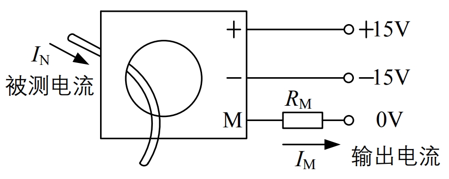
1. Block diagram of main circuit and control structure of solar grid-connected inverter experimental system
Based on the principle and output characteristics of photovoltaic cells, this chapter mainly analyzes the MPPT method, develops a mathematical model for solar inverters, designs a grid-connected control method, and verifies the correctness of its theory through MATLAB simulation.This chapter will focus on the software and hardware design of photovoltaic grid-connected inverter systems, mainly including three aspects: the hardware design of the main circuit, the hardware design of the control circuit, and the design of the control software.Figure 1 shows the main circuit and control structure diagram of the solar grid-connected inverter experimental system.
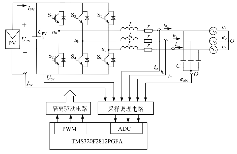
The system samples 8 signals, including the output voltage Upv, output current Ipv, three-phase inductor currents ia, ib, ic, and three-phase grid voltage eabc of the photovoltaic array.The control strategy of the system is mainly implemented through the TMS320F2812 digital signal processor of TI. The 8 signals are sampled by AD and then enter the DSP2812 for control strategy, and the output PWM signal drives the switch tube.
2. Design of key links for solar inverter grid connection
2.1 Design of grid-connected inductance experiment parameters
The AC side inductance plays an important role in the grid-connected experiment. It can isolate the grid electromotive force and the AC side voltage of the solar inverter, store energy, facilitate energy supply during freewheeling, and filter the output AC current.Moreover, as inductance is a passive device, the solar inverter can transmit reactive power to the grid.Therefore, in the experiment, the conditions and calculation process for the grid-connected inductance are as follows:
1) Meet the fast current tracking characteristics
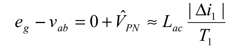
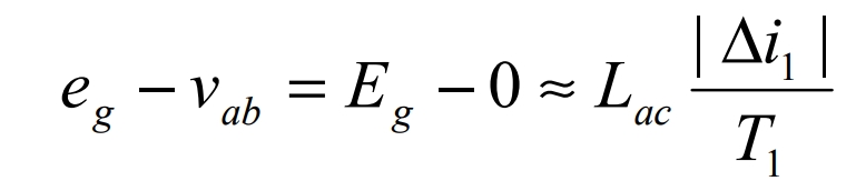
Because the grid-connected current is an AC quantity, the speed of current change must keep up with the voltage change.The rate of change of current is greatest at the zero crossing point. At this point, in order to meet the rapidity of current response, the inductance must be sufficiently small.Let’s assume a switching period Ts, and the zero crossing point is T1.
Under steady state conditions, when 10 ≤ t ≤ T, it is:
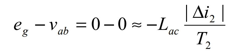
When T1 ≤ t ≤ Ts, we have:
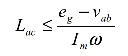
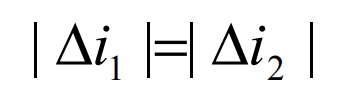
In order to meet the requirements of fast current tracking, it is necessary to:
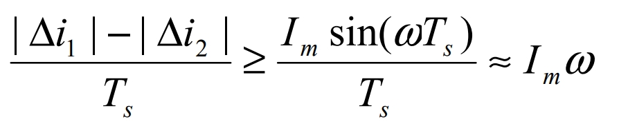
Where, |Δi1| and |Δi2| are the current changes during the T1 and T2 periods, mI is the maximum peak value of the AC current, and ω is the fundamental angular frequency of the AC current.
In summary,
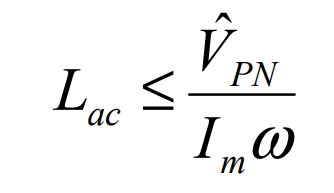
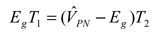
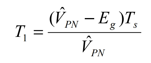
When the PWM duty cycle (T1/T2) is maximized, the fastest current tracking response should also be achieved, at which point eg − vab = ˆVPN, so:
2) The electric induction on the AC side meets the need to suppress current harmonics
The electrical induction is large enough to suppress harmonic currents, which satisfies the filtering effect.The pulsation is most severe when the harmonic current is near the peak of the sinusoidal current, so a PWM switch near the peak is analyzed.
Under steady state conditions, when 0 ≤ t ≤ T1, there is:
When T1 ≤ t ≤ Ts, we have:
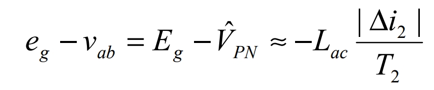
Where, Eg is the peak value of the grid electromotive force.
In steady state, near the peak of the sine wave, there is:
In summary,
Since T1 + T2 = Ts, we have:
Assuming that the maximum amplitude of harmonic current pulsation is Δimax, we can obtain:
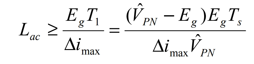
Finally, the value of the network side inductance is:
When the inductance is too large, the response speed of the entire system will be affected. Taking into account all factors, the experimental inductance is set to 5mH.It can be seen that the selection of experimental parameters for the inductance is also in line with the selection principles and circumstances of the previous simulation parameters.
2.2 Design of detection circuit
Use the Yubo module CHV-25P voltage Hall sensor and LA-50P current Hall sensor from Beijing Senshe Electronics Co., Ltd. to sample a total of 8 signals including three-phase grid voltage, photovoltaic array output voltage, three-phase grid current, and photovoltaic array output current.
1) CHV-25P Voltage Hall Sensor
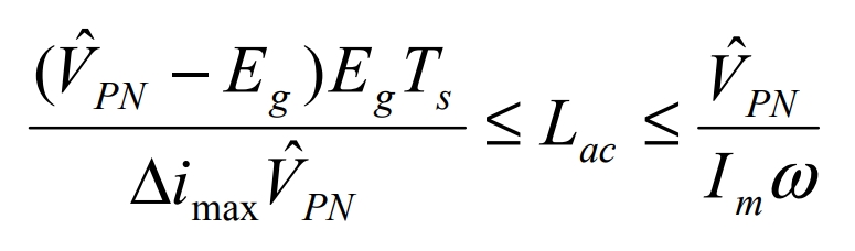
The voltage Hall sensor uses CHV-25P, which can be equivalent to a transformer with a primary-secondary ratio of 2500:1000. It samples using the principle of magnetic compensation and can isolate the main circuit and control circuit.The sensor’s rated current value on the primary side is 10mA, and its circuit connection diagram is shown in Figure 2.The sensor requires ±12V or ±15V for power supply.The voltage in the sampling circuit is input to the sensor through a current limiting resistor R1, and finally input to the sampling conditioning circuit of the DSP through a sampling resistor RM.
2) LA-50P current Hall sensor
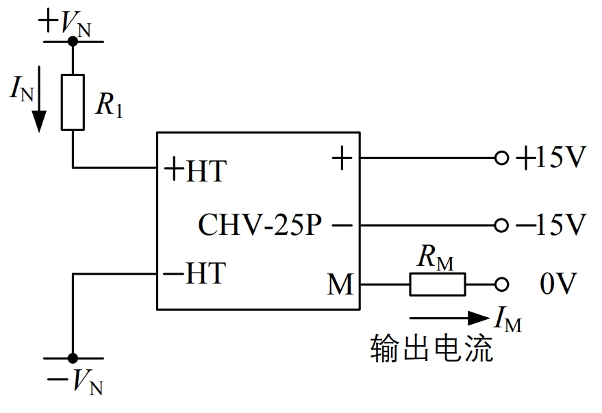
The current Hall sensor uses LA-50P, which can also be equivalently regarded as a transformer with a primary-secondary transformation ratio of 1000:1 and a rated primary current of 50A. The circuit diagram of the sensor is shown in Figure 3.The sensor senses current through electromagnetic principles and inputs it into the sampling conditioning circuit through a sampling resistor.
3. Hardware composition of control circuit
3.1 Overall composition of control circuit
The control system of solar grid-connected inverters should have strong data processing capabilities, so the requirements for software and hardware are very high. The entire control system circuit mainly consists of DSP control chips and peripheral circuits, sampling and conditioning circuits, PWM drive circuits, DA conversion circuits, etc. The control system structure diagram is shown in Figure 4.
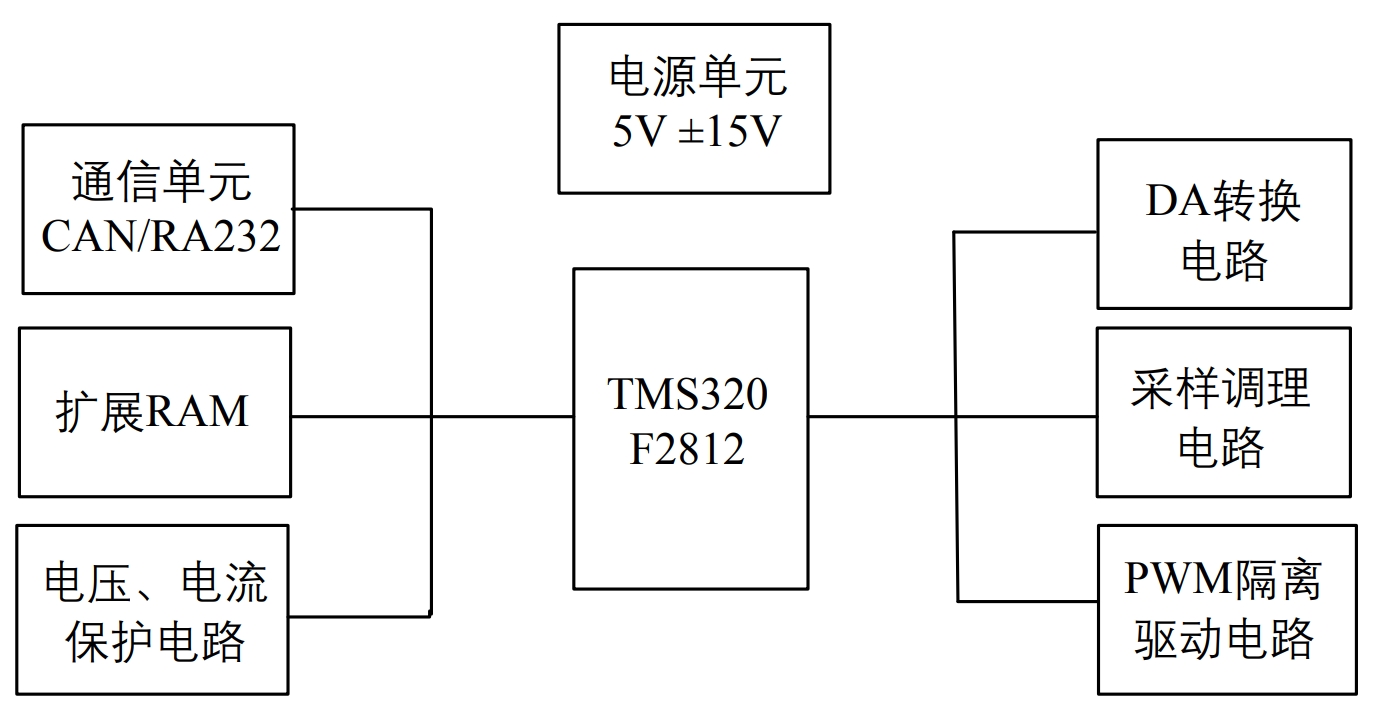
The control chip of the system uses the TMS320X2812 from the American company TI. In the experiment, the control circuit of the system includes the sampling circuit for the main circuit, the power supply circuit for the DSP, the reset circuit, the level conversion circuit, the drive circuit, and so on.
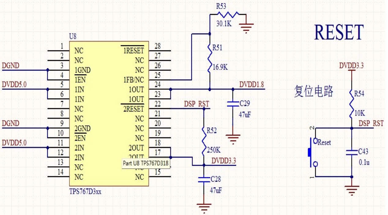
3.2 Power supply circuit and reset circuit
Using TMS320X2812 as the control chip of the system, due to the strict requirements of the power supply voltage of 2812, it requires a Flash voltage of 3.3V and a core voltage of 1.8V, so a special circuit is required to supply power to it. Figure 5 shows the power supply circuit and reset circuit of 2812.
3.3 Voltage and current sampling circuit
The control circuit needs to sample the voltage and current of the main circuit, and send the sampled voltage and current signals to the 2812 for processing. In this system, it is necessary to sample the output voltage and current of the solar panel, the BOOST output voltage, and the output current of the solar inverter. Figure 6 can collect the signals.
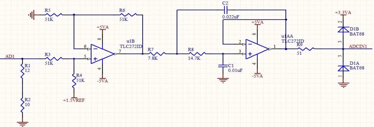
The voltage requirement for the AD sampling pin of the DSP2812 is 0-3.3V. In order to protect the DSP2812 from voltage shocks during sampling, a limiting circuit is set up after the sampling signal enters the processor. The limiting circuit mainly limits the signal through two anti-parallel diodes, which are BAT68-04W with a conduction voltage of 1.5V. Considering that the Hall output is an AC signal, an adder is used to uniformly raise the sampling voltage by 1.5V to meet the voltage requirement at the AD sampling pin.In addition, to avoid interference from stray signals on the sampling signal, a second-order filter is added between the adder and the limiting circuit to filter the sampling signal.
3.4 Switch tube drive circuit
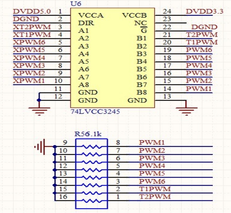
Considering the driving capability of DSP-generated signals, a level conversion chip is first required to perform level conversion on the ports to be used. Figure 7 below raises the 3.3V output from the 2812 to 5V, which is then passed through the drive circuit in Figure 8 to drive the switch transistor.
4. Control software flowchart
The control software for the solar grid-connected inverter was developed using the integrated development environment Code Composer Studio (CCS) provided by TI in the design.CCS includes a complete set of tools for developing and debugging embedded applications.It supports C language and assembly language programming, and it also has debuggers, compilers, build project environments, simulators, source code editors for each TI device series, as well as other various special functions.C language programming is flexible and convenient, with rich data types and operators, while assembly language programming is more complex and less readable, but has faster operation speed and execution efficiency.The control chip of the solar grid-connected inverter in this article is the TMS320F2812 digital signal processor from TI, which is programmed in software CCStudio v3.1 using C language.In the experiment, the connection between software and hardware is implemented using the ICETEK-5100USB 2.0 emulator provided by Beijing Ruitai Innovation Technology Co., Ltd.
4.1 Flowchart of main program
The overall flowchart of the system program.This article mainly uses the clock and control system, interrupt system, event manager, analog-to-digital conversion module ADC, etc. of the DSP2812.The following is a brief introduction to these parts of the DSP2812.
Clock and control system: To enable the DSP to perform its functions step by step, it is necessary to provide power to the DSP and continuously provide regular clock pulses to the CPU. This function is mainly implemented by the internal oscillator OSC of the DSP2812 and the clock module based on the phase-locked loop PLL.
Interrupt system: The application of interrupt signals is usually generated by software or hardware, which enables the CPU to suspend the main program being executed and execute the interrupt service routine.The interrupt system can be divided into three levels of interrupt: peripheral interrupt, PIE level interrupt, and CPU level interrupt.The interrupt flag bit in the peripheral register needs to be manually cleared, while the setting and clearing of the PIE level interrupt and CPU level interrupt flag bits are automatically completed.
Event manager: The DSP2812 has two event managers, EVA and EVB, which have exactly the same functionality.The event manager mainly implements the output of PWM signals, and one EVA or EVB can generate 8 PWM signals.
Analog-to-digital conversion module (ADC): converts analog quantities into digital quantities and provides them to the controller for use.The DSP2812 has a 12-bit resolution and is a pipeline structure.There are 16 sampling channels in the ADC module, which are divided into two groups: Group A channels ADCINA0~ADCINA7 and Group B channels ADCINB0~ADCINB7.In the main program flowchart, the system’s operation requires the following steps in order: initialization of system functions, disabling CPU interrupts, clearing CPU interrupt flags, initializing the PIE control register and interrupt PIE vector table, initializing the EV module and ADC module, enabling CPU interrupts, enabling global interrupts, enabling real-time interrupts, waiting for interrupts, etc.
4.2 Flowchart of interrupt service subroutine
When the program designed in this article runs, it will enable periodic interrupt.When a periodic interrupt occurs, the control program will run and update.Firstly, it samples the 8 signals of Upv, IpV, ea, eb, ec, ia, ib, and ic to determine whether there is overvoltage or overcurrent in the circuit. If there is an overvoltage or overcurrent, it means that the circuit is not working properly and the pulse should be blocked.If the voltage and current work properly, then the MPPT program can be executed.Then, the phase-locked loop, power feedforward control, and current loop control are executed in turn, and finally the interrupt is enabled.
5. Experimental verification
5.1 Independent operation of solar inverter
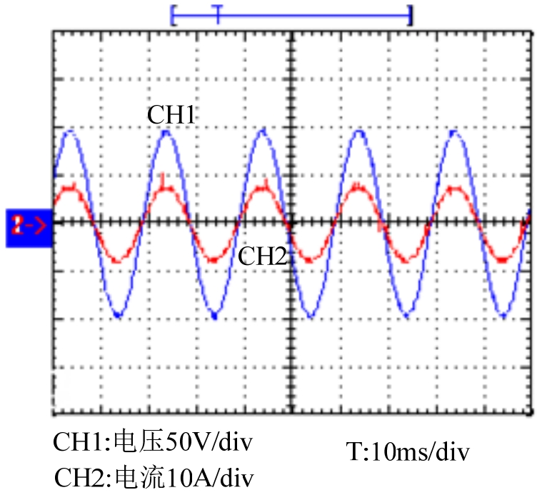
Firstly, the normal operation of a single solar inverter was achieved. The steady-state experimental waveform of the current closed loop is shown in Figure 9. In the experiment, the three-phase load was 20Ω, CH1 was the load voltage waveform, the probe of CH1 (the blue part in Figure 9) measured the voltage as 50V/div, CH2 was the load current waveform (the red part in Figure 9), and the probe of CH2 measured the current as 10A/div.The oscilloscope recorded the test time as 10ms/div.It can be seen from the figure that the test voltage and current waveforms are very good.
5.2 Phase-locked loop experiment
In order to determine the state of the power grid, solar photovoltaic solar grid-connected inverters should continuously detect the power grid to ensure the normal operation of the solar inverter.Usually, phase-locked loop technology is used to detect the power grid, which provides phase information of the grid voltage for control to ensure that the grid current and grid voltage are in phase and in the same frequency during grid-connected operation.
The Phase Locked loop (PLL) is essentially an automatic feedback control system that completely synchronizes the phase between the output signal and the input signal. It feeds back the phase signal.In this experiment, the software phase-locked method is used to lock the system.
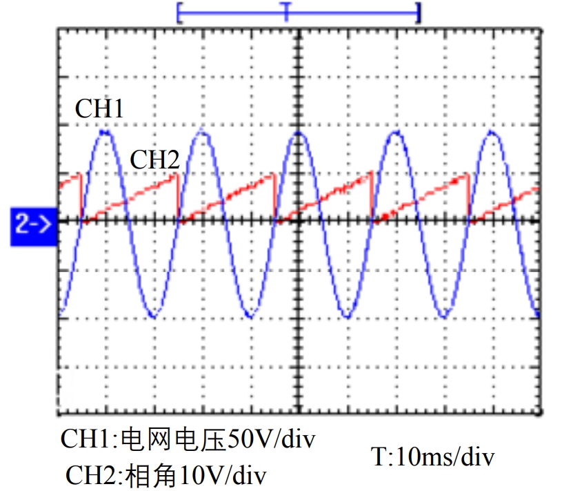
Figure 10 shows the experimental waveform diagram using a software phase-locked loop, where the sine wave is the voltage of the grid phase a and the sawtooth wave is the phase of the grid phase a. It can be seen from the diagram that the output phase of the phase-locked loop can fully track the phase of the grid voltage.
5.3 Grid connection experiment
Based on the above experimental foundation, the grid-connected experiment was verified. The DC side input voltage was 500V, the grid-connected voltage peak-to-peak value was 400V, and the grid-connected current was 5A. The experimental waveform diagram is shown below.
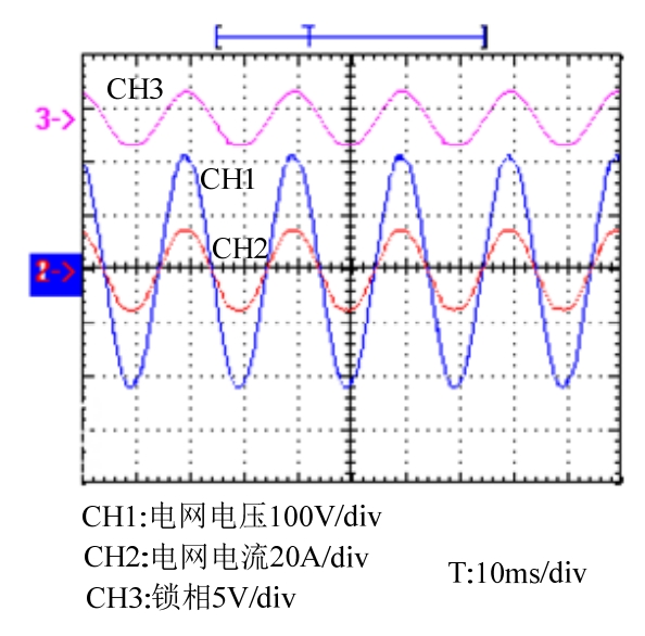
Figure 11 shows the steady-state operation waveform of the grid-connected experiment.As can be seen from the figure, the quality of the grid-connected startup waveform is good, and the grid-connected current can quickly reach the same frequency and phase of the grid voltage. The grid-connected process has little impact on the grid, and there is no distortion at the zero crossing point.
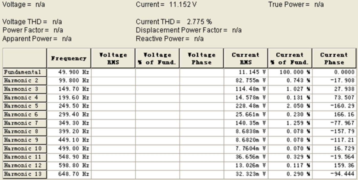
The THD analysis of the grid-connected current is shown in Figure 12. It can be seen that the THD of the grid-connected current is 2.775%, which is less than 5%, meeting the grid-connection standard requirements.
6. Summary
The main power hardware and control circuit hardware of the experimental platform, as well as the flowchart of the control software are introduced.Firstly, the overall structural diagram of the system is given. Secondly, the key components of the main circuit and control, such as the filtering inductor, the drive circuit, and the sampling circuit, are designed. The flowchart of the main program of the system and the flowchart of the interrupt service subroutine are also designed.Finally, experimental verification is carried out, and the experimental waveforms of single solar inverter independent control, phase-locked loop, and solar inverter grid-connected are given. It can be seen that the theoretical analysis and design are feasible and effective.
Faced with the problems facing social development such as energy shortage and environmental degradation, in order to achieve future development, we should focus on researching the application of photovoltaic grid-connected technology to obtain more mature and stable technological achievements.This article mainly studies and analyzes the two-stage three-phase photovoltaic grid-connected system, and systematically conducts theoretical calculation analysis and application research on the characteristics of photovoltaic cells, MPPT algorithms, model establishment, and current control algorithms for three-phase solar grid-connected inverters.The work and achievements made for this design are summarized as follows:
1) Based on the physical model of the photovoltaic cell, the mathematical model of the photovoltaic array is derived, and the photovoltaic array simulation model is constructed on the Simulink module of Matlab.The simulation circuit is built, and the output characteristics of the photovoltaic cell are studied through the output waveform. The photovoltaic output characteristic curves under different light intensities and different temperatures are simulated.Based on the photovoltaic cell simulation model, the method and principle of maximum power point tracking are proposed, and several common MPPT methods are introduced. The application of disturbance observation method using Matlab/Simulink is simulated with emphasis.
2) A simulation model for MPPT of photovoltaic power generation system with Boost circuit as the core was established. The working principle of Boost circuit was analyzed, and on this basis, the algorithm was simulated using Matlab/Simulink in combination with disturbance observation method.The mathematical model of three-phase solar grid-connected inverter was derived, and the current feedforward decoupling control strategy was designed. The control method was selected based on the current feedforward decoupling double-loop control method, and a simulation model was constructed to verify the correctness of the control strategy.
3) The software and hardware design of the photovoltaic grid-connected inverter system, mainly including the design of the main circuit hardware, control circuit hardware and control software.The solar inverter independent operation experiment, phase-locked loop experiment and grid-connected experiment were conducted, and the experimental data obtained can achieve the expected goals.It can be seen that the selection of topics and theoretical analysis are correct and effective, and the three-phase grid-connected inverter with MPPT in solar power generation has certain application prospects in the field of solar power generation.In the future work, we will conduct more in-depth research on the photovoltaic grid-connected power generation system, and continue to explore more stable, reliable and rapid photovoltaic power generation grid-connected control strategies.There are still many technical problems in the field of photovoltaic power generation, especially in the tracking of the maximum power point, which needs to be developed in order to maximize the efficiency of solar power generation.Although there is still a big gap between China and foreign advanced levels in the technical level and production process of photovoltaic power generation, I firmly believe that with the unremitting efforts of Chinese scientific and technological personnel, the gap will be shortened soon, and high-performance and high-quality solar grid-connected inverters will be brought to the market and achieve independent industrialization.