
1. Introduction and Background
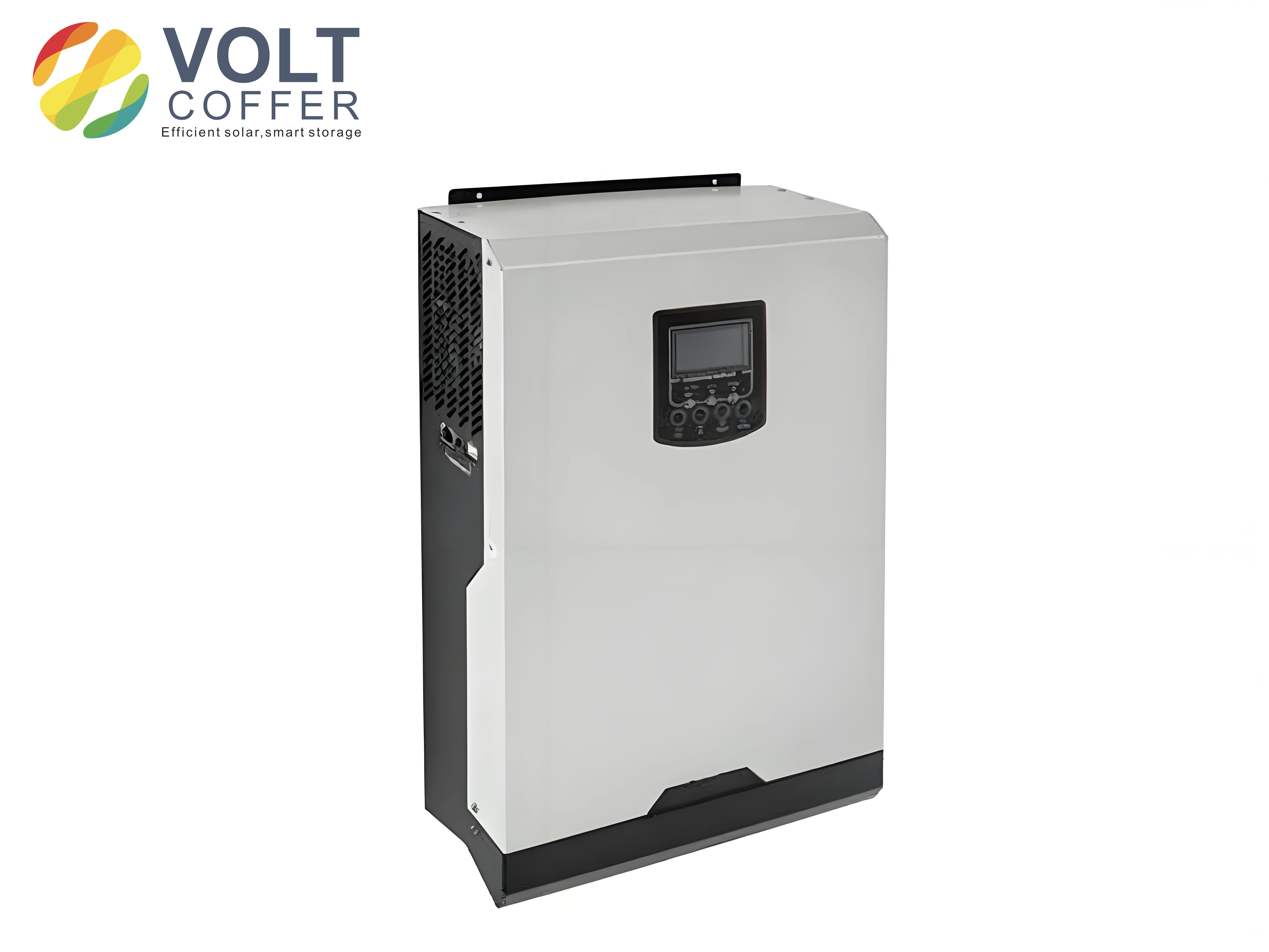
Modern society is confronted with the dual challenges of depleting traditional energy reserves and escalating environmental pollution. Solar energy, because of its clean nature, broad availability, and renewability, has emerged as one of the most promising alternatives. Photovoltaic (PV) power generation is now recognized as a viable way to convert solar energy directly into electricity. In my research, I focused on the fact that the solar inverter is the central component that connects the photovoltaic panels to the electrical grid. Therefore, developing an efficient data acquisition system for solar inverters is essential for improving the reliability and performance of PV power stations.
Traditional data acquisition systems for PV stations often suffer from inconsistent communication protocols, a lack of network connectivity, and their large physical dimensions. These shortcomings increase development complexity, weaken remote-management capabilities, and limit the applicability of such systems. To overcome these problems, I designed a compact and intelligent data acquisition system based on the MODBUS-RTU protocol. This system collects real-time data from solar inverters and transmits the data to a distributed PV operation-management platform, thus providing necessary support for operation, maintenance, and performance optimization.
2. System Design and Key Technologies
2.1 Overall System Architecture
My proposed system can be divided into two main parts: the lower computer (data acquisition terminal) and the upper computer (monitoring platform). The lower computer is centered on an STM32F103C8T6 microcontroller. It communicates with solar inverters through an RS485 serial bus using the MODBUS-RTU protocol. A 4G wireless module is used to connect the data acquisition system to the Internet, so that the collected information can be uploaded to the distributed PV operation-management platform through the TCP/IP protocol. This design enables remote monitoring and control of multiple solar inverters from a central station.
| Aspect | Traditional Data Acquisition System | My Designed System |
|---|---|---|
| Communication protocol | Proprietary or inconsistent | Standard MODBUS-RTU |
| Network capability | No remote access | 4G wireless TCP/IP |
| Size | Large and bulky | Compact embedded design |
| Intelligence | Low | Remote configuration and diagnostics |
| Scalability | Limited | Can connect multiple solar inverters |
2.2 MODBUS Communication Protocol
The MODBUS protocol is a well-established industrial communication standard that operates on a master-slave architecture. In my system, the data acquisition terminal acts as the master, and each solar inverter acts as a slave. The protocol uses a request-response mechanism. The master sends a query frame containing the slave address, function code, register address, and CRC check; the addressed slave then replies with the requested data. I selected the RTU (Remote Terminal Unit) transmission mode for this project because it provides higher data density and better efficiency compared to ASCII mode.
The general MODBUS frame structure is shown below:
$$ \text{ADU} = \text{Slave Address} + \text{PDU} + \text{Error Check} $$
where the Protocol Data Unit (PDU) is:
$$ \text{PDU} = \text{Function Code} + \text{Data} $$
In MODBUS-RTU mode, a frame is separated by an idle interval of at least 3.5 character times. The CRC (Cyclic Redundancy Check) is a 16-bit checksum calculated over the frame content. The CRC algorithm is implemented as follows:
$$ \text{CRC16} = ( \text{CRC16} \oplus \text{byte} ) \times \text{poly} $$
where the polynomial for MODBUS is \( 0xA001 \). I implemented the CRC calculation using a lookup table and verified it with every received query or response.
2.3 Selection of Serial Communication Interface
Two commonly used serial interfaces are RS232 and RS485. Since solar inverters are often installed in remote outdoor locations, robust and long-distance communication is necessary. I compared the key characteristics and selected RS485 for the following reasons.
| Parameter | RS232 | RS485 |
|---|---|---|
| Transmission distance | About 15 meters | Up to 1000 meters |
| Communication direction | Full duplex | Half duplex |
| Logic levels | +3 V to +15 V for logic 0; -3 V to -15 V for logic 1 | +2 V to +6 V for logic 0; -6 V to -2 V for logic 1 |
| Number of nodes | 1 transmitter, 1 receiver | Up to 32 nodes |
| Interference immunity | Low | High (differential signaling) |
I used an SP3485 chip as the RS485 transceiver. The RE and DE pins of the SP3485 are connected together, allowing a single GPIO on the STM32F103C8T6 to control whether the transceiver is in transmit mode or receive mode. When the combined pin is low, the transceiver is in receive mode; when high, in transmit mode. This simple configuration is ideal for half-duplex MODBUS communication.
2.4 Upper Computer Software
For testing and verification, I used two software tools on the PC side: SSCOM serial assistant and MODBUS SLAVE debugger. SSCOM can display and transmit data in both hexadecimal and ASCII modes, and it also supports periodic sending. MODBUS SLAVE simulates a MODBUS slave device, allowing me to assign register values that emulate the measurement points of a solar inverter. This tool proved extremely helpful for verifying the correctness of my communication protocol and data processing routines.
3. Hardware Circuit Design
3.1 Selection of the Main Controller
I compared two popular ARM Cortex-M3 microcontrollers: the STM32F103C8T6 from STMicroelectronics and the GD32F103C8T6 from GigaDevice. The table below summarizes their main specifications.
| Parameter | STM32F103C8T6 | GD32F103C8T6 |
|---|---|---|
| Core | ARM Cortex-M3 | ARM Cortex-M3 |
| Word length | 32-bit | 32-bit |
| Supply voltage | 2.0 V to 3.6 V | 2.6 V to 3.6 V |
| SRAM | 64 KB | 96 KB |
| Flash | 128 KB | 3 MB |
| GPIO pins | 37 | 37 |
| ADC channels | 18 | 16 |
| PWM channels | 15 | 8 |
| Unit price (approx.) | USD 1.1 | USD 2.5 |
I selected the STM32F103C8T6 because of its lower power consumption, extensive documentation, rich peripheral library, and cost-effectiveness. The development board that I used integrates the STM32F103C8T6 chip with an RS485 interface, an LED indicator, an ADC input, a 4G module socket, and a Mini-USB power interface. This board provided all the necessary hardware for my data acquisition system.
3.2 STM32F103C8T6 Minimum System
The minimum system includes the MCU, power supply circuitry, clock source, reset circuitry, and program download/debug interface. I used an 8 MHz crystal oscillator as the high-speed clock and a 32.768 kHz crystal as the low-speed clock for the real-time clock. The reset circuit uses an RC network to keep the MCU in reset state until the power supply is stable. Power is supplied at 5 V through the USB port, and an on-board voltage regulator converts it to 3.3 V for the MCU and peripherals.
The download and debug circuit uses the SWD (Serial Wire Debug) protocol. The SWD interface requires only two connections: SWDIO and SWCLK, which simplifies wiring compared with JTAG. I used a J-Link debugger to flash the firmware and to perform real-time debugging in Keil μVision4.
3.3 RS485 Serial Communication Module
The RS485 circuit is built around an SP3485 transceiver. The A and B differential lines are connected to the solar inverter’s RS485 bus through a screw terminal. Two PTC resettable fuses (SMD1812) protect against overcurrent and short circuits. The pin connections are listed below.
| SP3485 Pin | Function | Connected to |
|---|---|---|
| RO | Receiver output | STM32 USART RX |
| DI | Driver input | STM32 USART TX |
| RE | Receiver enable (active low) | STM32 GPIO |
| DE | Driver enable (active high) | STM32 GPIO |
| A | Non-inverting bus terminal | RS485 A line |
| B | Inverting bus terminal | RS485 B line |
Because the MODBUS-RTU protocol uses half-duplex communication, I connected the RE and DE pins together on the board. The STM32 GPIO then switches the SP3485 between receive and transmit states. The default state is receive, and the firmware changes the pin to transmit only when a frame is about to be sent.
3.4 4G Wireless Communication Module
To enable remote monitoring and over-the-air firmware updates, I integrated a Quectel EC200S-CN 4G module into the system. The EC200S-CN supports LTE-TDD/LTE-FDD, WCDMA, and GSM networks. It offers maximum download speeds of 10 Mbps and upload speeds of 5 Mbps, which is more than sufficient for the small amount of measurement data from solar inverters. The module has a built-in TCP/IP stack, so the STM32 can open a TCP connection to the server using simple AT commands.
The process of connecting the EC200S-CN module to a remote TCP server involves three major AT commands:
AT+QICSGP=1,1,"CTNET","","",1AT+QIACT=1AT+QIOPEN=1,0,"TCP","180.97.81.180",55131,0,2
After these commands are executed successfully, the module enters transparent transmission mode. Any data sent from the MCU through the UART is forwarded to the server, and any data received from the server is passed back to the MCU. I found that the 4G module greatly improved the practicality of the system by eliminating the need for a wired Ethernet connection in remote PV stations.
4. Software Design
4.1 Development Environment
I developed all firmware in C language using Keil μVision4, which provides integrated compilation, debugging, and flash download capabilities. I used the STM32 standard peripheral library, which makes it easier to configure the clock, GPIO, USART, ADC, DMA, and timer modules. The J-Link debugger allowed me to set breakpoints and examine variables in real time, which significantly accelerated the development and testing process.
4.2 Main Program Flow
The main program is responsible for initializing the hardware and starting the communication threads. The pseudo-code below describes the initialization steps:
1. Initialize the LED GPIO.
2. Initialize the USART for RS485 communication with 9600 baud, 8 data bits, 1 stop bit, no parity.
3. Initialize the timer for MODBUS timing.
4. Initialize the ADC and DMA.
5. Initialize the 4G module and establish the TCP connection.
6. Enter the main loop and wait for MODBUS requests.
The main loop continuously toggles the RUN LED with a 1-second delay. When the 4G module has established a network connection, the LINK LED also turns on and blinks with a 2-second period. In the main loop, the firmware checks whether a MODBUS frame has been received on the RS485 interface. If so, it validates the CRC and processes the query.
4.3 Voltage Signal Acquisition Subroutine
The STM32 has multiple ADC channels. I used one channel to measure an analog voltage signal from a sensor or a test point on the solar inverter board. To avoid consuming CPU time during data transfers, I used the DMA controller. When the ADC conversion completes, the DMA writes the result into a memory buffer without interfering with the CPU’s normal operations. The DMA configuration includes the peripheral base address (ADC data register), the memory base address, the buffer size, and the transfer direction (peripheral-to-memory).
The relationship between the raw ADC value and the actual voltage is:
$$ V_{\text{actual}} = \frac{V_{\text{ref}}}{2^n – 1} \times \text{adc\_value} $$
where \( V_{\text{ref}} \) is 3.3 V and \( n = 12 \) because the STM32F103C8T6 has a 12-bit ADC. Thus, the voltage resolution is:
$$ \Delta V = \frac{3.3}{4095} \approx 0.8058 \text{ mV} $$
This high resolution is suitable for capturing small variations in the output voltage of solar inverters. After acquiring the voltage value, the firmware stores it in a global data structure and makes it accessible to the MODBUS data mapping module.
4.4 MODBUS-RTU Communication Subroutine
My implementation of the MODBUS-RTU communication subroutine followed the standard frame format:
| Field | Length | Description |
|---|---|---|
| Slave address | 1 byte | Unique ID of the solar inverter |
| Function code | 1 byte | For example, 0x03 (read holding registers), 0x04 (read input registers) |
| Register address | 2 bytes | Starting register address (high byte first) |
| Register quantity | 2 bytes | Number of registers to read |
| CRC | 2 bytes | Low byte first |
The CRC16 calculation implemented in my code is shown below:
$$ \text{CRC} = ((\text{CRC} \gg 8) \oplus \text{byte}) \oplus \text{tbl}[\text{CRC} \& 0xFF] $$
where the lookup table is generated from the polynomial \( 0xA001 \). In the transmit function, I first copy the slave address into the command array, then calculate the CRC over the first six bytes, and finally append the lower and upper bytes of the CRC to the frame.
When the system receives a frame, the RTOS-based serial interrupt stores the received bytes in a ring buffer. When an idle interval longer than 3.5 character times is detected, the UART signals a frame completion. The application then extracts the slave address from the first byte and compares it with the configured address. If it matches, the CRC is checked. If the CRC passes, the function code and register address are examined, and the appropriate response is generated.
5. System Testing and Results
5.1 Test Environment
I tested the data acquisition system in a laboratory environment before deploying it in a real PV station. The test setup consisted of:
- STM32F103C8T6 development board with RS485 and 4G modules.
- A USB-to-RS485 converter connected to the PC.
- SSCOM serial assistant for viewing raw MODBUS frames.
- MODBUS SLAVE debugger for simulating the register map of a solar inverter.
- A distributed PV operation-management platform for remote data verification.
The serial parameters were set to 9600 baud, 8 data bits, no parity, and 1 stop bit, as required by the simulated solar inverter communication protocol.
5.2 Power Module Test
When the data acquisition system was powered through a PC USB port, the RUN LED began to blink at a frequency of approximately 1 Hz. This confirmed that the STM32 was running the main loop correctly and that the power supply circuit was stable.
5.3 4G Module Network Test
After inserting a SIM card and connecting the antenna, the LINK LED on the 4G module started blinking with a 2-second period. This indicated that the module had successfully registered with the cellular network and established a data connection. Additionally, the status was verified through the distributed PV operation-management platform, which showed the device as ‘online’ based on its serial number.
5.4 RS485 Communication Test
I connected the RS485 A and B terminals of the development board to the USB-to-RS485 converter. After opening MODBUS SLAVE and selecting the correct COM port, the software successfully displayed the connection. This confirmed that the SP3485 transceiver and the UART configuration were working correctly.
5.5 Complete System Test
I simulated a Sungrow medium-power grid-connected solar inverter using MODBUS SLAVE. The measured points included phase voltages, phase currents, active power, daily generated energy, cumulative generated energy, and PV string currents. The register addresses were configured in the firmware according to the protocol specification. For example, the daily generated energy was stored in register 5115 (0x13FB). With the offset of 1 required by the protocol, I used register 5113 in the MODBUS frame.
When the data acquisition system sent a query frame, MODBUS SLAVE responded with the appropriate data. The received response frame was captured with SSCOM and then parsed manually to verify the data. An example of the request/response pair for the daily generated energy is:
$$ \text{Request: } 01 \, 04 \, 13 \, 88 \, 00 \, 08 \, 75 \, 62 $$
$$ \text{Response: } 01 \, 04 \, 10 \, 00 \, 00 \, 00 \, 00 \, 00 \, 00 \, 64 \, 00 \, 00 \, 00 \, 3D \, CD \, 48 \, 00 \, 00 \, 1C \, 91 $$
From the response frame, I extracted the two bytes corresponding to the daily generated energy: \( 0x00 \, 0x64 \), which equals 100 in decimal. This matched the value set in MODBUS SLAVE. For the active power, which was a 32-bit floating-point value, the four bytes \( 0x40 \, 0xD4 \, 0xAC \, 0x08 \) were converted using the IEEE 754 standard:
$$ 0x40D4AC08 \approx 6.6468 \times 10^3 \ \text{W} $$
This also matched the simulated value. The same verification process was repeated for all other test points.
| Measurement Parameter | Data Format | Register Address | Simulated Value | Decoded Value | Status |
|---|---|---|---|---|---|
| A-phase voltage | 16-bit unsigned | 5001 | 240 V | 240 V | OK |
| A-phase current | 16-bit signed | 5011 | 10.5 A | 10.5 A | OK |
| Total active power | 32-bit float | 5031 | 6.6468 kW | 6.6468 kW | OK |
| Grid frequency | 16-bit unsigned | 5033 | 50.00 Hz | 50.00 Hz | OK |
| Daily generated energy | 16-bit unsigned | 5115 | 100 kWh | 100 kWh | OK |
| Cumulative generated energy | 32-bit unsigned | 5119 | 12345 kWh | 12345 kWh | OK |
| PV string 1 current | 16-bit signed | 7013 | 8.2 A | 8.2 A | OK |
After the MODBUS SLAVE tests passed, I uploaded the same data to the distributed PV operation-management platform. The platform displayed all the measured values in real time, and the readings matched the values set in MODBUS SLAVE. In addition, the platform allowed me to issue remote configuration commands, such as changing the data collection interval or restarting the data acquisition terminal. This functionality proved the practicality of my system for distant PV power plants where manual intervention is difficult.
6. Conclusion and Future Work
In this work, I successfully designed and implemented a photovoltaic inverter data acquisition system based on the MODBUS-RTU protocol. The system uses an STM32F103C8T6 microcontroller, an RS485 transceiver, and a 4G wireless module to collect measurement data from solar inverters and transmit it to a distributed PV operation-management platform. The hardware design was carefully developed to ensure stable, long-distance communication, and the software was written in C with a modular approach that simplifies future upgrades.
Extensive testing with simulated solar inverters confirmed that the data acquisition system correctly reads 16-bit integer, 32-bit integer, and 32-bit floating-point values from MODBUS registers. The CRC16 error-checking mechanism effectively detects corrupted frames, and the 4G network connection provides reliable remote access.
Although the system meets the current project requirements, I have identified several areas for future improvement:
- Improve the accuracy of the voltage signal acquisition circuit by using a higher-resolution ADC or adding external reference voltage filtering.
- Enhance the temperature and humidity resilience of the enclosure to withstand harsh outdoor environments where solar inverters are typically installed.
- Add automatic firmware version matching so that the data acquisition system can adapt to different communication protocol revisions of solar inverters without manual parameter adjustment.
- Increase the total number of connectable solar inverters by expanding the flash memory and adding more dynamic memory management.
In conclusion, my data acquisition system demonstrates improved accuracy, remote-management capability, and compactness compared to traditional designs. It provides a solid foundation for future smart monitoring and predictive maintenance of solar inverters in distributed solar power plants.