
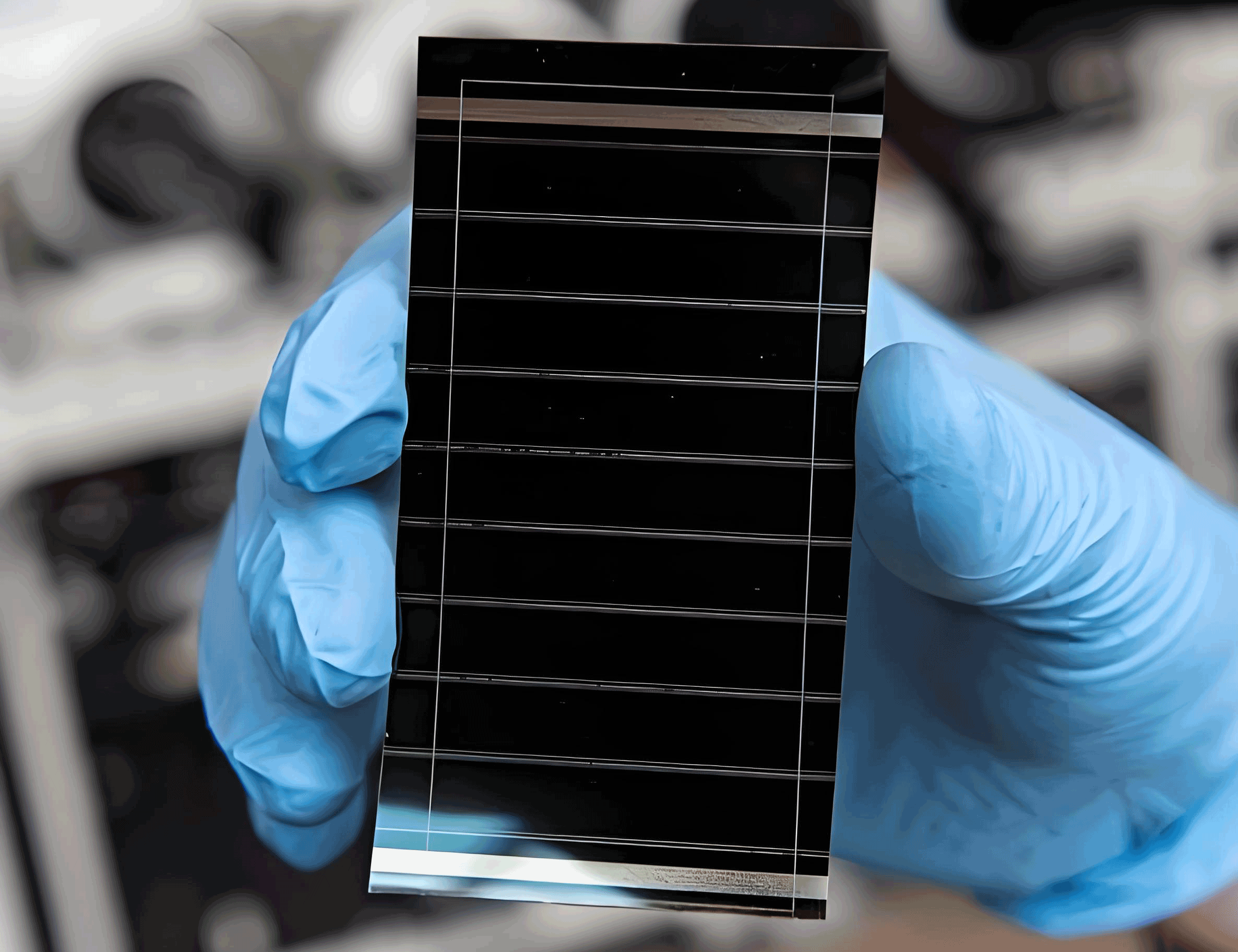
Perovskite solar cells have emerged as a promising photovoltaic technology due to their high efficiency and low-cost fabrication potential. Since their inception in 2009, they have rapidly evolved, with certified power conversion efficiencies (PCE) now exceeding 26% for single-junction devices. The two primary architectures, n-i-p and p-i-n structures, differ in the order of charge transport layers relative to the perovskite light-absorbing layer. In this article, we compare and analyze the performance enhancement strategies employed in champion efficiency devices for both structures from 2017 to 2023. By examining these strategies, we aim to provide insights into the evolution of perovskite solar cell technology and guide future developments.
The n-i-p structure typically involves an electron transport layer (ETL) deposited first on the substrate, followed by the perovskite layer and a hole transport layer (HTL). In contrast, the p-i-n structure starts with an HTL, then the perovskite layer, and an ETL. These configurations influence charge extraction, recombination losses, and overall device performance. Over the years, researchers have implemented various strategies to improve key parameters such as short-circuit current density (Jsc), open-circuit voltage (Voc), and fill factor (FF), which collectively determine PCE. The PCE is defined as:
$$ \text{PCE} = \frac{J_{\text{sc}} \times V_{\text{oc}} \times \text{FF}}{P_{\text{in}}} $$
where Pin is the incident light power density (typically 100 mW/cm² under standard test conditions). The fill factor represents the ratio of maximum power output to the product of Jsc and Voc:
$$ \text{FF} = \frac{J_{\text{mp}} \times V_{\text{mp}}}{J_{\text{sc}} \times V_{\text{oc}}} $$
Here, Jmp and Vmp are the current density and voltage at the maximum power point, respectively. Optimizing these parameters requires addressing issues like non-radiative recombination, charge transport losses, and interfacial defects.
The development of champion efficiency perovskite solar cells has seen significant progress, with n-i-p structures generally leading in PCE until recent years when p-i-n devices caught up. For instance, in 2023, a p-i-n perovskite solar cell achieved a certified PCE of 25.8%, matching that of an n-i-p device. This convergence highlights the effectiveness of advanced strategies in both architectures. Below, we summarize the performance parameters and strategies for n-i-p and p-i-n perovskite solar cells from 2017 to 2023, using tables to provide a clear overview.
For n-i-p perovskite solar cells, the champion devices have employed strategies focused on defect passivation, interface modification, and transport layer optimization. These approaches have led to incremental improvements in Jsc, Voc, and FF. A key observation is that strategies targeting the perovskite bulk often enhance Jsc, while interface treatments boost Voc. However, introducing passivation layers can sometimes reduce FF due to increased series resistance. The following table outlines the performance parameters and strategies for n-i-p perovskite solar cells over the years.
| Year | Jsc (mA/cm²) | Voc (V) | FF (%) | PCE (%) | Performance Enhancement Strategy |
|---|---|---|---|---|---|
| 2017 | 24.97 | 1.105 | 80.3 | 22.13 | Using additives to passivate defects in the perovskite layer |
| 2018 | 24.93 | 1.127 | 80.5 | 22.60 | Designing HTL with better energy-level alignment |
| 2019 | 24.92 | 1.144 | 79.6 | 22.67 | Modifying the interface between perovskite and HTL |
| 2019 | 25.24 | 1.179 | 78.4 | 23.32 | Passivating defects on the perovskite surface |
| 2019 | 26.09 | 1.150 | 79.0 | 23.73 | Using additives to improve the photoactive phase |
| 2020 | 26.18 | 1.181 | 79.6 | 24.64 | Designing HTL with higher mobility and better energy-level match |
| 2021 | 25.14 | 1.181 | 84.8 | 25.17 | Improving ETL to reduce defects and block hole carriers |
| 2021 | 26.25 | 1.174 | 81.8 | 25.21 | Using additives to passivate defects in the perovskite bulk |
| 2021 | 25.74 | 1.189 | 83.2 | 25.49 | Modifying the interface between perovskite and ETL |
| 2022 | 26.18 | 1.182 | 82.6 | 25.56 | Using additives to passivate defects in the perovskite layer |
| 2023 | 25.80 | 1.179 | 84.6 | 25.73 | Using additives to improve the photoactive phase and enhance FF |
In n-i-p perovskite solar cells, strategies involving additive-based defect passivation in the perovskite layer consistently improve Jsc by reducing non-radiative recombination and enhancing charge carrier lifetime. For example, the use of formamidinium lead iodide (FAPbI3) with additives like MDACl2 or FAHCOO has led to higher Jsc values by stabilizing the photoactive phase and minimizing defects. The Voc improvements are often linked to interface modifications, such as introducing thin layers between the perovskite and transport layers to align energy levels and reduce recombination. The ideal factor (n) in the diode equation influences Voc and FF:
$$ V_{\text{oc}} = \frac{n k T}{q} \ln\left(\frac{J_{\text{sc}}}{J_0} + 1\right) $$
where k is Boltzmann’s constant, T is temperature, q is electron charge, and J0 is the reverse saturation current density. Strategies that lower n and J0 through defect passivation result in higher Voc. However, FF can be compromised by series resistance (Rs) and shunt resistance (Rsh), as described by:
$$ \text{FF} = \text{FF}_0 \left(1 – \frac{R_s}{V_{\text{oc}}/J_{\text{sc}}}\right) \left(1 – \frac{V_{\text{oc}}/J_{\text{sc}}}{R_{\text{sh}}}\right) $$
where FF0 is the ideal fill factor. ETL optimizations, such as using SnO2 instead of TiO2, have proven effective in reducing Rs and improving FF, as seen in the 2021 champion device with an FF of 84.8%.
For p-i-n perovskite solar cells, the strategies have evolved to address challenges like inefficient electron extraction due to the p-type character of the perovskite surface when grown on HTLs. Champion devices have employed surface passivation, interface modification, and bulk perovskite engineering to enhance performance. The following table summarizes the key parameters and strategies for p-i-n perovskite solar cells.
| Year | Jsc (mA/cm²) | Voc (V) | FF (%) | PCE (%) | Performance Enhancement Strategy |
|---|---|---|---|---|---|
| 2017 | 22.99 | 1.131 | 79.1 | 20.59 | Passivating defects on the perovskite surface |
| 2018 | 21.86 | 1.175 | 81.4 | 20.90 | Modifying the interface between perovskite and ETL |
| 2019 | 23.86 | 1.143 | 82.0 | 22.34 | Using additives to improve crystal orientation |
| 2020 | 24.68 | 1.164 | 79.2 | 22.75 | Passivating defects on the perovskite surface |
| 2022 | 25.24 | 1.143 | 81.3 | 23.47 | Modifying the interface between perovskite and ETL |
| 2022 | 25.59 | 1.179 | 80.6 | 24.30 | Modifying the interface to enhance charge transport |
| 2022 | 26.10 | 1.160 | 83.8 | 25.37 | Modifying the interface to improve Jsc and FF |
| 2023 | 25.03 | 1.203 | 82.7 | 24.90 | Improving contact between perovskite and HTL |
| 2023 | 26.51 | 1.153 | 84.5 | 25.81 | Using additives to improve perovskite homogeneity |
In p-i-n perovskite solar cells, a common strategy involves modifying the perovskite-ETL interface to induce an n-type surface band structure, facilitating electron extraction. This is achieved by depositing thin layers of materials like guanidinium bromide or sulfided compounds, which passivate surface defects and shift the Fermi level. The surface band bending can be described by the Schottky barrier height:
$$ \phi_B = \chi – \psi_S $$
where χ is the electron affinity of the perovskite and ψS is the surface potential. By reducing φB, these modifications enhance Voc and Jsc. Additionally, strategies focusing on perovskite bulk homogeneity, such as using octylammonium ligands or 1-(phenylsulfonyl)pyrrole, improve FF by reducing grain boundaries and enhancing charge transport. The recent champion p-i-n perovskite solar cell achieved a high FF of 84.5% through such homogeneity engineering.
Comparing the strategies longitudinally, we observe that early approaches for both n-i-p and p-i-n perovskite solar cells relied heavily on surface defect passivation, which boosted Voc but often at the cost of Jsc and FF due to the introduction of resistive layers. Over time, the focus shifted to bulk perovskite optimization and interface engineering, leading to balanced improvements in all parameters. For n-i-p structures, the transition from TiO2 to SnO2 ETLs reduced hysteresis and improved FF, while for p-i-n structures, the development of conductive interface layers enabled better electron extraction without sacrificing Voc.
Transversely, n-i-p perovskite solar cells have benefited from advancements in HTL materials like Spiro-OMeTAD and its derivatives, which offer better energy-level alignment and higher hole mobility. In contrast, p-i-n devices often use PTAA or self-assembled monolayers as HTLs, combined with C60/BCP as ETLs, to achieve similar performance. The convergence in PCE between the two structures in 2023 underscores the effectiveness of tailored strategies for each architecture. The non-radiative recombination loss, quantified by the Voc deficit, has been minimized through these strategies:
$$ \Delta V_{\text{oc}} = \frac{kT}{q} \ln\left(\frac{1}{\text{EQE}_{\text{EL}}}\right) $$
where EQEEL is the electroluminescence external quantum efficiency. By improving EQEEL via defect passivation, both n-i-p and p-i-n perovskite solar cells have achieved Voc values close to the radiative limit.
In conclusion, the evolution of performance enhancement strategies for perovskite solar cells has been marked by a shift from simple defect passivation to sophisticated interface and bulk engineering. For n-i-p structures, optimizing the perovskite layer and ETL/HTL interfaces has led to steady improvements in Jsc and FF, while for p-i-n structures, surface band modification and homogeneity control have been key to boosting Voc and FF. The continued innovation in materials and processing techniques promises further advances in perovskite solar cell efficiency and stability. As research progresses, we anticipate that these strategies will pave the way for commercial applications of perovskite solar cells, contributing to sustainable energy solutions.