
In modern renewable energy systems, the solar inverter plays a central role in converting photovoltaic power into grid-compatible AC electricity. As the penetration of solar energy grows, electromagnetic compatibility (EMC) has become a critical design constraint. The fast switching actions of power semiconductor devices inside a solar inverter generate severe conducted electromagnetic interference (EMI), especially in the common-mode (CM) domain. This paper presents a comprehensive study on the diagnosis, modeling, and suppression of common-mode conducted EMI in high-power photovoltaic systems. We focus on a grid-connected solar inverter that integrates a Boost converter, a three-level active neutral-point-clamped (3L-ANPC) inverter, and auxiliary power supplies based on dual-switch flyback converters. Through systematic EMI measurements, multi-source diagnosis, precise CM equivalent circuit modeling, and innovative suppression techniques, we demonstrate significant improvements in the EMC performance of the solar inverter.
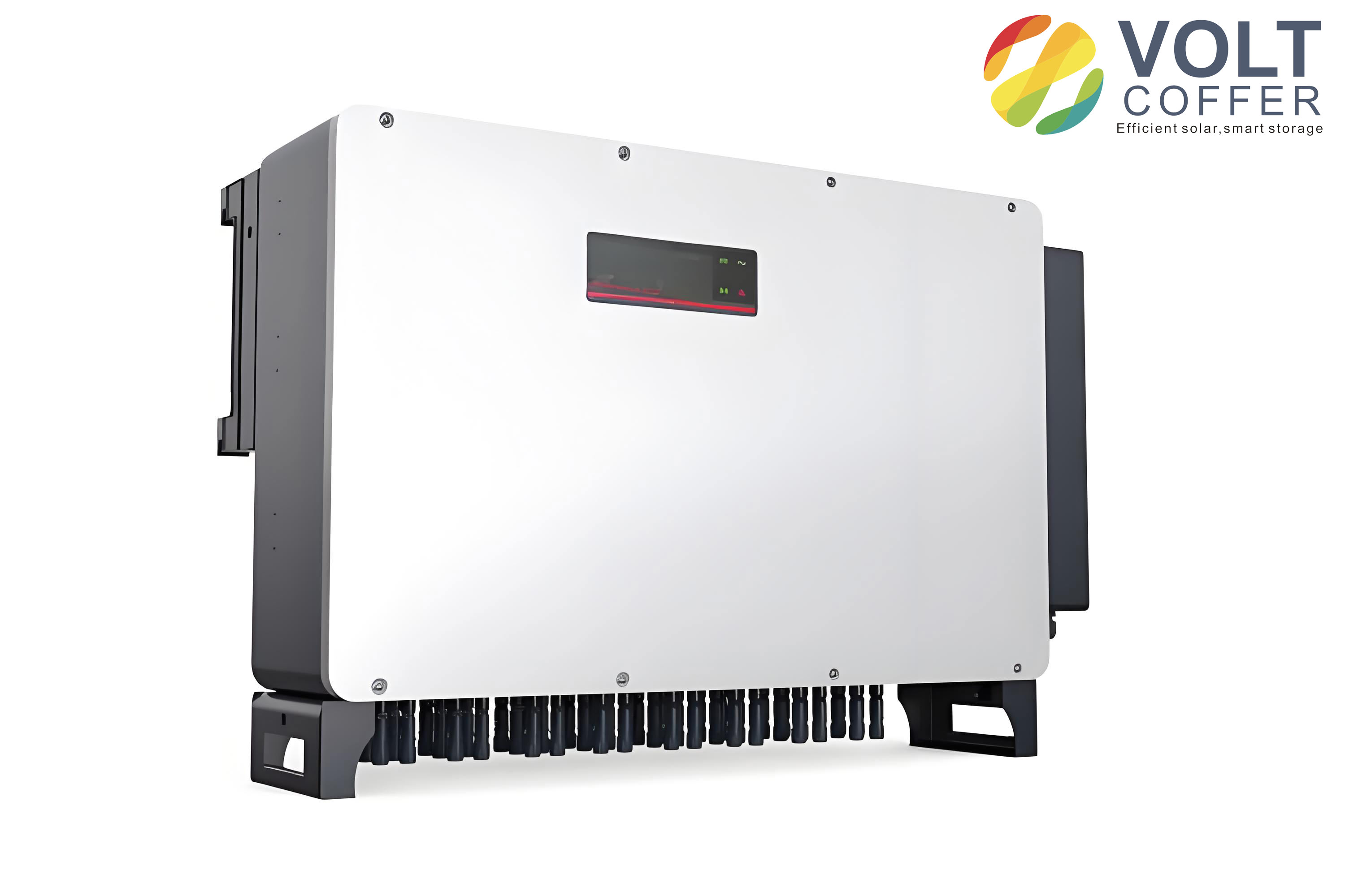
The primary goal of this investigation is to establish a complete framework for CM conducted EMI analysis in a solar inverter. The work is organized into several logical steps. First, we build a standardized EMI test platform and perform a multi-source diagnostic to identify the dominant noise sources. Second, we analyze the hidden CM propagation paths that bypass conventional filters. Third, we develop accurate frequency-domain CM models for the main power stage (3L-ANPC inverter) and for the auxiliary power supply. Finally, we propose two effective suppression methods: a balanced-bridge strategy for simultaneous AC/DC CM noise reduction, and a cancellation-capacitor technique for the flyback converter. The effectiveness of these methods is validated through both simulation and experiment.
The solar inverter under study consists of several sub-converters operating at different switching frequencies. The Boost converter raises the photovoltaic array voltage to a stable DC bus. The 3L-ANPC inverter converts the DC bus voltage into three-phase AC power. Two auxiliary power supplies provide isolated voltages for control circuits: one is fed from the DC bus and the other from the AC side. All these converters contribute to EMI, but their contributions vary with frequency. In order to diagnose the dominant sources, we performed high-resolution spectral measurements on the AC and DC ports. The switching frequencies of the main sources are listed in Table 1.
| Source | Switching Frequency |
|---|---|
| 3L-ANPC inverter | 20.5 kHz |
| Boost converter | 18 kHz |
| DC auxiliary flyback | 93.5 kHz |
| AC auxiliary flyback | 66 kHz |
To identify which source dominates a particular frequency band, we compared the spacing of spectral peaks at the AC and DC ports with the switching harmonic intervals of each source. The diagnostic results, summarized in Table 2, reveal that the 3L-ANPC inverter and the DC auxiliary power supply are the two main contributors in most bands. This finding guides the subsequent modeling and suppression efforts.
| Port | Band | Dominant Source |
|---|---|---|
| AC side | 150 kHz – 500 kHz | 3L-ANPC |
| 500 kHz – 10 MHz | DC auxiliary supply | |
| 10 MHz – 30 MHz | 3L-ANPC | |
| DC side | 150 kHz – 800 kHz | 3L-ANPC |
| 800 kHz – 10 MHz | DC auxiliary supply | |
| 10 MHz – 30 MHz | 3L-ANPC |
After identifying the dominant sources, we investigated the CM propagation paths. The solar inverter contains several parasitic capacitances between circuit nodes and ground. In particular, the auxiliary power supply’s secondary grounds are connected to protective earth through Y capacitors. We also discovered two hidden paths that bypass the designed CM filters. One hidden path exists between the auxiliary ground AGND and the grid side GRID through the parasitic capacitance of a surge arrester. The other hidden path is between AGND and the PV side through the parasitic capacitance of a current sensor. These hidden paths were confirmed by impedance measurements and significantly affect the overall CM EMI behavior. Figure 1 (not referenced) illustrates the complete CM interference path model that we derived.
EMI Modeling of the 3L-ANPC Inverter
The 3L-ANPC inverter is a key component of the solar inverter. Unlike a two-level inverter, each phase leg of the 3L-ANPC has three voltage transition nodes: A, A1, and A2. Therefore, the CM noise source cannot be represented by a single voltage source in the original circuit. We applied the substitution theorem and the superposition principle to simplify the equivalent model. For phase A, the six switches are replaced by voltage or current sources depending on their operating state. After shorting the DC bus capacitors and merging the three phases, the CM source model can be derived.
Let the phase-to-neutral voltages be defined as \(v_{AN}\), \(v_{BN}\), and \(v_{CN}\). The total CM voltage source is:
\[
v_{CM} = \frac{v_{AN}+v_{BN}+v_{CN}}{3}
\]
Similarly, the intermediate node voltages contribute:
\[
v_{CM1} = \frac{v_{A1N}+v_{B1N}+v_{C1N}}{3}
\]
\[
v_{CM2} = \frac{v_{A2N}+v_{B2N}+v_{C2N}}{3}
\]
Through analysis of the DPWM1 modulation strategy, we found that \(v_{CM1}\) and \(v_{CM2}\) are small-signal equivalents at low frequency and can be combined. The main high-frequency CM noise is generated by \(v_{CM}\) due to the switching action of the SiC devices. The resulting simplified CM equivalent circuit is shown in Fig. 2 (not included). In this circuit, the parasitic capacitances from the power module to ground are represented by \(C_{P1}\) and \(C_{P2}\), where:
\[
C_{P1} = 3 C_{S3G}
\]
\[
C_{P2} = 3 ( C_{S1G} + C_{S2G} + C_{S4G} + C_{S5G} + C_{S6G} )
\]
We measured the actual parasitic capacitances of the IGBT module using an impedance analyzer. The results are summarized in Table 3. These values were used to parameterize the model.
| Parasitic Capacitance | Value |
|---|---|
| CS1G | 77.7 pF |
| CS2G | 164.5 pF |
| CS3G | 115.3 pF |
| CS4G | 125.0 pF |
| CS5G | 22.8 pF |
| CS6G | 83.9 pF |
The passive components, such as the AC filter inductor \(L_{AC}\) and the capacitor \(C_{AC}\), were also characterized at high frequencies. The inductor was fitted by a multi-stage RLC network. The measured impedance curves show four resonances, so a four-stage model was used. The capacitor was modeled by a series RLC circuit. These high-frequency models are essential to accurately predict the CM noise spectrum.
Using the derived CM model, we performed frequency-domain simulations in CST Studio Suite. The actual CM voltage source waveform was measured with a high-voltage differential probe and transformed to the frequency domain via FFT. The simulated CM interference currents at both AC and DC ports were compared with measurements. The results show excellent agreement within the conducted EMI band, confirming the accuracy of the 3L-ANPC CM model.
Balanced-Bridge Strategy for AC/DC CM Noise Suppression
In order to reduce the CM noise generated by the 3L-ANPC inverter, we investigated two conventional balanced-bridge approaches: the AC-side balanced bridge and the DC-side balanced bridge. Both methods rely on connecting the AC filter neutral point O to a specific point on the DC side, and adding a bus-to-ground capacitor to balance the bridge impedances.
The fundamental balance condition for the bridge network is given by the impedance ratio:
\[
\frac{Z_1}{Z_3} = \frac{Z_2}{Z_4}
\]
where \(Z_1\), \(Z_2\), \(Z_3\), and \(Z_4\) are the equivalent impedances of the four branches. When this condition is satisfied, the potential difference between the inverter’s equivalent output point and ground becomes zero, thereby suppressing the CM current through the LISN.
For the AC-side balanced bridge, we connected the neutral point O to the midpoint N of the DC bus and inserted a bus capacitor \(C_{BUS}\) between N and ground. The optimal value of \(C_{BUS}\) is determined by:
\[
C_{BUS} = \frac{C_{P1}}{3} \cdot \frac{Z(L_{AC})}{Z(L_N)} – C_{P2}
\]
Our measurements gave \(C_{BUS} \approx 127.9\ \text{nF}\). This value effectively balances the bridge in the low-frequency band where the ANPC interference is dominant. The AC-side CM noise was significantly reduced; however, the DC-side suppression was not as strong because it relied on the high capacitance value rather than on the balance itself.
For the DC-side balanced bridge, we connected the neutral point O to the left side Q of the DC common-mode choke \(L_{DC-CM}\). The balance condition required increasing the connecting line inductance \(L_Q\). Although this method effectively suppressed DC-side CM noise, it adversely increased the AC-side CM noise in certain frequency bands because the total CM loop impedance was raised. Thus, neither of the two individual methods could simultaneously suppress both AC and DC CM noise without side effects.
To overcome this limitation, we proposed a coordinated AC/DC CM noise suppression strategy. The idea is to connect the neutral point O simultaneously to both N and Q through two low-inductance lines \(L_N\) and \(L_Q\). After applying an impedance transformation from the π-network to the T-network, the balance condition can be derived. Interestingly, the resulting condition becomes identical to the AC-side balance condition, meaning that the optimal \(C_{BUS}\) value remains the same (127.9 nF). This allows the AC-side suppression to be preserved while achieving additional DC-side suppression.
The transformation formulas for the π-to-T network are:
\[
Z_{T1} = \frac{Z_{\Pi 12} Z_{\Pi 13}}{Z_{\Pi 12} + Z_{\Pi 23} + Z_{\Pi 13}}
\]
\[
Z_{T2} = \frac{Z_{\Pi 12} Z_{\Pi 23}}{Z_{\Pi 12} + Z_{\Pi 23} + Z_{\Pi 13}}
\]
\[
Z_{T3} = \frac{Z_{\Pi 13} Z_{\Pi 23}}{Z_{\Pi 12} + Z_{\Pi 23} + Z_{\Pi 13}}
\]
With the measured values \(L_N \approx 287\ \text{nH}\) and \(L_Q \approx 287\ \text{nH}\), the transformed impedances yield a nearly zero-impedance branch that effectively shorts the DC common-mode choke at high frequencies. This does not worsen the auxiliary supply noise because the auxiliary noise propagates mainly through hidden capacitive paths rather than through the DC choke. Experiments demonstrated that the proposed coordinated method reduced the ANPC CM interference on both AC and DC ports by approximately 10 dB at the first switching harmonic (163.2 kHz), while leaving the auxiliary supply noise unchanged. The simulation and experimental waveforms are compared in the following sections.
Modeling and Suppression of the Dual-Switch Flyback Auxiliary Supply
The DC auxiliary power supply inside the solar inverter is a multi-output dual-switch flyback converter. It provides isolated voltages for gate drivers and control electronics. The flyback converter has two isolated secondary grounds, AGND and CGND, which are connected to protective earth through Y capacitors. The fast switching of the two primary MOSFETs creates a high \(dv/dt\) at the primary winding node, which drives displacement currents through the inter-winding capacitance of the transformer. These currents flow to the secondary grounds and return through the LISN, producing CM noise.
We established a frequency-domain CM model for the flyback converter. The two primary switches receive the same gate signal, so they can be replaced by a single equivalent voltage source \(V_Q\). Applying the substitution theorem to the diodes and simplifying the input/output capacitors as short circuits, we obtained the equivalent circuit shown earlier. The transformer is modeled by a four-capacitance equivalent network relating the primary winding nodes to the two secondary grounds. The total CM noise current is the sum of the currents flowing into AGND and CGND:
\[
i_{CM\_total} = i_{CM1} + i_{CM2}
\]
Through spectral analysis, we found that \(i_{CM1}\) (into AGND) is the dominant component. Thus, the suppression effort focuses on minimizing \(i_{CM1}\).
To extract the transformer’s lumped capacitances, we developed a novel technique called the “insertion capacitance method.” The procedure is straightforward. First, a network analyzer measures the transfer function from the primary excitation port to the secondary receiving port. Second, a known capacitor \(C_c\) is connected in parallel with the receiving port, and the transfer function is measured again. By comparing the two transfer functions, the unknown lumped capacitors \(C_1\) and \(C_2\) can be solved.
For example, the transfer functions are:
\[
G_1(s) = \frac{v_{CA}(s)}{v_{BA}(s)} = \frac{C_1}{C_1 + C_2 + C_{probe}}
\]
\[
G_2(s) = \frac{v^*_{CA}(s)}{v^*_{BA}(s)} = \frac{C_1}{C_1 + C_2 + C_{probe} + C_c}
\]
where \(C_{probe}\) represents the probe capacitance. Solving these equations yields \(C_1\) and \(C_2\). The same procedure is repeated with the secondary ground CGND to obtain \(C_3\) and \(C_4\).
Table 4 lists the extracted capacitance values for the multi-output transformer.
| Lumped Capacitor | Value |
|---|---|
| C1 | 188.35 pF |
| C2 | 242.49 pF |
| C3 | 88.78 pF |
| C4 | 12.97 pF |
To validate the four-capacitance transformer model, we measured the total capacitance between all primary windings and all secondary windings. The measured total was \(C_{total} = 554.2\ \text{pF}\), while the sum of the four extracted capacitors is \(532.59\ \text{pF}\). The error is only 3.9%, confirming the accuracy of the lumped-capacitance model.
Using this model, we predicted the CM noise spectrum of the flyback auxiliary converter when operating inside the solar inverter with the main inverter off. The simulation results agree well with the measured spectrum in the 150 kHz – 10 MHz range, where the flyback noise dominates. This verifies the modeling approach.
To suppress the dominant CM current \(i_{CM1}\), we introduced a cancellation capacitor \(C_{can}\). The principle is to provide an opposite displacement current that cancels the noise current flowing through the transformer’s inter-winding capacitance. The optimal value of \(C_{can}\) is derived as:
\[
C_{can} = n_2 \cdot C_1
\]
where \(n_2\) is the turns ratio between the primary winding and the secondary winding connected to AGND, and \(C_1\) is the lumped capacitance between the primary and that secondary. In our case, the calculated optimal value is approximately \(1256\ \text{pF}\). Connecting this capacitor between the appropriate primary node and the secondary ground effectively nullifies \(i_{CM1}\). The measured CM noise reduction was about 12–13 dB in the 150 kHz – 10 MHz band. This suppression is particularly valuable because it reduces the burden on the EMI filter and allows the solar inverter to meet EMC requirements with smaller magnetic components.
Experimental Validation and Discussion
All experiments were conducted on a 10 kW prototype solar inverter with a DC bus voltage of 540 V and an AC line voltage of 380 V. The EMI measurements were performed using a spectrum analyzer with a resolution bandwidth of 1 kHz and a scanning step of 1 kHz. For the 3L-ANPC model validation, the measured and predicted CM currents at both AC and DC ports were compared. The maximum deviation was less than 5 dB in the frequency bands where the ANPC source is dominant. This small error demonstrates that the equivalent circuit, including the parasitic capacitances and the high-frequency component models, is sufficiently accurate.
For the coordinated balanced-bridge suppression, we implemented the optimized \(C_{BUS}\) of 127.9 nF and verified the reduction of CM noise at the first ANPC switching harmonic. The results are shown in Fig. 3 (not reproduced). The AC-side CM current decreased by about 10 dB, and the DC-side CM current decreased by a similar amount. The auxiliary-supply noise remained unchanged, proving that the suppression method does not introduce additional coupling for other noise sources.
For the flyback converter, the cancellation capacitor \(C_{can}\) was installed and the CM noise was measured before and after installation. A consistent reduction of 12–13 dB was observed over the entire 150 kHz – 10 MHz band. This improvement is significant because the flyback noise is the dominant source in the middle-frequency range. With the combined suppression techniques, the overall conducted EMI of the solar inverter can be brought below the CISPR 11 Class B limits without requiring an overly large EMI filter.
Conclusion
This paper presented a systematic investigation of common-mode conducted EMI in a high-power solar inverter. We built a standardized EMI test platform and performed multi-source diagnostics to identify the dominant noise sources and hidden coupling paths. The 3L-ANPC inverter and the DC auxiliary flyback converter were found to be the main contributors. A frequency-domain CM model for the 3L-ANPC inverter was established and experimentally validated. We then proposed a coordinated balanced-bridge strategy that simultaneously suppresses CM noise on both the AC and DC sides without worsening either side. For the flyback auxiliary supply, a four-capacitance transformer model was developed, and an insertion-capacitance method was introduced to extract the lumped capacitances easily. Finally, a cancellation capacitor was designed to reduce the dominant CM current. The experimental results confirmed the effectiveness of all proposed methods. This work provides a practical framework for EMI diagnosis and suppression in complex power electronic systems such as a solar inverter, and it can be extended to other multi-converter configurations.