
In recent years, the demand for efficient and reliable solar inverters has grown significantly due to the increasing adoption of photovoltaic (PV) systems. As a researcher in power electronics, I have focused on addressing the critical issue of leakage currents in transformerless solar inverters, which can lead to safety hazards and reduced system performance. Transformerless solar inverters offer advantages such as higher efficiency, lower cost, and reduced size compared to isolated types, but they are prone to leakage currents caused by parasitic capacitances between the PV panels and ground. To overcome this, I have developed a novel common-ground double voltage three-level single-phase transformerless solar inverter topology. This design not only eliminates leakage currents by connecting the DC and AC sides to a common ground but also enhances DC voltage utilization through a double-voltage output, achieving three-level waveforms. In this article, I will detail the principles, modulation strategy, and experimental validation of this solar inverter, emphasizing its practical benefits for grid-connected PV systems.
The leakage current issue in transformerless solar inverters stems from the parasitic capacitance between the PV panels and the ground, which forms a resonant circuit with the inverter components. This can result in significant leakage currents, exceeding safety standards like the German DIN VDE-0126-1-1, which limits leakage current to 300 mA. Traditional methods to suppress leakage currents include maintaining high common-mode impedance or keeping the common-mode voltage constant, but these approaches often fall short due to component asymmetries and parasitic effects. In contrast, common-ground topologies short-circuit the parasitic capacitance by directly connecting the DC negative terminal to the AC neutral, thereby completely eliminating leakage currents. My proposed solar inverter builds on this concept while incorporating a double-voltage circuit and a three-level structure to improve performance. The topology includes a PV source, a voltage-doubling circuit, a three-level circuit, an output filter, and a load, all designed to operate efficiently under various conditions.
To understand the leakage current suppression mechanism, consider the common-mode voltage model for a single-phase solar inverter. The total common-mode voltage \( u_{tcm} \) can be expressed as:
$$ u_{tcm} = \frac{u_{AN} + u_{BN}}{2} + (u_{AN} – u_{BN}) \frac{L_{f2} – L_{f1}}{2(L_{f1} + L_{f2})} $$
where \( u_{AN} \) and \( u_{BN} \) are the voltages at points A and B relative to the ground, and \( L_{f1} \) and \( L_{f2} \) are the filter inductances. In a common-ground solar inverter, the PV negative terminal is connected to ground, so \( u_{BN} = 0 \), and the filter is asymmetric with \( L_{f2} = 0 \). Substituting these values, the equation simplifies to:
$$ u_{tcm} = 0 $$
Thus, the common-mode voltage is zero, and the leakage current \( i_{cm} \) becomes:
$$ i_{cm} = C \frac{du_{tcm}}{dt} = 0 $$
where \( C \) is the parasitic capacitance. This confirms that the common-ground configuration effectively eliminates leakage currents in solar inverters.
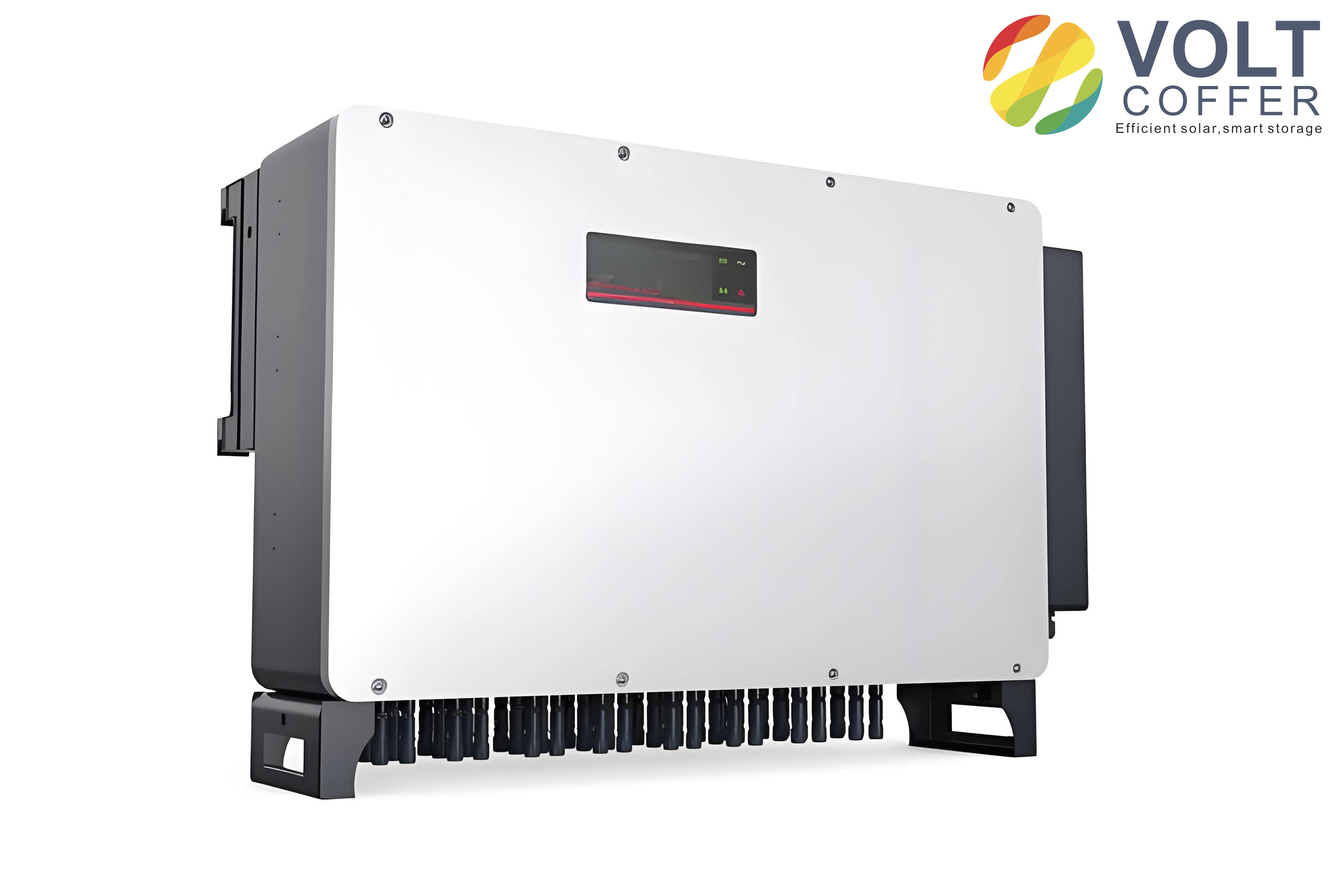
The proposed common-ground double voltage three-level solar inverter topology is illustrated in the figure below. It consists of a PV panel, a voltage-doubling circuit, a three-level circuit, an output filter, and a load. The voltage-doubling circuit includes two switching devices (S1 and S2), a fast-recovery diode (D1), and a flying capacitor (C1). The three-level circuit comprises four switching devices (S3 to S6), another fast-recovery diode (D2), and a second flying capacitor (C2). The output filter is an LC type with inductance \( L_f \) and capacitance \( C_f \), connected to the load \( R_o \). This solar inverter operates in four distinct modes, each contributing to the generation of three-level output waveforms with double the input voltage, thereby improving DC voltage utilization.
The operation of this solar inverter can be divided into four modes, as summarized in Table 1. Each mode corresponds to specific switching states and output SPWM levels, ensuring balanced charging and discharging of the flying capacitors. This balance is crucial for maintaining stable output voltages and minimizing distortion in solar inverters.
| Mode | S1 | S2 | S3 | S4 | S5 | S6 | Output SPWM Level \( u_{spwm} \) |
|---|---|---|---|---|---|---|---|
| M1 | 1 | 0 | 1 | 1 | 0 | 0 | \( 2U_{PV} \) |
| M2 | 0 | 1 | 0 | 1 | 1 | 0 | 0 |
| M3 | 1 | 0 | 1 | 0 | 0 | 1 | 0 |
| M4 | 0 | 1 | 0 | 0 | 1 | 1 | \( -2U_{PV} \) |
In Mode M1, switches S1, S3, and S4 are turned on. The current flows from the PV positive terminal through S1, C1, S3, and S4 to the load, while C2 is charged via D2. The output voltage \( u_{spwm} \) is \( 2U_{PV} \), as the PV voltage and C1 discharge combine. This mode demonstrates how the solar inverter achieves voltage doubling, enhancing the efficiency of power conversion. In Mode M2, switches S2, S4, and S5 are on, resulting in \( u_{spwm} = 0 \). Here, C1 is charged, and C2 is idle, providing a zero state during the positive half-cycle. Mode M3 involves S1, S3, and S6 being on, with C2 charged by the PV and C1, and \( u_{spwm} = 0 \) for the negative half-cycle zero state. Finally, in Mode M4, switches S2, S5, and S6 are on, and C2 discharges to produce \( u_{spwm} = -2U_{PV} \), while C1 is charged. These modes ensure that the flying capacitors in the solar inverter maintain balanced energy states, preventing voltage drift and improving reliability.
The modulation strategy for this solar inverter employs a carrier stacking technique with SPWM. As shown in Figure 5, a sinusoidal reference wave \( u_r \) is compared with two triangular carrier waves \( u_{C1} \) and \( u_{C2} \), as well as a ground signal. When \( u_r \) exceeds a carrier or ground, the output is 1; otherwise, it is 0. This generates preprocessed signals A, B, and C, which are then logically combined to produce the gate signals for switches S1 to S6. The logical expressions are:
$$ S1 = S3 = A + BC $$
$$ S4 = C $$
$$ S2 = S5 = \overline{S1} $$
$$ S6 = \overline{S4} $$
This modulation scheme simplifies control and ensures accurate generation of the three-level output in the solar inverter, making it suitable for real-time implementation. The use of carrier stacking allows for precise regulation of the output voltage and current, which is essential for grid-connected solar inverters.
Selecting the appropriate flying capacitors is critical for the performance of the solar inverter. The negative voltage level is primarily supplied by C2, so its discharge energy must match the load demand. Based on energy conservation, the voltage ripple \( \Delta u_{C2} \) of C2 can be derived. During Mode M4, the energy discharged from C2 equals the energy absorbed by the load:
$$ \frac{1}{2} C_2 \left[ u_{C2}(t_1)^2 – u_{C2}(t_2)^2 \right] = \int_{t_1}^{t_2} u_o i_o \, dt $$
Assuming \( u_o = U_o \sin(\omega t) \) and \( i_o = I_o \sin(\omega t) \), and simplifying, we get:
$$ C_2 = \frac{ U_o I_o \left[ \Delta t – \frac{1}{2\omega} \left( \sin(2\omega t_2) – \sin(2\omega t_1) \right) \right] }{ \Delta u_{C2} \left[ 2u_{C2}(t_1) – \Delta u_{C2} \right] } $$
where \( \Delta t = t_2 – t_1 \). This equation helps determine the capacitance value to limit voltage ripple, ensuring stable operation of the solar inverter. A larger capacitance reduces ripple but increases cost, so a trade-off is necessary based on application requirements.
To validate the design, I conducted simulations using Simulink with parameters listed in Table 2. The proposed solar inverter was compared to a conventional oH5 transformerless solar inverter and a common-ground five-switch solar inverter from literature. The simulations focused on output voltage \( u_o \), output current \( i_o \), SPWM levels \( u_{spwm} \), common-mode voltage \( u_{cm} \), and leakage current \( i_{cm} \). Under a DC input voltage of 100 V, the proposed solar inverter achieved an output voltage of 110 V RMS and current of 0.917 A RMS, whereas the others only reached 55 V RMS and 0.458 A RMS. The SPWM levels ranged from -200 V to 200 V for the proposed design, compared to -100 V to 100 V for the others. Importantly, the common-mode voltage was zero for the common-ground solar inverters, resulting in no leakage current, while the oH5 solar inverter exhibited a leakage current of approximately 1 mA. These results highlight the superiority of the proposed solar inverter in terms of voltage utilization and leakage current elimination.
| Parameter | Value | Parameter | Value |
|---|---|---|---|
| DC Input Voltage | 100 V | Filter Inductance | 5 mH |
| Output Frequency | 50 Hz | Filter Capacitance | 2 μF |
| Output Voltage RMS | 110 V | Flying Capacitor C1 | 220 μF |
| Rated Power | 100 W | Flying Capacitor C2 | 390 μF |
| DC Link Capacitance | 220 μF | Parasitic Capacitance | 100 nF |
| Switching Frequency | 30 kHz | – | – |
Experimental results from a 100 W prototype further confirmed the simulation findings. The prototype used IPP60R125C6 MOSFETs and SF2040CT fast-recovery diodes, with parameters matching Table 2. Under full load, the output voltage and current waveforms for the proposed solar inverter showed a peak SPWM level of 200 V, compared to 100 V for the common-ground five-switch solar inverter. Leakage currents were negligible in both common-ground solar inverters, as expected. The output SPWM waveform exhibited clean three-level transitions, and the flying capacitors maintained balanced voltages, demonstrating the effectiveness of the modulation strategy. These experiments underscore the practical viability of this solar inverter for real-world applications, offering enhanced performance without compromising safety.
In conclusion, the common-ground double voltage three-level single-phase transformerless solar inverter presented here addresses key challenges in PV systems. By integrating a common-ground connection, it completely eliminates leakage currents, ensuring compliance with safety standards. The double-voltage operation and three-level output improve DC voltage utilization, reducing the need for higher input voltages or additional components. The modulation strategy based on carrier stacking is straightforward and efficient, facilitating implementation. Simulation and experimental results validate the design, showing superior performance compared to existing solar inverters. Future work could explore scalability to higher power levels and integration with maximum power point tracking (MPPT) for optimized solar energy harvesting. This solar inverter topology represents a significant advancement in transformerless technology, contributing to more efficient and reliable renewable energy systems.