
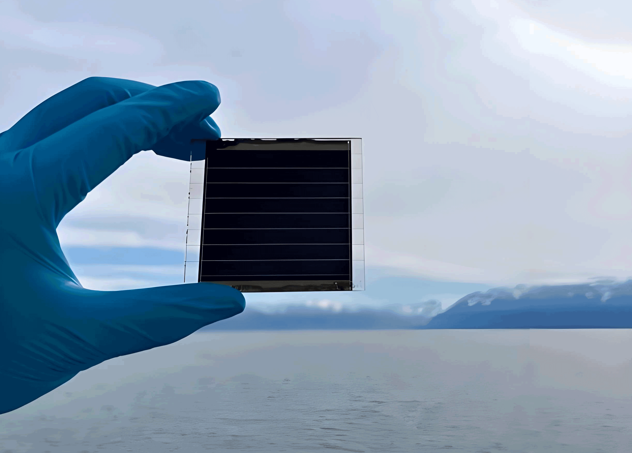
In recent years, perovskite solar cells have emerged as a promising technology for next-generation photovoltaics due to their high power conversion efficiencies, low-cost fabrication, and tunable optoelectronic properties. However, the performance of these devices is often limited by non-radiative recombination losses at the buried interface between the perovskite light-absorbing layer and the electron transport layer (ETL). Specifically, tin dioxide (SnO2) ETLs prepared via chemical bath deposition (CBD) commonly exhibit a high density of oxygen vacancy defects, which act as trapping sites for charge carriers and reduce the overall efficiency and stability of perovskite solar cells. To address this issue, we developed a bimolecular passivation strategy using tin tetrachloride (SnCl4) and ammonium chromate ((NH4)2CrO4) to modify the SnO2/perovskite interface. This approach not only passivates surface defects but also enhances charge extraction, leading to a significant improvement in the performance of perovskite solar cells.
The fabrication of perovskite solar cells involves several critical steps, including the deposition of the ETL, perovskite layer, hole transport layer, and electrodes. For the ETL, we utilized a CBD method to prepare SnO2 films on fluorine-doped tin oxide (FTO) substrates. The SnO2 layer was then treated with a bimolecular solution containing SnCl4 and (NH4)2CrO4 to passivate the buried interface. The perovskite active layer was formed using a cesium-doped formamidinium lead iodide (Cs-FAPbI3) composition, followed by the deposition of a spiro-OMeTAD hole transport layer and gold electrodes. For comparison, we also prepared control devices without passivation and with individual passivation using SnCl4 or (NH4)2CrO4. The key parameters for the device fabrication are summarized in Table 1.
| Component | Material/Process | Conditions |
|---|---|---|
| ETL | SnO2 via CBD | 70°C for 3 h, annealed at 180°C |
| Passivation | SnCl4 and (NH4)2CrO4 | Spin-coating at 3000 rpm, annealed at 180°C |
| Perovskite | Cs-FAPbI3 | Spin-coating and annealing at 160°C |
| HTL | Spiro-OMeTAD | Spin-coating at 3000 rpm |
| Electrode | Gold | Thermal evaporation |
The photovoltaic performance of the perovskite solar cells was evaluated under standard AM 1.5G illumination. The current-density-voltage (J-V) characteristics revealed that the bimolecularly passivated devices achieved a champion power conversion efficiency (PCE) of 23.71%, with an open-circuit voltage (Voc) of 1.14 V, a short-circuit current density (Jsc) of 26.21 mA/cm2, and a fill factor (FF) of 79.35%. In contrast, the control device without passivation exhibited a PCE of 22.14%, while devices with individual SnCl4 or (NH4)2CrO4 passivation showed PCEs of 22.94% and 22.95%, respectively. The enhancement in PCE for the bimolecularly passivated perovskite solar cells is attributed to the synergistic effects of defect passivation and improved charge transport. The external quantum efficiency (EQE) spectra further confirmed the superior performance, with the integrated current densities aligning closely with the Jsc values obtained from J-V measurements. The statistical distribution of photovoltaic parameters across multiple devices is provided in Table 2, demonstrating the reproducibility and reliability of the bimolecular passivation approach.
| Passivation Type | Voc (V) | Jsc (mA/cm2) | FF (%) | PCE (%) |
|---|---|---|---|---|
| Control | 1.12 ± 0.01 | 25.87 ± 0.10 | 75.96 ± 0.50 | 22.00 ± 0.14 |
| SnCl4 only | 1.12 ± 0.01 | 25.79 ± 0.12 | 78.76 ± 0.40 | 22.75 ± 0.19 |
| (NH4)2CrO4 only | 1.12 ± 0.01 | 25.51 ± 0.15 | 78.73 ± 0.45 | 22.49 ± 0.21 |
| Bimolecular | 1.14 ± 0.01 | 26.17 ± 0.08 | 79.22 ± 0.35 | 23.63 ± 0.12 |
To understand the morphological changes induced by the bimolecular passivation, we performed scanning electron microscopy (SEM) analysis. The unpassivated SnO2 film exhibited a rough surface with visible FTO crystal grains, whereas the bimolecularly passivated SnO2 film showed a smoother and more uniform surface due to the formation of small SnO2 nanoparticles from the hydrolysis of SnCl4. This平整的表面结构 facilitated the growth of larger perovskite grains with reduced grain boundaries, as observed in the SEM images of the perovskite layers. The reduction in grain boundaries is critical for minimizing defect densities in perovskite solar cells, as grain boundaries often serve as recombination centers for charge carriers. The improved morphology directly contributes to the enhanced performance of the bimolecularly passivated perovskite solar cells.
X-ray photoelectron spectroscopy (XPS) was employed to investigate the chemical states and defect passivation at the SnO2 surface. The Sn 3d spectra of the unpassivated SnO2 showed peaks at 495.6 eV and 487.2 eV, corresponding to Sn 3d3/2 and Sn 3d5/2, respectively. After bimolecular passivation, these peaks shifted to lower binding energies (495.4 eV and 487.0 eV), indicating the formation of Sn-O-Cr bonds and the creation of a p-n junction between Cr2O3 and SnO2. The O 1s spectra were deconvoluted into two components: lattice oxygen at 531.2 eV and non-lattice oxygen (e.g., O−, O2−, OH−) at 532.1 eV. The ratio of non-lattice oxygen decreased from 49% in the unpassivated SnO2 to 31% in the bimolecularly passivated sample, confirming the effective passivation of oxygen vacancies. This reduction in surface defects is essential for minimizing non-radiative recombination in perovskite solar cells.
The electrical properties of the devices were further analyzed using space-charge-limited current (SCLC) measurements. The trap-filled limit voltage (VTFL) was derived from the I-V characteristics of electron-only devices with the structure FTO/SnO2/perovskite/PCBM/Ag. The VTFL decreased from 0.434 V for the unpassivated device to 0.344 V for the bimolecularly passivated device, indicating a reduction in trap density. The trap density (Nt) can be calculated using the formula:
$$N_t = \frac{2 \epsilon_0 \epsilon_r V_{\text{TFL}}}{e L^2}$$
where $\epsilon_0$ is the vacuum permittivity, $\epsilon_r$ is the relative permittivity of the perovskite, $e$ is the electron charge, and $L$ is the thickness of the perovskite layer. For the unpassivated device, Nt was calculated to be 2.91 × 1015 cm−3, while for the bimolecularly passivated device, it reduced to 2.31 × 1015 cm−3. This decrease in trap density aligns with the observed improvement in Voc and FF, as lower trap densities reduce charge recombination in perovskite solar cells. Additionally, the dark current measurements showed a lower leakage current for the passivated devices, further confirming the suppression of defect-mediated recombination.
Steady-state photoluminescence (PL) spectroscopy was conducted to evaluate the carrier recombination dynamics in the perovskite layers. The PL intensity of the perovskite film deposited on the bimolecularly passivated SnO2 was significantly higher than that on the unpassivated SnO2, with both films exhibiting a peak emission wavelength of 799 nm. The enhanced PL intensity indicates a reduction in non-radiative recombination pathways, which is consistent with the passivation of interface defects. In perovskite solar cells, the formation of a Cr2O3/SnO2 p-n junction not only passivates defects but also facilitates electron extraction, leading to a balance between reduced recombination and efficient charge collection. This dual mechanism explains the overall performance enhancement in the bimolecularly passivated perovskite solar cells.
The mechanism of bimolecular passivation involves multiple synergistic effects. SnCl4 hydrolyzes to form Sn(OH)4, which subsequently decomposes into small SnO2 nanoparticles that fill the voids between the larger SnO2 grains, resulting in a smoother surface. This process is accompanied by the recrystallization of SnO2 under the influence of hydrochloric acid produced during hydrolysis, which reduces surface roughness and suppresses particle aggregation. Concurrently, (NH4)2CrO4 decomposes upon heating to form NH3, H2O, and Cr2O3. The Cr2O3 layer acts as a p-type semiconductor and compensates for the oxygen vacancies on the SnO2 surface. The resulting p-n junction between Cr2O3 and SnO2 enhances electron extraction by allowing tunneling through the thin Cr2O3 layer, while also blocking electron back-transfer to the perovskite layer. This combination of effects reduces non-radiative recombination at the buried interface and improves the charge collection efficiency in perovskite solar cells. Furthermore, the smoother SnO2 surface promotes the growth of larger perovskite grains with fewer defects, contributing to the enhanced stability and performance of the devices.
The stability of the perovskite solar cells was assessed by monitoring the normalized PCE under ambient conditions (25°C and 35% relative humidity) in the dark. The unencapsulated bimolecularly passivated devices retained 85% of their initial PCE after 1,440 hours, whereas the control devices and those with individual passivation retained only 58%, 68%, and 71%, respectively. The improved stability is attributed to the reduced defect density and suppressed ion migration at the buried interface, which are common degradation pathways in perovskite solar cells. The bimolecular passivation strategy thus not only enhances the efficiency but also extends the operational lifetime of perovskite solar cells.
In conclusion, we have demonstrated a bimolecular passivation approach using SnCl4 and (NH4)2CrO4 to address the issue of oxygen vacancy defects at the SnO2/perovskite buried interface. This method synergistically passivates surface defects, forms a p-n junction to enhance charge extraction, and promotes the growth of high-quality perovskite films. As a result, the bimolecularly passivated perovskite solar cells achieve a high PCE of 23.71% with improved stability. This work highlights the importance of interface engineering in advancing the performance and reliability of perovskite solar cells, and the bimolecular strategy offers a versatile pathway for optimizing other optoelectronic devices.