
In many publications currently issued, the remarkable characteristics and technical advantages of new high-power SiC devices in different applications have been emphasized. Usually, due to SiC devices reducing switching losses and increasing switching frequency, the size of external passive devices will be reduced, improving conversion efficiency.
In solar inverter systems, the use of new silicon carbide devices such as SiC-IGBT is usually aimed at improving power density and power efficiency, and reducing the cost of passive devices and heat sinks.
Due to the difficulty of SiC device production technology and the relatively high device prices, it remains a problem to use SiC devices in the cost sensitive photovoltaic inverter market.
In the article, the focus will be on the cost control of grid connected PV inverter systems. Proposing and explaining the selection and redesign of using SiC device solutions will also evaluate the potential advantages of using SiC devices in photovoltaic inverter systems.
1. Technical route of grid connected photovoltaic equipment
1.1 Overview
Grid-connected PV power devices have different topologies and power inversion systems, such as series inverters, integrated AC inverter photovoltaic board systems, central inverters, and multi-level series inverters.
Due to the different voltage and power levels of photovoltaic equipment, it is necessary to choose different topologies and optimal solutions to transmit the electricity collected by PV panels to the grid, while achieving maximum efficiency tracking.
Several technical routes will be discussed here. In order to improve efficiency while meeting technical specifications and standards, some photovoltaic systems do not have grid connected transformers and are directly integrated into the power grid. The most common topology now is a transformer free multi-level series connected grid inverter.
1.2 Introduction to Transformer Free Multi branch Series PV Inverter System
Figure 1 below is a typical schematic diagram of a multi branch series inverter system. The PV system consists of branch A and branch B, which have different power input conditions, allowing them to operate independently and efficiently. At sunrise or sunset, the PV power equipment is not in the optimal power generation position, and the surrounding roof will cover the battery cells to reduce power. Such cells can be connected to the B input, while the PV battery cells that provide the most power are connected to the A input.
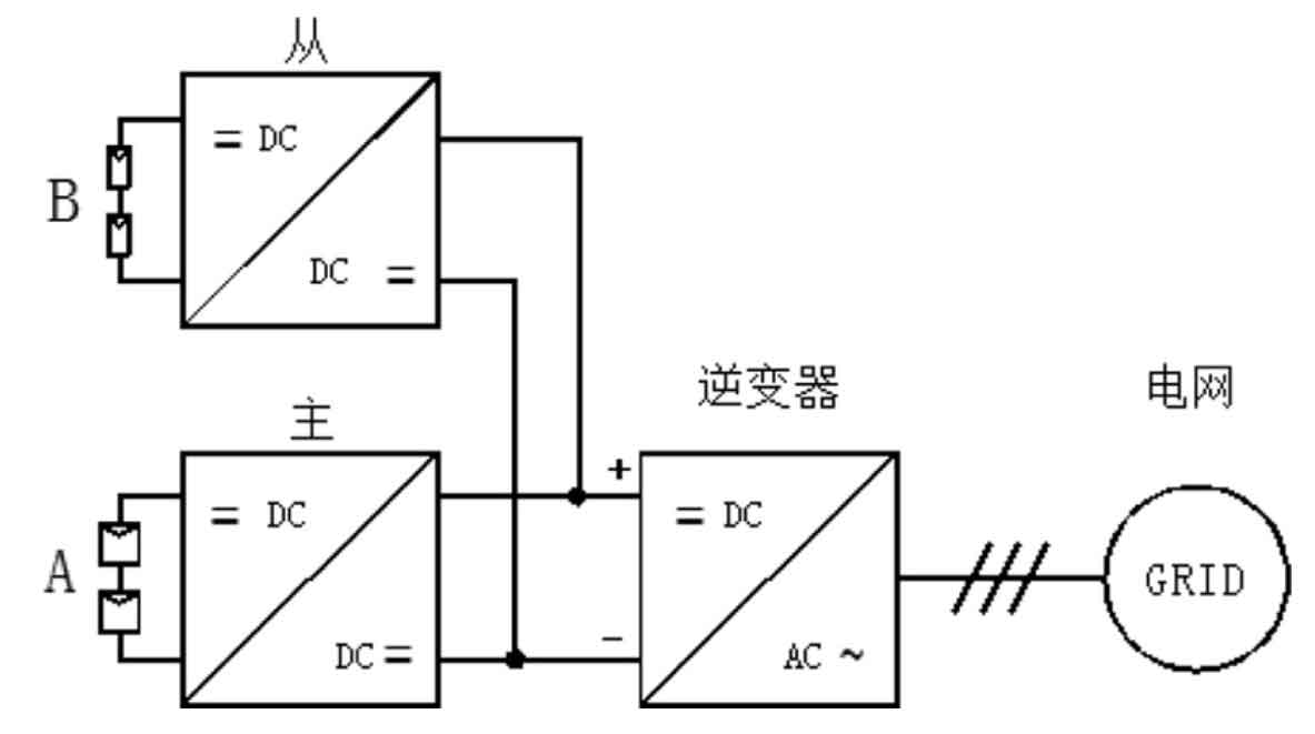
Two DC DC switches operate independently of each other, forming a DC link. In order to achieve optimal efficiency, the DC-DC converter operates in maximum power tracking mode, and the DC/AC converter generates three-phase sinusoidal AC power with the same grid frequency and is integrated into the grid.
The typical multi branch PV solar inverter circuit diagram for three-phase AC400V power grid system is shown in Figure 2.
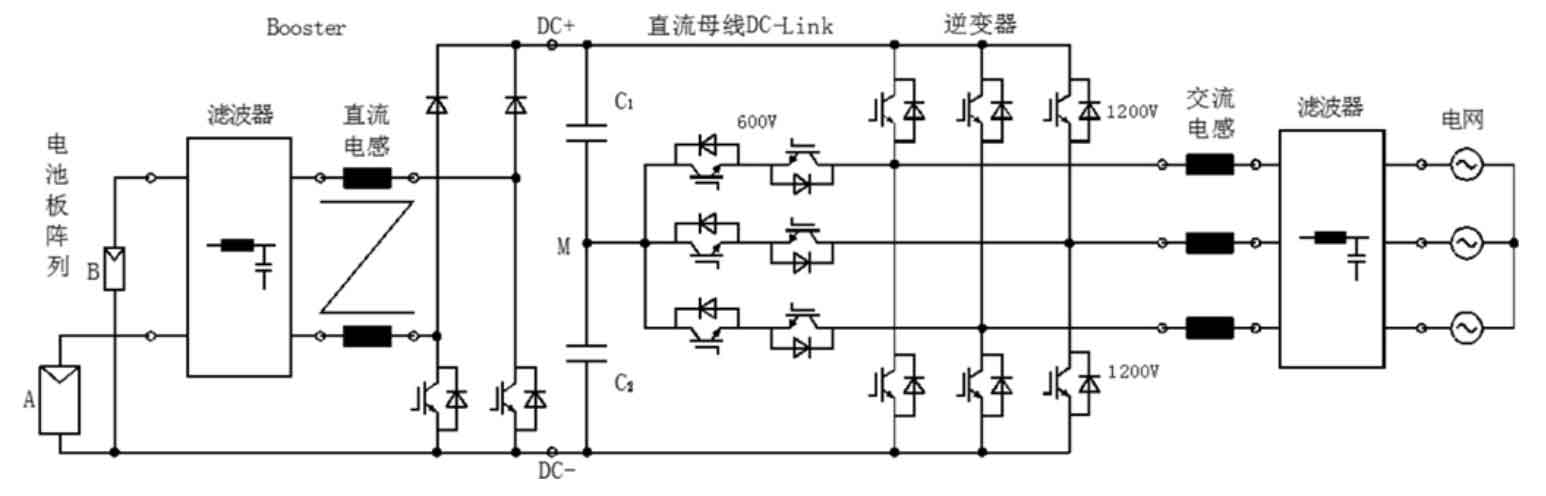
The boost converter will adapt to the input voltage of the PV battery pack and be connected to the DC link through a DC inductor Ldc, with a DC rated voltage of DC600V and a maximum of DC800V. When the IGBT switch frequency is selected as 16kHz, the DC DC inductance value is taken as Ldc=9mH. In order to reduce EMI radiation between the switch device and the electrical floating or grounding of the battery board in boost switching, a low-pass filter needs to be added in the middle.
The midpoint clamped three-level full bridge inverter uses a 1200VSi switching device to transform the DC DC voltage. Through PWM modulation, the DC power is transformed into three-phase rectangular AC power. Through a filtering circuit composed of AC inductance LAC, the voltage waveform is sinusoidal and integrated into the power grid.
In the experiment, the rated output power of the inverter PN=20kW, and when the three-phase grid voltage Uac=400V, the effective output current Iout. N.rms=30A. Adopting a Si three-level topology, using the best Si IGBT and parallel diodes, the switching frequency can reach fsw=15kHz.
According to the principle that the maximum ripple current is equal to 10% of the rated current, the inductance value of AC inductor LAC can be taken as 2 5mH.
Finally, in order to further attenuate and limit residual harmonics, a low-pass filter is installed between the AC inductor and the output end, with a cutoff frequency of F-3dB=150kHz. This is a regulation for civil and industrial EMI in EN61000-6-1 and EN61000-6-2 standards.
| Project | Name | Parameter |
| Radiator temperature | Ths [℃] | 100 |
| Output frequency | Fout [Hz] | 500 |
| Rated output current | Iout, rms, N [A] | 25 |
| DC voltage | UDC [ V ] | 650 |
| Switching frequency | Fsw [kHz] | 16 |
| Power factor | Cos φ | 1 |
| Rated output power | Pout, N [kW] | 17 |
This system is a multi branch transformerless grid connected PV inverter system that includes a Si IGBT boost converter and a three-level inverter. Currently, many PV inverter companies adopt this solution. In the fierce market competition, they expect the cost of the inverter to be significantly reduced. In the future, we will focus on discussing the solution of using SiC devices.
2. Optimization approach for PV inverter system
The main improvement of the existing PV inverter system is to reduce the overall cost. Although the efficiency of PV inverter systems has reached 98% and is no longer the focus of research and development, efficiency has become a prerequisite for the success of a system.
The current trend is that increasing the switching frequency is a very effective means to reduce system costs. Here, SiC devices provide an ideal solution that not only has extremely low conduction loss, but also maintains good electrical performance at ultra-high frequencies. For such a system, if the frequency listed in Table 1 (16kHz) is tripled, it is necessary to explore how much space is available to reduce the inductance and volume of AC and DC inductors, as well as the volume of heat sinks, by using SiC devices.
2.1 Silicon carbide (SiC) IGBT module.
At present, SiC is a non eye-catching material, and the diodes and switch devices manufactured using it are superior to Si devices in almost every aspect. Especially the switch loss is significantly reduced.
2.2 Technical Route of SiC Semiconductor
Booster part:
The Booster system consists of Si IGBT. When the maximum temperature Ths of the heat sink is 100 ℃ and the frequency fsw is 16kHz, the chip junction temperature Tvj.op value of the device can be evaluated using Infineon professional evaluation tools.
Using SiC devices instead of Si-IGBTs, several Si-FWDs in Booster will be replaced with SiC diodes. At this point, the frequency of SiC devices can reach 45kHz, which will ultimately reduce the boost inductance from 9mH (LDC) to LDC=3mH.
Inverter part:
The topology structure of the inverter system is shown in Figure 2. The main switch device adopts 1200V Si IGBT, with each anti parallel 1200V Si diode. The inverter neutral terminal is achieved using 600V Si diode and IGBT. The operating status of the system is shown in Table 1. Figure 3 lists three possible ways to achieve PV inverters, with only single-phase depicted in the figure.
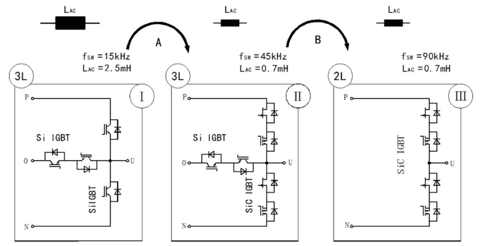
In step A, in order to increase the switching frequency, the Si-IGBT of module (I) is replaced with SiC devices. After replacement, the inductance value can be reduced to 1/3 of the original value while maintaining the same current level at three times the frequency (45kHz), and the AC inductance value can be reduced from 2 Reduce 1mH to 0 At 7mH, due to the increase in frequency, ultra microcrystalline materials can be selected, resulting in a significant reduction in inductance volume and value.
When the inverter is running, usually a single transistor SiC-IGBT needs to be connected in series with a low-voltage P-channel MOSFET to achieve normally closed characteristics. To ensure safe operation in the event of gate power outage or short circuit, a gate driver chip is usually needed to control the IGBT/MOS-FET cascade device.
As shown in Figure 3, through step B, in order to promote the reduction of system cost, the IGBT neutral point branch was simplified and converted into a two-level inverter topology (2L) to ensure the same current ripple (LAC=0 The frequency of 7mH needs to be increased to 90kHz. The number of gate drive units and the complexity of gate control will be reduced.
| Plan | System part | Topology | Fs [kHz] | AC/DC inductance [mH] | Tvj.op main switch [℃] |
| a) | Booster | Booster | 15 | 9 | 150 |
| b) | Booster | Booster | 45 | 3 | 125 |
| I | Inverter | Three level NPC2 | 15 | 2.1 | 150 |
| II | Inverter | Three level NPC2 | 45 | 0.7 | 120 |
| III | Inverter | Two level | 90 | 0.7 | 130 |
Due to the superior performance of SiC, it is possible to optimize the entire PV inverter system, which can reduce the total loss of the equipment and improve work efficiency.
3. System cost-benefit analysis
The cost model mainly consists of three parts: power module, magnetic components, and heat sink. These parts are organically combined through technical methods in PV inverter systems, and they are the main components of the cost of PV inverter systems.
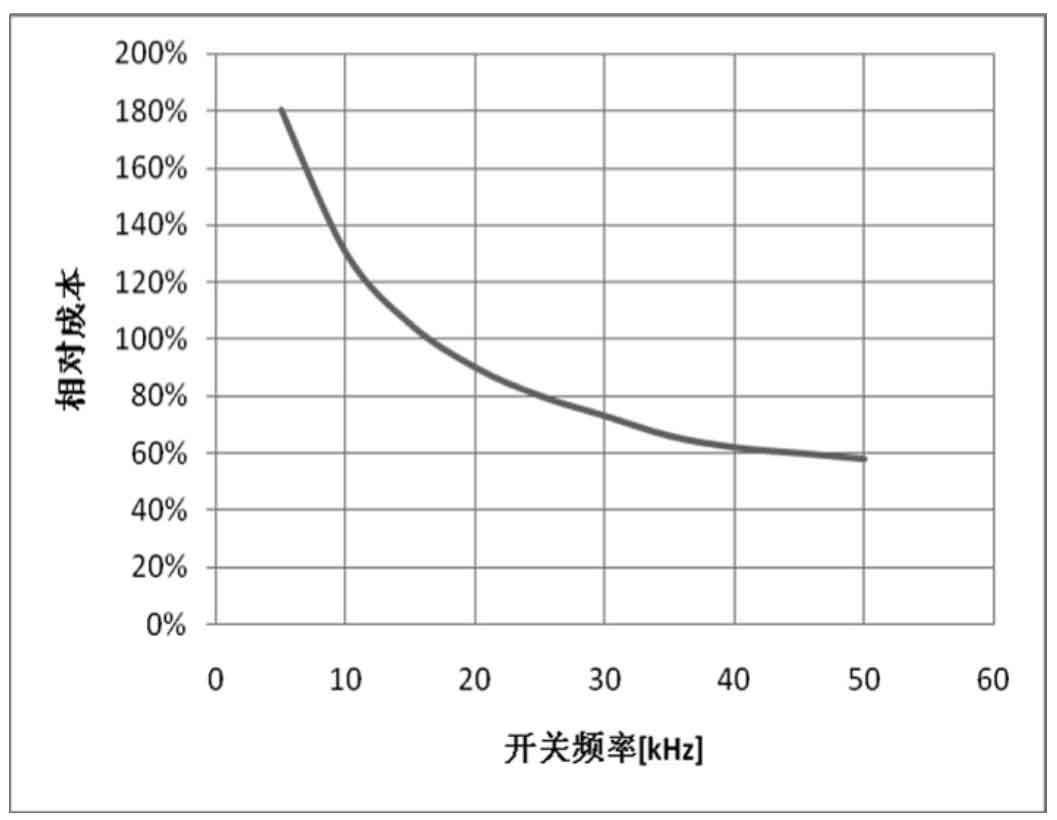
According to market analysis, the cost of magnetic components follows the square root principle. When the switching frequency is increased from 16kHz to 30kHz, the cost decreases to 70% of the initial investment. When it is increased to 45kHz, the cost decreases to 60% of the initial investment, as shown in Figure 4.
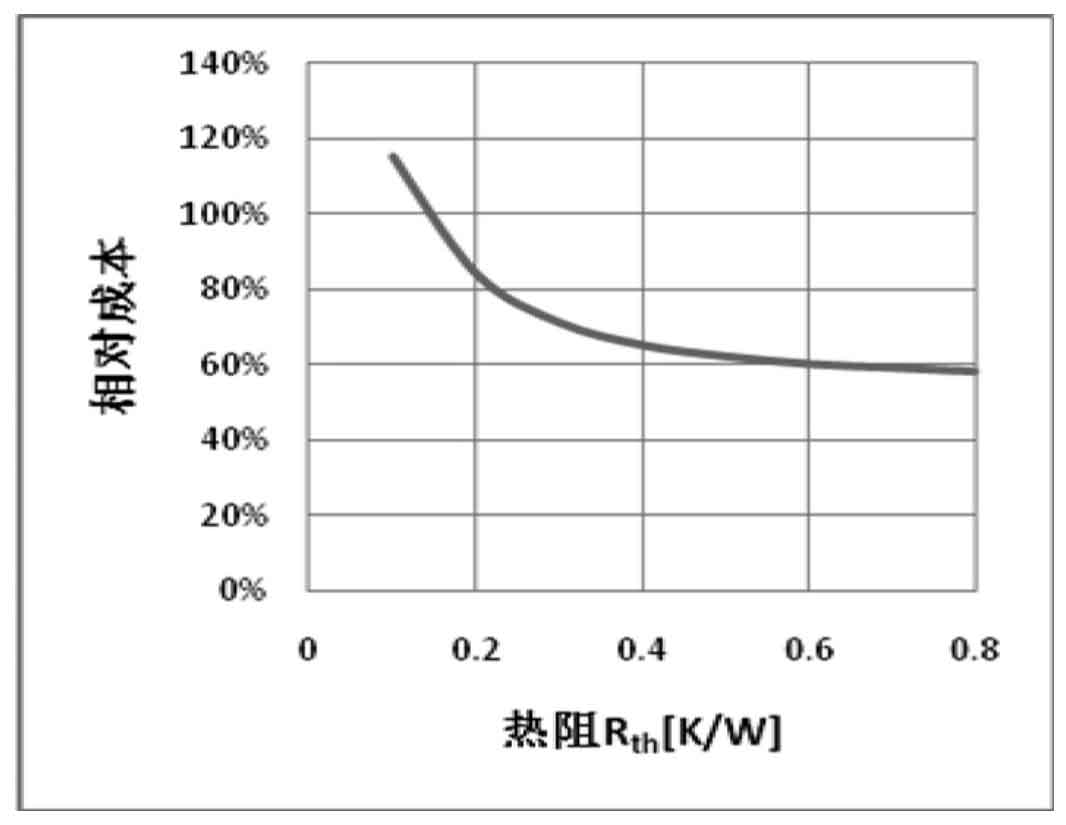
Figure 5 shows the function curve between the thermal resistance and cost of the radiator. When evaluating the radiator, all raw materials and full size are used as input parameters to establish models of different sizes of radiators.
| Plan | Booster | Inverter | Maximum system power consumption | Cost |
| 1) | Si+SiC | Three level IGBT | 732W | 100% |
| 2) | SiC+SiC | Two level SiC | 514W | 82% |
| 3) | SiC+SiC | Three level SiC | 381W | 80% |
In the previous chapters, different technical solutions were listed to establish the relationship between the switching frequency, chip junction temperature Tvj op, and power loss for the boost and inverter. At the same time, the cost dependency relationship was also discussed in the previous chapters, which includes the three main components of PV inverters, namely magnetic components, heat sinks, and power modules. When designing, assuming that the output power is constant, the DC-link and other current carrying devices remain unchanged, the typical contribution of these three components to the cost of the inverter is approximately 50%.
Taking the three-level Si IGBT scheme as a reference, it can be seen that the system cost has been reduced by 20% after using SiC devices. Of course, accurate savings depend on the final design parameters of the actual system. Among all the selected options, although the options are different, the savings are similar. More importantly, the increase in switching frequency and the reduction in heat sink are proportional in modeling. In all cases, due to the high cost of SiC converters, the cost of power modules is also increasing. However, the excess is compensated for by superior technical performance. Extremely low switching losses can increase the switching frequency, effectively reducing the cost of magnetic components, while reducing the size of the heat sink and reducing costs.
4. Conclusion
In this article, several technical solutions that can reduce the cost of multi branch PV inverter systems are introduced. In the first part, different schemes using SiC switching devices were discussed, and the effects on main operating parameters such as Tvj-op and fs were listed. Cost models for magnetic components, heat sinks, and power modules were derived, all of which were affected by SiC. At the same time, they contributed significantly to the cost of PV inverter systems. For devices, using cost models to link design and operation, SiC solutions can save costs by 20%. It can be comparable to the three-level Si scheme [5]. Among these two schemes, although SiC has a higher cost, its performance is excellent. Under the same efficiency, better switching loss performance can achieve higher switching frequency and reduce heat sink size.