
In recent years, perovskite solar cells have emerged as a transformative technology in photovoltaics, with certified power conversion efficiencies soaring to over 26% within a decade. This rapid progress is largely attributed to the exceptional optoelectronic properties of organic-inorganic hybrid perovskite materials, including high absorption coefficients, superior charge carrier mobility, and long diffusion lengths. However, the majority of high-efficiency devices are based on polycrystalline thin films, which suffer from intrinsic limitations such as grain boundaries that act as recombination centers and pathways for ion migration, ultimately compromising both efficiency and stability. In contrast, single-crystal perovskites, free from grain boundaries, exhibit significantly lower defect densities, enhanced optoelectronic characteristics, and improved environmental stability. These advantages position perovskite single-crystal solar cells as promising candidates for next-generation photovoltaic applications, offering the potential to overcome the bottlenecks associated with polycrystalline counterparts.
The development of perovskite single-crystal solar cells hinges on the fabrication of high-quality, large-area single-crystal thin films with controlled thicknesses. Traditional bulk single crystals, while possessing excellent material properties, are too thick (often millimeters) for efficient charge carrier extraction in solar cells, as their thickness far exceeds the typical carrier diffusion lengths. Thus, methods to produce micrometer-thin single-crystal perovskites have become a focal point of research. Various techniques have been explored, including vapor-phase epitaxy, surface tension-assisted growth, top-down approaches, and space-confined growth. Among these, space-confined growth has proven particularly effective, enabling the direct synthesis of single-crystal thin films on substrates with predefined thicknesses, which is crucial for integrating them into functional devices like perovskite solar cells.
Vapor-phase epitaxy involves the growth of single-crystal thin films on lattice-matched substrates under controlled temperature and pressure conditions. For instance, studies have demonstrated the epitaxial growth of CsPbBr3 single-crystal thin films on substrates such as NaCl or SrTiO3, resulting in crystals with low defect densities on the order of 1012 cm−3. The process relies on precise lattice matching between the perovskite and the substrate, which can be described by the lattice mismatch parameter:
$$ \delta = \frac{|a_s – a_p|}{a_p} \times 100\% $$
where \( a_s \) and \( a_p \) are the lattice constants of the substrate and perovskite, respectively. A low δ value is essential for high-quality epitaxial growth. However, the high temperatures and stringent lattice requirements limit the widespread application of this method for perovskite solar cells.
Surface tension-assisted growth leverages the surface tension of solutions to control nucleation and growth. In this approach, perovskite precursors are dissolved in high-concentration solutions, and crystals nucleate and grow at the solution-air interface, resulting in thin films with thicknesses ranging from 5 to 40 μm. The process can be modeled using the Young-Laplace equation, which relates the pressure difference across the interface to surface tension:
$$ \Delta P = \gamma \left( \frac{1}{R_1} + \frac{1}{R_2} \right) $$
where \( \gamma \) is the surface tension, and \( R_1 \) and \( R_2 \) are the principal radii of curvature. Modifications, such as using aqueous solvents, have improved growth rates and crystal quality, but controlling lateral dimensions remains challenging.
Top-down methods involve slicing or etching bulk single crystals to achieve thin layers. For example, diamond wire cutting has been used to produce inch-sized FAPbI3 single-crystal wafers with thicknesses around 100 μm. Subsequent chemical etching can further reduce the thickness to below 20 μm. The etching rate can be expressed as:
$$ \frac{dh}{dt} = k C^n $$
where \( h \) is thickness, \( t \) is time, \( k \) is the rate constant, \( C \) is etchant concentration, and \( n \) is the reaction order. Despite progress, the brittleness of perovskite crystals poses significant challenges in achieving uniform, large-area thin films.
Space-confined growth has emerged as the most versatile technique for producing single-crystal thin films for perovskite solar cells. This method involves confining the perovskite precursor solution between two substrates separated by spacers, controlling the film thickness precisely. The growth kinetics can be described by diffusion-limited models, where the crystal thickness \( d \) is proportional to the square root of time:
$$ d = \sqrt{D t} $$
where \( D \) is the diffusion coefficient. A key advancement was the use of hydrophobic substrates (e.g., ITO/PTAA) to enhance ion migration rates, enabling the growth of millimeter-sized single-crystal thin films with thicknesses of 10–20 μm. This approach allows direct integration into device architectures, simplifying fabrication and improving interface quality for perovskite solar cells.
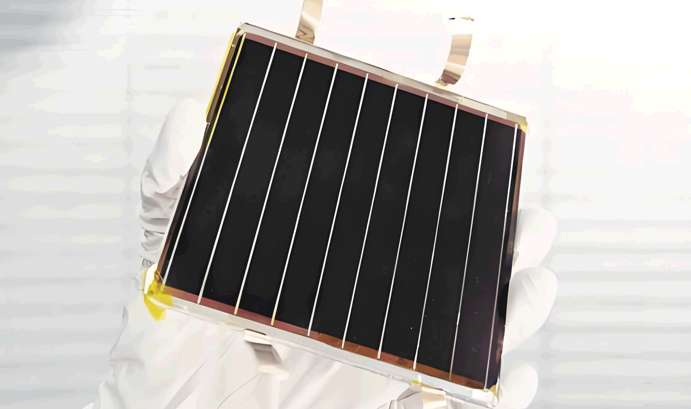
The evolution of high-performance perovskite single-crystal solar cells began with MAPbI3-based devices. Initial n-i-p structures on FTO/TiO2 substrates yielded efficiencies below 9%, limited by thick crystals (50–200 μm) that impeded charge extraction. A breakthrough came with the adoption of p-i-n structures on hydrophobic ITO/PTAA, where surface passivation with MAI reduced defect densities, boosting efficiencies to 17.8%. Further optimizations, such as solvent engineering to lower growth temperatures and the incorporation of mixed hole transport layers (e.g., PTAA:P3HT), enhanced crystal quality and interface properties, pushing efficiencies above 22%. Defect passivation strategies, including the use of multifunctional molecules like MDMS, further improved stability and performance, with reported efficiencies reaching 22.2%.
To broaden the absorption spectrum and improve thermal stability, researchers explored mixed-cation compositions. FA0.6MA0.4PbI3 single-crystal solar cells demonstrated a redshift in absorption edge by approximately 30 nm compared to MAPbI3, leading to higher short-circuit current densities and efficiencies up to 22.8%. Replacing PTAA with hydrophilic self-assembled monolayers (e.g., MeO-2PACz) improved interface adhesion and charge transport, achieving 23.1% efficiency. The incorporation of cesium ions, as in Cs0.05FA0.95PbI3, extended absorption further and enhanced thermal stability, resulting in a record efficiency of 24.3% for perovskite single-crystal solar cells. Surface engineering techniques, such as polishing and hydrophobic modification with CTAC, have also been employed to reduce surface defects and improve moisture resistance, contributing to efficiencies exceeding 23%.
The performance parameters of key perovskite single-crystal solar cells are summarized in Table 1, highlighting the progressive improvements in short-circuit current density (\( J_{sc} \)), open-circuit voltage (\( V_{oc} \)), fill factor (FF), and power conversion efficiency (PCE).
| Device Structure | \( J_{sc} \) (mA/cm²) | \( V_{oc} \) (V) | FF (%) | PCE (%) | Year |
|---|---|---|---|---|---|
| FTO/TiO2/MAPbI3/Spiro-OMeTAD/Au | 22.3 | 0.67 | 59.0 | 8.78 | 2017 |
| ITO/PTAA/MAPbI3/PC61BM/C60/BCP/Cu | 21.0 | 1.08 | 78.6 | 17.8 | 2017 |
| ITO/PTAA/MAPbI3/C60/BCP/Cu | 23.5 | 1.08 | 83.5 | 21.1 | 2019 |
| ITO/PTAA/MAPbI3/C60/BCP/Cu | 23.7 | 1.14 | 81.0 | 21.9 | 2020 |
| ITO/PTAA:P3HT/MAPbI3/C60/BCP/Cu | 23.9 | 1.13 | 81.8 | 22.1 | 2021 |
| ITO/PTAA/MAPbI3/MDMS/C60/BCP/Cu | 24.1 | 1.13 | 81.5 | 22.2 | 2023 |
| ITO/PTAA/FA0.6MA0.4PbI3/C60/BCP/Cu | 26.2 | 1.10 | 79.0 | 22.8 | 2021 |
| ITO/MeO-2PACz/FA0.6MA0.4PbI3/C60/BCP/Cu | 27.5 | 1.07 | 77.0 | 23.1 | 2023 |
| ITO/MeO-2PACz/Cs0.05FA0.95PbI3/C60/BCP/Cu | 28.1 | 1.09 | 79.3 | 24.3 | 2023 |
| ITO/PTAA/Cs0.05FA0.95PbI3/C60/BCP/Cu | 26.0 | 1.09 | 81.6 | 23.1 | 2024 |
| ITO/PTAA/FA0.2MA0.8PbI3/C60/BCP/Cu | 25.2 | 1.10 | 84.4 | 23.4 | 2024 |
| ITO/PTAA/Cs0.05FA0.95PbI3/MDAPb2I6/C60/BCP/Cu | 26.2 | 1.08 | 84.1 | 23.8 | 2024 |
Despite these advancements, several challenges must be addressed to further enhance the performance of perovskite single-crystal solar cells. Thickness control is critical; current devices use crystals between 10–20 μm, which are substantially thicker than polycrystalline films (500–800 nm). While thicker crystals improve light absorption, they also increase the probability of charge carrier recombination. The optimal thickness \( d_{opt} \) for maximizing efficiency can be estimated by balancing absorption and recombination:
$$ d_{opt} = \frac{1}{\alpha} \ln \left( \frac{1}{R} \right) $$
where \( \alpha \) is the absorption coefficient and \( R \) is the reflectance. Reducing thickness below 10 μm without compromising crystal quality remains a significant hurdle, necessitating innovations in growth techniques.
Defect passivation is another key area. Although single crystals have lower bulk defect densities compared to polycrystalline films, surfaces and interfaces still host traps that promote non-radiative recombination. Strategies from polycrystalline perovskite solar cells, such as additive engineering (e.g., Lewis acids/bases) and interface modification with organic molecules or low-dimensional perovskites, can be adapted. The defect density \( N_t \) can be related to the open-circuit voltage loss \( \Delta V_{oc} \) by:
$$ \Delta V_{oc} = \frac{kT}{q} \ln \left( \frac{J_{00}}{J_{0}} \right) $$
where \( k \) is Boltzmann’s constant, \( T \) is temperature, \( q \) is electron charge, \( J_{00} \) is the saturation current density in the absence of defects, and \( J_{0} \) is the actual saturation current density. Effective passivation can reduce \( N_t \) and minimize \( \Delta V_{oc} \), thereby improving efficiency.
Interface contact between the single-crystal thin film and the substrate is crucial for efficient charge transport. Hydrophobic substrates like PTAA facilitate ion migration during growth but often lead to poor adhesion, causing delamination. Optimizing growth conditions, solvent selection, and using alternative hole transport materials (e.g., SAMs) can enhance interface quality. The contact resistance \( R_c \) can be modeled as:
$$ R_c = \frac{1}{q A \mu n} $$
where \( A \) is area, \( \mu \) is mobility, and \( n \) is carrier density. Minimizing \( R_c \) is essential for high fill factors in perovskite solar cells.
Large-area fabrication is imperative for the commercialization of perovskite single-crystal solar cells. Current methods primarily yield small-area crystals (less than 1 cm²), limiting scalability. Techniques compatible with roll-to-roll processing or other industrial methods need development. The efficiency scaling with area \( A \) often follows a power-law relation:
$$ \text{PCE}(A) = \text{PCE}_0 \left( \frac{A_0}{A} \right)^\beta $$
where \( \text{PCE}_0 \) is the efficiency at reference area \( A_0 \), and \( \beta \) is a scaling exponent typically between 0 and 1. Achieving low \( \beta \) values is key to maintaining high performance over large areas.
Standardization and certification are also lacking for perovskite single-crystal solar cells. Unlike polycrystalline devices, which undergo third-party verification, most reported efficiencies for single-crystal cells are from lab measurements. Establishing rigorous testing protocols for stability (e.g., under damp heat, light soaking, and mechanical stress) and efficiency will be vital for benchmarking and commercial adoption.
In conclusion, perovskite single-crystal solar cells represent a promising avenue for achieving high efficiency and stability in photovoltaics. With record efficiencies approaching 25%, they are closing the gap with polycrystalline counterparts. Future progress hinges on overcoming challenges in thickness control, defect management, interface engineering, and scalability. As research efforts intensify, we anticipate that perovskite single-crystal solar cells will not only surpass polycrystalline devices in performance but also pave the way for durable, low-cost solar energy solutions. The continued innovation in growth techniques and material designs will be instrumental in realizing the full potential of perovskite solar cells.