
In recent years, the global energy crisis and environmental pollution have intensified the focus on renewable energy sources, with solar energy standing out as a clean and sustainable option. Perovskite solar cells have emerged as a research hotspot due to their exceptional photovoltaic conversion efficiency and low-cost solution processing techniques. The power conversion efficiency (PCE) of perovskite solar cells has surged from an initial 3.8% to over 26%, highlighting their superior optoelectronic properties and application potential. These advancements are largely attributed to the direct bandgap, high absorption coefficients, and long carrier diffusion lengths of perovskite materials, which facilitate enhanced carrier generation and reduced recombination rates. However, the instability of organic-inorganic hybrid perovskite materials, such as methylammonium lead iodide (MAPbI3), under environmental stressors like moisture, light, and heat, has hindered their commercialization. To address this, inorganic cations like cesium (Cs+) have been employed to replace organic cations, leading to the development of all-inorganic halide perovskites like CsPbBr3. This material exhibits remarkable thermal stability, withstanding temperatures up to 300°C, and offers improved resistance to humidity compared to hybrid counterparts. In this article, I will explore the preparation methods of CsPbBr3 and its applications in perovskite solar cells, emphasizing how these techniques enhance device performance and stability.
CsPbBr3 is a典型的无机钙钛矿材料 with a chemical formula of ABX3, where A is cesium (Cs+), B is lead (Pb2+), and X is bromine (Br-). At room temperature, it crystallizes in an orthorhombic structure, transitioning to tetragonal at 88°C and cubic at 130°C. Its electronic properties include a high electron mobility of approximately 1000 cm²/(V·s), which promotes efficient charge carrier transport in perovskite solar cells. Optically, CsPbBr3 has a direct bandgap of around 2.3 eV, positioning it between CsPbI3 (~1.7 eV) and CsPbCl3 (>3.0 eV), thus balancing light absorption and photovoltaic performance. The material’s high defect tolerance ensures that internal defects only cause shallow energy level transitions, preserving its electronic characteristics. These attributes make CsPbBr3 an ideal candidate for stable and efficient perovskite solar cells, particularly in harsh environmental conditions.
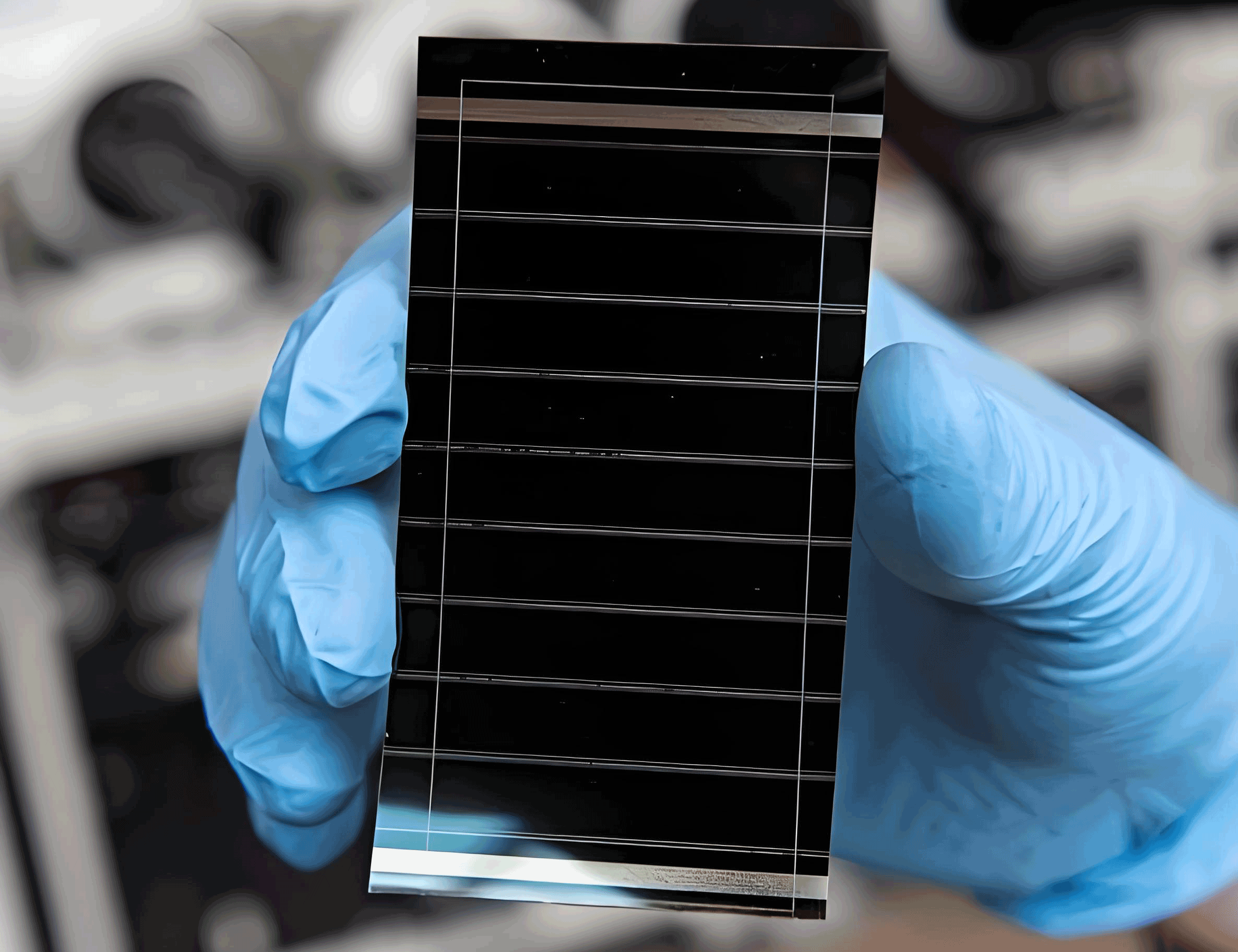
The preparation of CsPbBr3 films is critical for optimizing the performance of perovskite solar cells. Various methods have been developed to control crystallization, reduce defects, and improve interface properties. In the following sections, I will discuss key techniques, including multi-step spin-coating, interface engineering, additive engineering, pulsed laser deposition (PLD), and vapor deposition. Each method offers unique advantages in enhancing the quality of CsPbBr3 films and, consequently, the efficiency and stability of perovskite solar cells.
Multi-step Spin-coating Method
Multi-step spin-coating is a widely used solution-based technique that allows precise control over film formation through sequential coating and annealing steps. By adjusting parameters such as spin speed, annealing temperature, and precursor concentration, researchers can achieve high-quality CsPbBr3 films with reduced defect densities. For instance, in a study involving binary solvents like water and ethanol, optimizing the volume ratio to 60% ethanol resulted in a defect-free, smooth CsPbBr3 film, leading to a perovskite solar cell with a PCE of 7.02%. This approach minimizes heterogeneous and homogeneous nucleation, promoting uniform grain growth and enhancing carrier extraction. Another improvement involved introducing low-concentration CsBr and PbBr2 precursors, which facilitated the formation of a high-quality PbBr2 layer and reduced interface defects. The derived CsPbBr3 film, incorporating phases like CsPb2Br5, exhibited larger grain sizes and fewer grain boundaries, boosting the PCE from 5.43% to 9.36%. Furthermore, by employing solvents like DMF, DMSO, and chlorobenzene and optimizing annealing temperatures (e.g., 100°C), a PCE of 10.02% was achieved, with the device retaining its initial efficiency after 350 days at room temperature and showing only a 10% drop at 120°C. The multi-step spin-coating method thus enables the production of CsPbBr3 films with excellent crystallinity and stability for perovskite solar cells.
To summarize the impact of multi-step spin-coating on CsPbBr3-based perovskite solar cells, I have compiled key performance metrics in Table 1. This table highlights how variations in parameters like solvent composition and annealing conditions influence device outcomes.
| Parameter | Value Range | PCE (%) | Stability |
|---|---|---|---|
| Solvent Ratio (Water:Ethanol) | 60% Ethanol | 7.02 | High |
| Precursor Concentration | Low CsBr/PbBr2 | 9.36 | Enhanced |
| Annealing Temperature | 100°C | 10.02 | >90% after 350 days |
The crystallization process in multi-step spin-coating can be described by the following equation, which relates the grain size (D) to the annealing temperature (T) and precursor concentration (C):
$$ D = k \cdot \exp\left(-\frac{E_a}{RT}\right) \cdot C^{1/2} $$
where \( k \) is a constant, \( E_a \) is the activation energy, \( R \) is the gas constant, and \( T \) is the temperature in Kelvin. This formula underscores how higher annealing temperatures and optimized concentrations lead to larger grains, improving charge transport in perovskite solar cells.
Interface Engineering
Interface engineering focuses on modifying the interfaces between the CsPbBr3 layer and adjacent electron or hole transport layers to enhance charge extraction and minimize non-radiative recombination. For example, the incorporation of natural dyes like curcumin and carotene into CsPbBr3 films has been shown to improve crystallization and passivate defects. Carotene, in particular, reduces vacancies and accelerates carrier generation, increasing the open-circuit voltage (V_oc) of perovskite solar cells. Devices modified with these dyes maintained stability for 90 days in air without encapsulation. Another strategy involves using ammonium chloride (NH4Cl) to修饰 the TiO2/CsPbBr3 interface. Chloride ions passivate surface defects on TiO2, while ammonium ions bond with uncoordinated ions in the perovskite, reducing recombination losses. When combined with zinc phthalocyanine (ZnPc) as a hole transport layer, this approach boosted the PCE from 6.59% to 10.12%. Additionally, the use of carbon quantum dots (CQDs) and red phosphorus quantum dots (RPQDs) at interfaces created intermediate energy levels, facilitating faster charge extraction. This resulted in a PCE of 8.20% and exceptional environmental stability, with only a 3% efficiency drop after 1000 hours at 80% relative humidity. Interface engineering thus plays a pivotal role in optimizing the performance and durability of CsPbBr3-based perovskite solar cells.
Table 2 provides a comparative overview of interface engineering techniques and their effects on CsPbBr3 perovskite solar cells, emphasizing the improvements in PCE and stability.
| Technique | Modification | PCE (%) | Stability Enhancement |
|---|---|---|---|
| Natural Dyes | Curcumin/Carotene | ~7.23 | 90 days in air |
| NH4Cl + ZnPc | TiO2/CsPbBr3 interface | 10.12 | High |
| Quantum Dots | CQDs/RPQDs | 8.20 | 1000 hours at 80% RH |
The charge extraction efficiency at interfaces can be modeled using the following equation for the current density (J) in a perovskite solar cell:
$$ J = J_0 \left( \exp\left(\frac{qV}{nkT}\right) – 1 \right) – J_{sc} $$
where \( J_0 \) is the reverse saturation current, \( q \) is the electron charge, \( V \) is the voltage, \( n \) is the ideality factor, \( k \) is Boltzmann’s constant, \( T \) is temperature, and \( J_{sc} \) is the short-circuit current density. Interface engineering reduces \( J_0 \) by minimizing recombination, thereby increasing \( J_{sc} \) and overall PCE.
Additive Engineering
Additive engineering involves introducing specific materials, such as quantum dots or salts, into the CsPbBr3 precursor solution to regulate crystallization and passivate defects. For instance, the addition of CsPbBr3 or CsPbI3 quantum dots as an intermediate layer between the perovskite and hole transport layer has been demonstrated to optimize energy level alignment and facilitate hole transport. This modification increased the PCE from 5.15% to 7.23% by reducing non-radiative recombination paths. Similarly, incorporating ammonium thiocyanate (NH4SCN) into the precursor solution at a molar ratio of 1.5% significantly improved film quality, leading to enhancements in V_oc, short-circuit current density (J_sc), fill factor (FF), and PCE. Additive engineering not only refines the morphological properties of CsPbBr3 films but also enhances the operational stability of perovskite solar cells, making it a valuable approach for large-scale production.
To illustrate the role of additives, Table 3 summarizes key additives and their impacts on CsPbBr3 perovskite solar cells.
| Additive | Function | PCE Improvement (%) | Key Benefits |
|---|---|---|---|
| CsPbBr3 QDs | Defect passivation | 5.15 to 7.23 | Enhanced hole transport |
| NH4SCN (1.5%) | Film quality optimization | Significant | Increased V_oc, J_sc, FF |
The effect of additives on defect passivation can be expressed using the Shockley-Read-Hall recombination rate formula:
$$ R = \frac{n p – n_i^2}{\tau_n (p + p_t) + \tau_p (n + n_t)} $$
where \( n \) and \( p \) are electron and hole concentrations, \( n_i \) is the intrinsic carrier concentration, \( \tau_n \) and \( \tau_p \) are carrier lifetimes, and \( n_t \) and \( p_t \) are trap densities. Additives reduce \( n_t \) and \( p_t \), thereby decreasing \( R \) and improving the efficiency of perovskite solar cells.
Pulsed Laser Deposition (PLD) Technology
Pulsed laser deposition is an advanced vacuum-based technique that uses laser ablation to deposit high-quality CsPbBr3 films, avoiding solvent-related issues and enhancing film density and crystallinity. In one study, PLD was employed to fabricate dense CsPbBr3 and NiOx films, with optimized annealing temperatures and thicknesses yielding a PCE of 5.47%. The unencapsulated devices exhibited exceptional thermal stability, retaining 95% of their initial efficiency after 1200 hours at 85°C and 30% relative humidity. Another application involved depositing CsPbBr3 on porous TiO2 layers, where controlling laser pulse counts enabled precise thickness adjustment. Compared to solution-processed films, PLD-derived CsPbBr3 films showed superior crystallinity and fewer defects, leading to a PCE of 6.3%. Furthermore, PLD on Si substrates at 150°C produced films with strong green photoluminescence, indicating excellent optoelectronic properties for use in perovskite solar cells and photodetectors. The ability of PLD to maintain stoichiometric accuracy and produce uniform films under high vacuum makes it ideal for developing stable and efficient perovskite solar cells.
Table 4 compares PLD parameters and their outcomes in CsPbBr3-based perovskite solar cells, highlighting the technique’s advantages in film quality and device stability.
| Substrate/Temperature | Film Thickness (nm) | PCE (%) | Stability |
|---|---|---|---|
| Porous TiO2 | 200 | 6.3 | High |
| Si at 150°C | Not specified | N/A (for detectors) | Excellent PL |
| NiOx-based | Optimized | 5.47 | 95% after 1200h |
The deposition rate in PLD can be described by the equation:
$$ R_d = \frac{F \cdot A \cdot \eta}{t} $$
where \( R_d \) is the deposition rate, \( F \) is the laser fluence, \( A \) is the ablation area, \( \eta \) is the efficiency, and \( t \) is time. This allows for precise control over film properties, crucial for optimizing perovskite solar cell performance.
Vapor Deposition Methods
Vapor deposition techniques, including chemical vapor deposition (CVD) and thermal evaporation, enable the growth of high-purity CsPbBr3 films with low trap densities and excellent phase purity. In one approach, vapor deposition combined with a designer ionic molecule (DTPT) yielded a CsPbBr3 film that achieved a PCE of 11.21% in a carbon-based perovskite solar cell. The unencapsulated device maintained over 91% of its initial efficiency after 100 days at 55% relative humidity, demonstrating superior long-term stability. Another method involved optimizing CVD by depositing CsBr films and thermally evaporating PbBr2, with reaction temperatures of 320-325°C and times of 50-75 minutes producing micrometer-sized grains. This resulted in a PCE of 4.41% without a hole transport layer, which increased to 4.53% with humidity-assisted annealing. Single-step CVD has also been used to grow CsPbBr3 films with thicknesses up to 1.5 µm, achieving a J_sc of 6.2 mA/cm² and V_oc of 1.23 V. Vapor deposition avoids multiple annealing steps, reduces structural defects, and promotes large grain growth, all of which enhance charge carrier transport and collection in perovskite solar cells.
Table 5 summarizes vapor deposition techniques and their performance in CsPbBr3 perovskite solar cells, underscoring the benefits of this method for scalability and stability.
| Method | Conditions | PCE (%) | Stability |
|---|---|---|---|
| Vapor Deposition + DTPT | Standard | 11.21 | >91% after 100 days |
| Modified CVD | 320°C, 50min | 4.53 | Good |
| Single-step CVD | 1.5 µm thickness | ~6.2 mA/cm² J_sc | High under simulation |
The growth kinetics in vapor deposition can be modeled using the Arrhenius equation for grain growth:
$$ G = G_0 \exp\left(-\frac{Q}{RT}\right) $$
where \( G \) is the grain size, \( G_0 \) is a pre-exponential factor, \( Q \) is the activation energy for growth, \( R \) is the gas constant, and \( T \) is the deposition temperature. Higher temperatures promote larger grains, improving the performance of perovskite solar cells.
Conclusion and Future Perspectives
In conclusion, the preparation of CsPbBr3 through methods like multi-step spin-coating, interface engineering, additive engineering, PLD, and vapor deposition has significantly advanced the performance and stability of perovskite solar cells. These techniques enable precise control over film morphology, crystallization, and defect density, leading to devices with higher PCEs and enhanced durability under environmental stressors. For instance, multi-step spin-coating and interface engineering have achieved PCEs exceeding 10%, while vapor deposition and PLD offer routes to superior film quality and thermal stability. Looking ahead, future research should focus on optimizing these methods for scalability and cost-effectiveness, particularly through the development of novel interface materials and additive systems. Additionally, advancing PLD and vapor deposition technologies could facilitate large-scale production of CsPbBr3-based perovskite solar cells, paving the way for their commercialization in the renewable energy sector. By continuing to innovate in these areas, we can harness the full potential of CsPbBr3 to create efficient, stable, and sustainable perovskite solar cells that contribute to global energy solutions.
The general performance of a perovskite solar cell can be described by the PCE formula:
$$ \text{PCE} = \frac{J_{sc} \cdot V_{oc} \cdot FF}{P_{in}} \times 100\% $$
where \( P_{in} \) is the incident light power density. Improvements in CsPbBr3 preparation methods directly enhance \( J_{sc} \), \( V_{oc} \), and FF, driving the progress of perovskite solar cells toward higher efficiencies and broader applications.