
In the field of power electronics, the development of efficient and reliable three phase inverter systems has become increasingly important, particularly for photovoltaic (PV) applications. Non-isolated three phase inverters offer advantages such as reduced size, lower cost, and higher efficiency compared to isolated counterparts. However, leakage current remains a significant challenge, posing safety risks and limiting widespread adoption. In this article, I propose a combined three phase inverter topology with flying capacitors that effectively eliminates leakage current while maintaining high performance under asymmetric loads. This topology leverages a unique structure where the negative terminal of the PV panel is directly connected to the ground, short-circuiting the parasitic capacitance and ensuring stable operation. Through detailed analysis, including modal examinations, control strategies, and design considerations, I demonstrate the viability of this three phase inverter approach. The use of sinusoidal pulse width modulation (SPWM) and independent phase control allows for decoupled operation, enhancing the system’s robustness. Furthermore, I provide experimental validation from a prototype, confirming the theoretical findings and highlighting the practical benefits of this three phase inverter design.
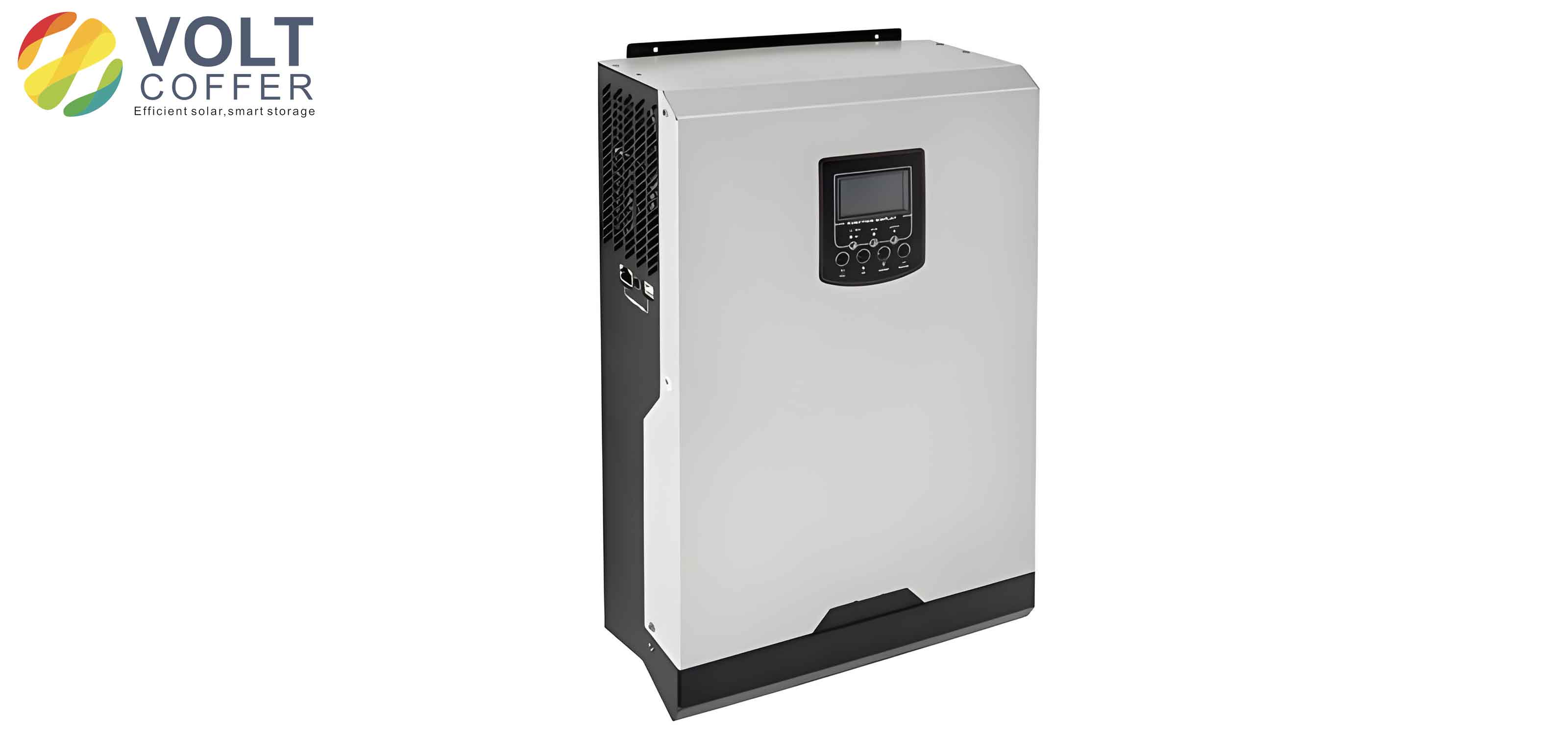
The proposed three phase inverter topology is composed of three independent single-phase H5 inverter circuits, each integrated with a flying capacitor. This structure ensures that each phase operates autonomously, minimizing interference and simplifying control. The key innovation lies in the direct connection of the PV panel’s negative terminal to the ground wire, which effectively shorts the parasitic capacitance to ground, thereby eliminating leakage current entirely. This three phase inverter configuration is depicted in the following figure, which illustrates the circuit layout and component arrangement. The flying capacitors play a critical role in energy transfer during switching cycles, enabling efficient power conversion. By decoupling the phases, this three phase inverter can handle unbalanced loads seamlessly, making it suitable for real-world applications where load asymmetry is common. The modular design also facilitates scalability and maintenance, as each phase can be addressed individually without affecting the overall system performance.
To understand the leakage current suppression mechanism, it is essential to analyze the common-mode behavior of the three phase inverter. The common-mode voltage for a single-phase non-isolated inverter can be defined as the average of the voltages between the output terminals and the ground. For the proposed three phase inverter, the total common-mode voltage is derived from the superposition of individual phase common-mode voltages. Let \( U_{CM} \) represent the common-mode voltage, and \( U_{DM} \) the differential-mode voltage. For a single phase, the common-mode voltage is given by:
$$ U_{CM} = \frac{U_{AN} + U_{BN}}{2} $$
where \( U_{AN} \) and \( U_{BN} \) are the voltages from points A and B to the neutral, respectively. In the combined three phase inverter, the total common-mode voltage \( U_{CM,total} \) is the sum of the common-mode voltages of all three phases:
$$ U_{CM,total} = \frac{U_{CM,A} + U_{CM,B} + U_{CM,C}}{3} $$
By maintaining a constant total common-mode voltage, the leakage current, which is driven by variations in this voltage, is minimized. For the proposed topology, analysis shows that \( U_{CM,total} \) remains zero under all operating conditions, ensuring complete elimination of leakage current. This is achieved through the grounding strategy and the symmetric design of the three phase inverter circuits. The following table summarizes the common-mode voltage states for different operating modes of a single phase, which can be extended to the three phase system.
| Mode | Switch States (V1-V5) | Common-Mode Voltage \( U_{CM} \) |
|---|---|---|
| 1 | 1,0,1,0,1 | 0 |
| 2 | 1,0,0,0,1 | 0 |
| 3 | 0,1,0,1,0 | 0 |
| 4 | 0,0,0,1,1 | 0 |
| 5 | 0,1,0,1,0 | 0 |
| 6 | 1,0,0,1,1 | 0 |
| 7 | 1,0,1,0,1 | 0 |
| 8 | 1,0,0,1,1 | 0 |
The working principle of this three phase inverter involves eight distinct modes per phase, as outlined in the table above. Each mode corresponds to specific switch states that facilitate energy transfer from the DC source to the load, with the flying capacitor charging and discharging to maintain voltage balance. For instance, in Mode 1, switches V1, V3, and V5 are turned on, allowing the DC source to supply power to the load while charging the flying capacitor. In Mode 2, only V1 and V5 are on, enabling the inductor to freewheel and continue charging the capacitor. This cyclic operation ensures smooth output waveforms and minimizes harmonic distortion. The independence of each phase in the three phase inverter means that imbalances in one phase do not affect the others, enhancing the system’s reliability. The modulation strategy employs a unipolar SPWM scheme with synchronized carriers, which reduces switching losses and improves efficiency. This control approach is particularly effective for three phase inverters, as it allows for continuous duty cycle adjustments and seamless voltage transitions.
The design of the flying capacitor is crucial for the performance of the three phase inverter. The capacitor must store and release energy efficiently during the negative half-cycle of operation. The energy balance equation can be used to determine the appropriate capacitance value. Let \( C_{fly} \) be the flying capacitance, \( U_{dc} \) the DC input voltage, \( U_{out} \) the output voltage, \( R_{load} \) the load resistance, and \( \Delta t \) the discharge time. The energy discharged by the capacitor should approximate the energy consumed by the load:
$$ \frac{1}{2} C_{fly} (U_{dc}^2 – U_{out}^2) = \frac{U_{out}^2}{R_{load}} \Delta t $$
Given typical values, such as \( U_{dc} = 200 \, \text{V} \), \( U_{out} = 110 \, \text{V} \), \( R_{load} = 60 \, \Omega \), and \( \Delta t = 0.5 / f_{sw} \) with a switching frequency \( f_{sw} = 20 \, \text{kHz} \), we can solve for \( C_{fly} \). To ensure low voltage ripple, the capacitance should be selected such that the voltage variation does not exceed 5 V. The current during discharge \( I_{discharge} \) can be calculated as:
$$ I_{discharge} = \frac{U_{out}}{R_{load}} $$
and the capacitance required to limit voltage ripple \( \Delta U \) is:
$$ C_{fly} = \frac{I_{discharge} \Delta t}{\Delta U} $$
For example, with \( I_{discharge} = 1.82 \, \text{A} \) and \( \Delta U = 5 \, \text{V} \), \( C_{fly} \approx 25.2 \, \mu\text{F} \). In practice, a larger capacitance, such as 440 μF, is used to account for ESR losses and ensure stable operation. This design consideration is vital for the three phase inverter, as it directly impacts efficiency and output quality. The following table provides a summary of key parameters for the flying capacitor design in the context of the three phase inverter.
| Parameter | Symbol | Value |
|---|---|---|
| DC Input Voltage | \( U_{dc} \) | 200 V |
| Output Voltage per Phase | \( U_{out} \) | 110 V |
| Switching Frequency | \( f_{sw} \) | 20 kHz |
| Load Resistance | \( R_{load} \) | 60 Ω |
| Discharge Current | \( I_{discharge} \) | 1.82 A |
| Calculated Capacitance | \( C_{fly} \) | 25.2 μF |
| Practical Capacitance | \( C_{fly} \) | 440 μF |
Experimental validation of the three phase inverter was conducted using a prototype with a rated output of 200 W per phase. The parameters included a DC input voltage of 200 V, output voltage of 110 V per phase, switching frequency of 20 kHz, and filtering components such as 5 mH inductors and 4.7 μF capacitors. The flying capacitors were set to 440 μF, and the parasitic capacitance to ground was modeled as 100 pF. Under full load conditions, the three phase inverter demonstrated stable output voltages and currents, with leakage current peaks measured at approximately 9 mA. This is well below the standard limit of 300 mA, confirming the effectiveness of the topology. The three phase inverter also handled asymmetric loads effectively, with leakage current remaining around 8 mA, highlighting its robustness. The output waveforms exhibited low total harmonic distortion (THD), ensuring compliance with grid connection standards. The following table summarizes the experimental results for different load conditions, emphasizing the performance of the three phase inverter.
| Load Condition | Output Voltage (V) | Output Current (A) | Leakage Current (mA) | THD (%) |
|---|---|---|---|---|
| Full Load | 110 | 1.82 | 9 | <5 |
| Asymmetric Load | 110 | Varies | 8 | <6 |
| Light Load | 110 | 0.91 | 7 | <4 |
The control strategy for the three phase inverter employs a single-voltage closed-loop SPWM scheme, which ensures output voltage stability despite input fluctuations or load changes. The modulation uses two carrier waves with different DC offsets, allowing for harmonic cancellation and smooth duty cycle transitions. This method is particularly advantageous for three phase inverters, as it simplifies implementation and enhances dynamic response. The mathematical representation of the modulation involves comparing a sinusoidal reference signal with triangular carriers. Let \( m(t) \) be the modulation signal, and \( c_1(t) \) and \( c_2(t) \) be the carrier signals. The switching logic for each phase can be derived as:
$$ \text{If } m(t) > c_1(t), \text{ turn on V1 and V3} $$
$$ \text{If } m(t) < c_2(t), \text{ turn on V2 and V4} $$
This ensures that the output voltage follows the reference accurately. The decoupled control of each phase in the three phase inverter allows for independent adjustment, further improving performance under unbalanced conditions. The use of SPWM in this three phase inverter reduces electromagnetic interference and switching losses, contributing to overall efficiency.
In conclusion, the proposed three phase inverter topology with flying capacitors offers a compelling solution for leakage current elimination in non-isolated PV systems. By grounding the PV negative terminal and employing independent phase control, this three phase inverter achieves complete leakage current suppression and excellent asymmetric load capability. The design principles, including flying capacitor selection and SPWM control, have been validated through theoretical analysis and experimental results. The three phase inverter prototype demonstrated low leakage current, high efficiency, and robust performance, making it suitable for practical applications. Future work could focus on optimizing the three phase inverter for higher power levels and integrating advanced monitoring features. Overall, this three phase inverter represents a significant advancement in power electronics, addressing key challenges in renewable energy systems.
Further considerations for the three phase inverter include thermal management and scalability. The switching devices in the three phase inverter must be rated for high-frequency operation to minimize losses. Heat sinks and cooling systems can be incorporated to dissipate heat generated during switching. Additionally, the modular nature of the three phase inverter allows for parallel operation of multiple units, enabling power scaling for larger installations. The control algorithm can be enhanced with digital signal processors (DSPs) for real-time adjustment and fault detection. These improvements would further solidify the three phase inverter as a versatile and reliable solution for modern energy needs. The continuous development of three phase inverter technologies is essential for advancing grid integration of renewable sources, and this topology contributes to that goal by providing a safe and efficient option.
The mathematical modeling of the three phase inverter can be extended to include dynamic behavior under transient conditions. The state-space equations for the inverter can be derived to analyze stability and response time. Let \( i_L \) represent the inductor current, \( v_C \) the capacitor voltage, and \( u \) the input voltage. The state equations for a single phase are:
$$ \frac{di_L}{dt} = \frac{1}{L} (u – v_C – i_L R) $$
$$ \frac{dv_C}{dt} = \frac{1}{C} (i_L – i_{load}) $$
where \( R \) is the resistance, and \( i_{load} \) is the load current. For the three phase inverter, these equations can be coupled through the common-mode voltage, but in this topology, the decoupling simplifies the analysis. The eigenvalues of the system matrix determine stability, and by designing the control loop properly, the three phase inverter can maintain stability under various operating conditions. This analytical approach ensures that the three phase inverter meets performance standards and operates reliably in diverse environments.
In summary, the three phase inverter discussed herein represents a innovative approach to addressing leakage current and load asymmetry issues. Through careful design and validation, it proves to be a practical and efficient solution for photovoltaic and other applications. The repeated emphasis on the three phase inverter throughout this article underscores its importance in the evolution of power conversion technologies. As the demand for clean energy grows, such advancements in three phase inverter design will play a pivotal role in shaping the future of electrical systems.