
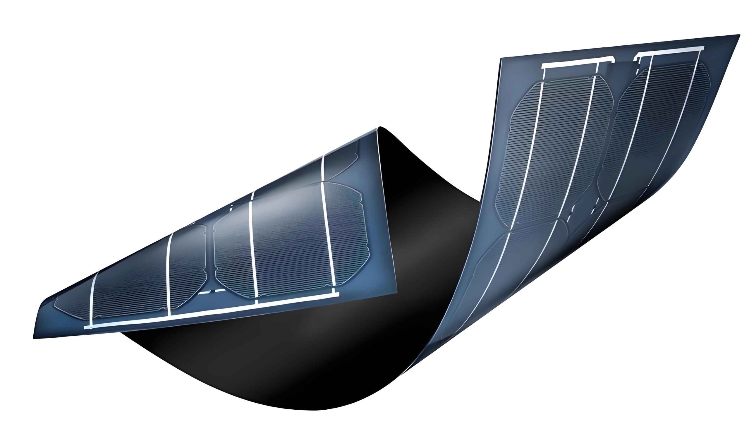
The quest for sustainable and ubiquitous solar energy conversion has driven relentless innovation in photovoltaic technologies. Among these, thin film solar panels represent a pivotal direction, promising advantages such as reduced material usage, lightweight flexibility, and compatibility with large-area, low-cost manufacturing processes. However, a persistent challenge in the fabrication of high-performance organic and perovskite-based thin film solar panels lies in the development of scalable deposition techniques that can produce layers with exceptional uniformity, controlled morphology, and minimal thickness variation over vast areas. Conventional roll-to-roll (R2R) methods, such as blade coating or slot-die coating, often struggle with slow film formation kinetics and are prone to defects like agglomeration or non-uniform crystallization when processing high-concentration solutions, ultimately compromising the device’s efficiency and reproducibility.
This discourse presents a comprehensive exploration of a novel hybrid manufacturing framework that synergistically integrates the principles of additive manufacturing (3D printing) with the precision of electrospray (ES) deposition. The core objective is to conceptualize and detail a scalable R2R apparatus designed specifically to overcome the thickness uniformity hurdle, thereby enabling the production of superior thin film solar panels. This paradigm shift hinges on leveraging electrohydrodynamic atomization to generate monodisperse, nano-scale droplets of functional inks, which are then directed onto a moving substrate within a precisely controlled 3D printing workflow. The resultant device architecture promises unprecedented control over film topography, paving the way for thinner, more uniform, and highly efficient photovoltaic layers.
Technological Foundations: Electrospray and Additive Principles
The proposed methodology is built upon two foundational pillars: electrospray technology for droplet generation and additive manufacturing principles for system control and path planning.
Electrospray Deposition Fundamentals
Electrospray is a versatile electrohydrodynamic process where a liquid jet emanating from a capillary nozzle is atomized into a fine aerosol of charged droplets under the influence of a strong electric field. For thin film solar panel fabrication, the “ink” typically consists of a solution containing the active layer materials (e.g., polymer donors, fullerene or non-fullerene acceptors, perovskite precursors) dissolved in a volatile solvent.
The process initiates when a high voltage (typically in the range of 5-30 kV) is applied between the metallic nozzle (connected to the high-voltage supply) and a grounded conductive collector substrate. The electric field induces charge accumulation at the liquid meniscus, transforming it into a conical shape known as a Taylor cone. Beyond a critical voltage, the electrostatic repulsion overcomes the liquid’s surface tension, and a fine jet erupts from the cone’s apex. This jet subsequently breaks up into a plume of highly charged, micron- or nano-sized droplets. The governing force balance at the onset of jetting can be described by a simplified form of the Taylor criterion:
$$ \gamma \frac{2}{R} \approx \frac{\epsilon_0 E^2}{2} $$
where $\gamma$ is the surface tension of the liquid, $R$ is the radius of curvature of the meniscus, $\epsilon_0$ is the permittivity of free space, and $E$ is the applied electric field strength at the tip.
These charged droplets undergo Coulombic fission and rapid solvent evaporation as they travel towards the collector. By the time they reach the substrate, they are often solid particles or highly concentrated precursor deposits. The key advantages for thin film solar panel fabrication are manifold:
- Ultra-thin, Uniform Films: The Coulombic repulsion between identically charged droplets prevents coalescence during flight and promotes a even spatial distribution upon impact, leading to exceptionally smooth and pinhole-free layers.
- Non-Contact Deposition: The process does not require physical contact with the substrate, making it ideal for delicate or pre-patterned surfaces.
- High Material Utilization: Nearly 100% of the sprayed material can be directed onto the substrate, minimizing waste.
- Nanoscale Control: Droplet size can be precisely tuned by adjusting solution properties (viscosity, conductivity, surface tension) and process parameters (flow rate, applied voltage), allowing for control over film nanostructure.
Integration with 3D Printing Philosophy
3D printing, or additive manufacturing, introduces a layer-by-layer, digitally controlled fabrication philosophy. Integrating this with electrospray translates into precise robotic control over the deposition source (the electrospray printhead) relative to the substrate. The system operates based on a pre-defined digital toolpath, enabling:
- Patterned and Gradient Deposition: Beyond uniform layers, the printhead can trace complex paths to create patterned active layers or deposit compositional gradients across the substrate, potentially for tandem cell architectures or integrated electronics.
- Multi-Material Printing: Multiple independent electrospray printheads, each containing a different functional ink (e.g., electron transport layer, active layer, hole transport layer), can be integrated into a single platform. This allows for the sequential, in-line deposition of all layers required for a complete thin film solar panel device structure.
- Dynamic Parameter Control: Printing parameters such as printhead velocity, stand-off distance, and even voltage can be dynamically varied along the toolpath to locally modulate film properties.
- Scalability through R2R Integration: The digitally controlled, multi-axis motion system seamlessly integrates with a continuous R2R substrate handling system. The substrate unwinds from a feed roller, passes under the deposition zone where the electrospray printhead(s) execute their toolpath, and is subsequently rewound, enabling endless, large-scale production.
System Architecture and Operational Principles
The envisioned R2R apparatus for manufacturing thin film solar panels is a sophisticated synthesis of electrostatic deposition, precision motion control, and web handling. The core components and their interplay are detailed below.
Core Components and Configuration
The system’s layout is designed for continuous, uniform coating of flexible substrates. The primary subsystems include:
- High-Voltage Power Supply (HVPS): A stable, programmable DC power supply capable of delivering up to 30-50 kV. Its positive terminal is connected to the electrospray nozzle(s), while its negative terminal is connected to a grounded collection assembly.
- Electrospray Printhead Assembly: This consists of one or more syringe pumps for precise ink delivery, associated fluidic lines, and metallic nozzles (e.g., stainless steel hypodermic needles). The printhead is mounted on a multi-axis motion system.
- Grounded Collector & R2R Web Platform: A conductive base plate (collector) forms the grounded counter-electrode. Mounted on this base is the R2R mechanism, comprising an unwinding roller, a rewinding roller, and a precision motorized conveyor system that transports the substrate. The substrate itself must be either conductive (e.g., Indium Tin Oxide-coated PET) or be backed by a conductive carrier film.
- Substrate Flattening and Tensioning System: Critical for uniformity, this involves a series of idler rollers and, most importantly, dedicated flattening rollers positioned immediately before and after the deposition zone. These rollers, often made of conductive rubber or coated metal, ensure the substrate is perfectly flat and taut under the printhead, eliminating wrinkles or air gaps that could disrupt the electric field or cause shadowing.
- Multi-Axis Motion System: Typically a gantry-style or robotic arm system that provides precise X-Y-Z control of the electrospray printhead. This allows the nozzle to scan across the width (X-axis) of the moving web (Y-axis direction) and maintain an optimal stand-off distance (Z-axis).
- Environmental Enclosure (Optional but Recommended): A chamber to control ambient conditions (temperature, humidity, inert gas atmosphere) which is crucial for processing air-sensitive materials like perovskites or certain organic semiconductors.
The fundamental operational principle involves establishing a stable electrospray plume from the printhead towards the grounded, moving substrate. The charged droplets are attracted to the substrate, forming a dense, uniform coating. The printhead’s transverse motion (perpendicular to web travel) ensures full coverage across the substrate’s width, while the web’s continuous movement enables the deposition of an endless film. The synchronized motion of the web and the printhead is governed by a central control system.
Mathematical Modeling of Deposition Uniformity
The thickness profile of the deposited layer for a thin film solar panel is a critical metric. It can be modeled by considering the deposition rate and the relative motion of the printhead. For a single printhead moving back and forth across a web moving at constant speed, the local film thickness $d(x,y)$ at a point on the substrate can be approximated by integrating the contribution of the spray flux over time.
Assuming a Gaussian spray flux distribution $F(r)$ from the nozzle with a characteristic deposition radius $\sigma$:
$$ F(r) = \frac{Q}{\pi \sigma^2} e^{-r^2 / \sigma^2} $$
where $Q$ is the total mass deposition rate (mass/time) and $r$ is the radial distance from the spray axis. The contribution to thickness at substrate coordinate $(x_0, y_0)$ depends on the trajectory of the printhead $(X(t), Y(t))$ relative to the moving web. If the web moves with velocity $v_{web}$ in the y-direction, and the printhead scans in the x-direction with a velocity profile $v_{head}(t)$, the effective relative position is $(x_0 – X(t), y_0 – Y(t) + v_{web}t)$. The resulting thickness is proportional to the time integral of the flux over the deposition period $T$:
$$ d(x_0, y_0) \propto \int_{0}^{T} F\left( \sqrt{(x_0 – X(t))^2 + (y_0 – Y(t) + v_{web}t)^2} \right) dt $$
Optimizing $X(t)$ and $v_{head}(t)$ (e.g., using a constant velocity bi-directional scan) is essential to minimize thickness variation, a key goal for high-performance thin film solar panels. This model highlights the digital control advantage: the toolpath $X(t)$ can be optimized computationally to achieve a desired thickness profile.
| Technique | Principle | Advantages | Disadvantages for Thin Film Solar Panels | Typical Film Uniformity |
|---|---|---|---|---|
| Spin Coating | Centrifugal force spreading | Excellent lab-scale uniformity, simple setup. | Extremely low material efficiency (<5%), not scalable, limited to small, rigid substrates. | Excellent (on small area) |
| Blade / Doctor Blade Coating | Mechanical shearing and evaporation | Scalable (R2R compatible), relatively simple. | Prone to “coffee-ring” effect, thickness depends on solution viscosity and evaporation rate, can cause molecular alignment. | Moderate to Good |
| Slot-Die Coating | Precise metering through a die head | Excellent thickness control, high uniformity, R2R compatible. | High-precision engineering required, sensitive to ink rheology, difficult for very low viscosity inks. | Very Good |
| Inkjet Printing | Drop-on-demand piezoelectric actuation | Digital patterning, non-contact, efficient material use. | Limited by ink viscosity, satellite drops can cause defects, relatively slow for full-area coverage. | Good (patterned) |
| Electrospray (Proposed Hybrid) | Electrohydrodynamic atomization | Ultra-thin & uniform films, high material efficiency, non-contact, compatible with sensitive materials, scalable via R2R. | Requires conductive or grounded substrate, parameter optimization can be complex, potential for airborne particles. | Excellent (Target) |
Process Optimization for Thin Film Solar Panel Fabrication
The performance of the final thin film solar panel is acutely sensitive to the morphological and electronic properties of each deposited layer. The hybrid 3D printing-electrospray system offers numerous levers for optimization, which can be categorized into ink formulation, electrospray process parameters, and motion/thermal parameters.
Ink Formulation and Rheology
The functional ink must satisfy dual constraints: it must be an optimal formulation for the photovoltaic material system and be suitable for stable electrospray operation. Key parameters include:
- Solvent System: A balance between volatility (for rapid droplet drying) and boiling point (to prevent clogging at the nozzle). Mixtures like Chlorobenzene/Dichlorobenzene for organics or DMF/DMSO for perovskites are common. The solvent’s dielectric constant and conductivity also significantly influence jet stability.
- Solution Concentration and Viscosity: Concentration directly impacts final film thickness and phase separation morphology in bulk heterojunction thin film solar panels. Viscosity ($\eta$) affects the jetting mode; typically, a viscosity in the range of 1-100 cP is suitable for stable cone-jet electrospray. The relationship often involves the dimensionless Ohnesorge number ($Oh = \frac{\eta}{\sqrt{\rho \gamma L}}$), where $\rho$ is density and $L$ a characteristic length.
- Electrical Conductivity ($K$): This is critical for charge transport within the liquid and establishing a stable Taylor cone. Optimal conductivity usually falls between $10^{-4}$ and $10^{-1}$ S/m. Additives like ionic liquids can be used to tune conductivity without adversely affecting solar cell performance.
Electrospray Process Parameters
These parameters govern the transition from a liquid stream to a fine, charged aerosol and ultimately define the droplet impact conditions on the substrate for the thin film solar panel layer.
| Parameter | Typical Range | Primary Influence | Effect on Thin Film Solar Panel Layer |
|---|---|---|---|
| Applied Voltage (V) | 5 – 30 kV | Electric field strength, determines jet initiation and droplet charge. | Higher voltage leads to smaller droplets, finer film grain structure, but may cause electrical breakdown or arcing. |
| Flow Rate (Q) | 0.1 – 10 mL/hr | Mass delivery rate to the Taylor cone. | Directly scales deposition rate and final film thickness. Too high a flow leads to unstable dripping; too low leads to intermittent spray. |
| Stand-off Distance (H) | 5 – 20 cm | Droplet flight time and solvent evaporation extent. | Longer distance allows more complete solvent evaporation, leading to drier particle impact, which can reduce film roughness but may decrease adhesion. |
| Nozzle Inner Diameter | 0.1 – 0.5 mm | Initial jet diameter and hydraulic resistance. | Smaller diameters facilitate finer droplets but are more prone to clogging and require higher pressure or lower viscosity. |
The stable operational window is often mapped on a regime diagram, with applied voltage versus flow rate being the most common. The goal is to operate in the “cone-jet” mode, which produces a monodisperse droplet distribution essential for uniform thin film solar panel active layers.
Motion and Thermal Control Parameters
Integration with the 3D printing/R2R framework introduces another layer of control variables:
- Printhead Scan Speed ($v_{head}$): Must be synchronized with the web speed ($v_{web}$) and the deposition flux to achieve the target thickness per pass. A slower scan speed or multiple passes increase local thickness.
- Substrate Temperature ($T_s$): Controlled via a heated collector plate. Elevated temperatures promote solvent evaporation upon impact, slowing layer-by-layer “welding” of deposited nanoparticles and influencing crystallization kinetics in the thin film solar panel active layer.
- Overlap and Toolpath Strategy: The percentage overlap between successive scan lines determines microscopic uniformity. A digitally controlled toolpath can also implement non-raster patterns (e.g., Hilbert curves) to minimize directional artifacts.
The interplay of these parameters defines a complex optimization landscape. The final film thickness ($d_f$) for a single material can be estimated from the mass balance:
$$ d_f = \frac{Q \cdot C \cdot t_{dep}}{A \cdot \rho} $$
where $Q$ is the flow rate, $C$ is the solid concentration in the ink, $t_{dep}$ is the total deposition time per unit area (a function of $v_{head}$, $v_{web}$, and number of passes), $A$ is the deposition area, and $\rho$ is the density of the solid film. For the multi-layer structure of a complete thin film solar panel, this equation is applied sequentially for each functional layer (ETL, active layer, HTL, etc.).
Advantages, Potential Applications, and Future Outlook
The hybrid 3D printing-electrospray R2R platform is not merely an incremental improvement but a transformative approach with distinct advantages for the future of thin film photovoltaics.
Key Advantages of the Hybrid Approach
- Superior Morphological Control: The ability to deposit from nano-droplets results in extremely smooth, dense, and pinhole-free films. This minimizes shunt paths and improves the interfacial contact area in the thin film solar panel, directly enhancing fill factor and open-circuit voltage.
- Digital and Flexible Manufacturing: The process is inherently digital. Changing the design or toolpath requires only software modifications, enabling rapid prototyping of new thin film solar panel architectures (e.g., graded heterojunctions, micro-patterned cells) and easy scale-up.
- Material and Cost Efficiency: High material utilization (>90%) reduces raw material costs. The non-contact nature minimizes substrate damage and contamination.
- Compatibility with Sensitive and Novel Materials: The gentle, solvent-free (by the time of impact) deposition is ideal for air-sensitive materials like perovskite precursors or delicate organic molecules that might degrade under the shear forces of blade coating.
- True R2R Scalability for Large-Area Production: The system design is fundamentally aligned with continuous manufacturing, addressing the core challenge of moving high-efficiency thin film solar panel technologies from the lab to the gigawatt production scale.
Broader Applications and Impact
While focused on thin film solar panels, the technological platform has profound implications across functional film manufacturing:
- Perovskite Solar Modules: The gentle deposition could enable high-speed, uniform coating of large-area perovskite layers without the detrimental effects of shear-induced crystallization.
- Flexible and Wearable Electronics: The ability to print uniform films on flexible plastic substrates like PET or PEN is perfect for creating lightweight, bendable thin film solar panels for integration into buildings, vehicles, or portable devices.
- Multi-Functional Coatings: The same principle can deposit layers for organic light-emitting diodes (OLEDs), sensors, thin-film batteries, and anti-reflective or hydrophobic coatings.
- Barrier Films and Encapsulation: Electrospray can create ultra-uniform, defect-free polymer or hybrid barrier layers essential for encapsulating moisture-sensitive thin film solar panels to ensure long-term operational stability.
Future Directions and Challenges
The path to industrialization involves addressing several research and engineering frontiers:
- High-Throughput Multi-Nozzle Systems: Developing arrays of stable, independently addressable electrospray nozzles to drastically increase deposition area rate, moving from a single scanning printhead to a wide, stationary print bar.
- Advanced In-Situ Monitoring and Control: Integrating real-time diagnostics such as high-speed imaging for jet monitoring, laser diffraction for droplet size analysis, and spectroscopic ellipsometry for thickness measurement. This data can feed back to adjust parameters dynamically, enabling closed-loop control for flawless thin film solar panel production.
- Modeling and Digital Twin Development: Creating comprehensive multi-physics models that couple fluid dynamics, electrostatics, mass transfer, and film formation. A digital twin of the process would allow for virtual optimization of parameters and toolpaths before physical trials, accelerating development cycles.
- Integration with Other Printing Techniques: Combining the electrospray station with other inline processes, such as slot-die coating for charge transport layers or screen printing for electrodes, to create a fully integrated, sequential R2R production line for complete thin film solar panel modules.
In conclusion, the convergence of 3D printing’s digital flexibility with electrospray’s precision deposition capability presents a compelling and powerful manufacturing paradigm. This hybrid approach directly targets the most stringent requirements for next-generation thin film solar panels: nanoscale uniformity over macroscopic areas, minimal material waste, and compatibility with high-volume roll-to-roll production. By providing an engineered solution to the historical challenge of thickness variation, this technology holds the key to unlocking the true commercial potential of organic, perovskite, and other emerging thin film photovoltaic technologies. Its successful implementation will not only elevate the performance and reduce the cost of thin film solar panels but also establish a versatile platform that will catalyze innovation across the broader landscape of advanced functional coatings and flexible electronics, contributing significantly to a sustainable energy future.