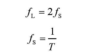
1. Basic principles of DC/DC conversion
DC/DC converter, also known as DC Chopper, is an electrical energy conversion device that converts a fixed DC power source into an adjustable DC power source. There are various types of DC choppers, among which two types of circuits are the most basic: buck circuit and boost circuit.
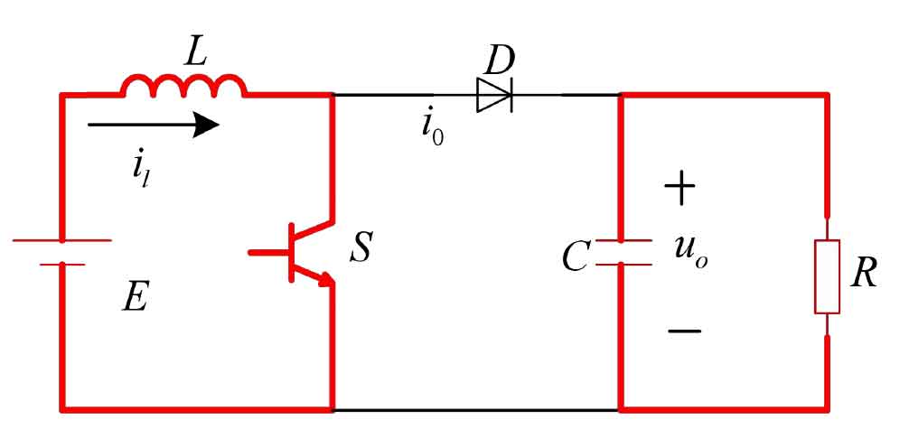
(1) Buck conversion circuit:
Figure 1 shows the topology of the buck converter circuit, which is a series switching circuit, also known as a buck converter circuit. The average output voltage oU is always lower than the input voltage Uin. The operation of the Buck chopper circuit is related to the conduction of the power switch tube and diode. When the power switch tube is in the open state, when the power supply E supplies power to the load LR, diode D bears the reverse voltage to turn off. Under the action of the inductor voltage UL=Uin Uo, the load current oi increases exponentially, and the stored energy of inductor L increases. When the power switch S is disconnected, the load current continues to flow through diode D, the inductor releases the previously stored energy, and the inductor current decreases exponentially. In order to make the load LR current continuous and minimize pulsation, the series inductance L value is usually kept as large as possible.
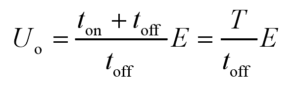
When the current is continuous, the load terminal voltage is:
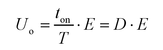
Among them, the conduction duty cycle D is:
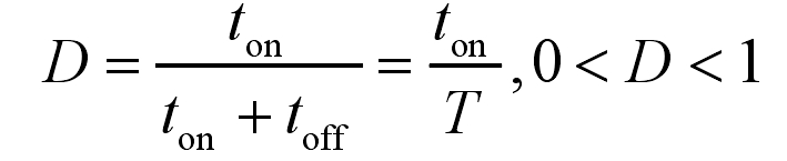
Among them, ton is the time when VT conducts; Toff is the time when VT is turned off.
Because D ≤ 1, the maximum oU is E, reducing the duty cycle D leads to a decrease in Uo, so Buck has the function of voltage reduction and chopping.
In order to achieve the goal of adjustable output voltage, it is necessary to control the duty cycle of the chopping circuit, which can be summarized into the following three implementation methods:
1) Pulse width modulation (PWM): The period T remains unchanged, adjust ton.
2) Frequency modulation: Ton remains unchanged, changing the period T.
3) Hybrid modulation: both ton and T are adjustable, changing the duty cycle.
(2) Boost converter circuit
Figure 2a) shows the topology of the Boost converter circuit, which belongs to a parallel switching circuit, also known as a boost converter.
The average output DC voltage of the boost chopper circuit is greater than the input DC voltage of the power supply, so it is called a boost converter circuit. Assuming the device is in an ideal state, when the power switch S is turned on, the input current 1i flows through inductor L, and the current i1 in inductor L increases exponentially. Diode D is cut off in reverse, with a current io of 0. The DC power supply stores energy in inductor L. The current at the load end is maintained by capacitor C. Due to the large value of C, the output voltage ou is considered constant, denoted as Uo. Let the time when S is connected be ton, and the energy accumulated on L during this stage is EI1 ton. The current path is shown in red in Figure 3.
When switch S is disconnected, power supply E and inductor L simultaneously provide energy to capacitor C and load R, and capacitor C transitions from discharge state to charging state. When the S disconnection time is set to toff, the energy released by inductor L during this period is (UO-E) I1toff. In a stable state, the accumulated energy and released energy of L in one cycle T are equal. Its output voltage is:
In the formula, T/toff is greater than 1, so the power supply voltage E is lower than the output voltage Uo. This circuit has a boosting effect and is called a boost chopper circuit. Ttoff is called boost ratio, and changing the size of Uo is achieved by adjusting the T/toff size. The modulation method is similar to the method of changing the conductivity ratio D introduced in the previous section. The reciprocal of the boost ratio is expressed as β , Namely β= Toff/T, then there is D+ β = 1.
Therefore, the voltage expression of the Boost circuit becomes:
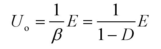
It can be seen that the average output voltage oU of the circuit is greater than the input DC voltage of the power supply, and the chopper circuit has a boost function. The reason why the boost chopper circuit causes the output voltage oU to be higher than the power supply voltage E can be attributed to two points: firstly, after energy storage, L has the effect of causing a sudden increase in voltage; The second is the existence of capacitor C that can maintain stable output voltage.
2. Single inductor Boost converter
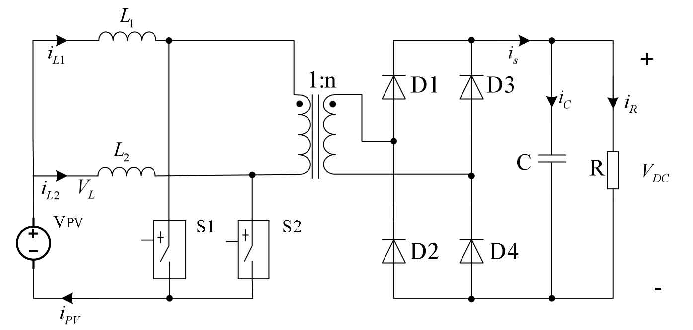
Single inductor Boost push-pull converter circuit (SIC):
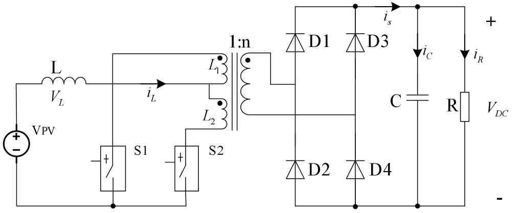
From Figure 4, it can be seen that the boost part of this circuit is implemented by a push-pull conversion circuit. The converter consists of switch tube S1, switch tube S2, and a transformer, where the center tap of the transformer divides it into two parts: L1 and L2. When two forward converters work, the phase difference is 180 degrees, and the energy is alternately transferred to the subsequent load, which is called push-pull transformation.
Due to the lack of isolation between the emitter of power switch S1 and switch S2 and the negative pole of the power supply, the driving circuit of this converter has the following advantages: it is very convenient and simple to drive, and can be directly driven without electrical isolation. This topology structure is compact, the driving circuit is simple, and the boosting effect is obvious.
The specific working process of boost conversion can be summarized into three modes:
Mode 1: S1 and S2 conduct, inductors L1 and L2 charge, transformer input voltage is 0, and capacitor C discharges to the load;
Mode 2: S1 turns off, S2 conducts, inductor L1 discharges, L2 charges, transformer input is positive voltage, rectified by D1 and D4, to charge the capacitor and supply power to the load;
Mode 3: S1 conducts, S2 turns off, inductor L1 charges and L2 discharges, transformer input is negative voltage, rectified by D2 and D3, to charge the capacitor and supply power to the load.
During the working process, the duty cycle of the driving signals for S1 and S2 is set to 50%, and the DC voltage is converted into AC voltage through the push-pull conversion circuit formed by the converter. The function of a high-frequency transformer is to increase the voltage and transfer electrical energy to the secondary side. Using four bipolar D1-D4 for rectification, high-frequency AC is rectified into DC. During operation, the current only flows through one of the switching devices, which is helpful in reducing the conduction loss of the converter, improving its conversion efficiency, and reducing its size.
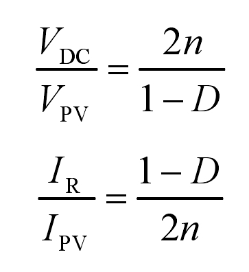
Therefore, the output voltage and current of the SIC converter can be calculated as follows:
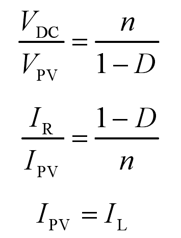
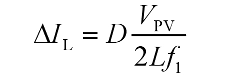
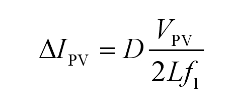
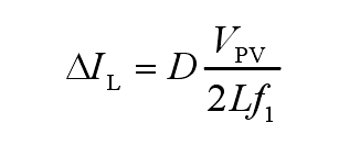
Among them: D is the modulation ratio. The input current ripple is:
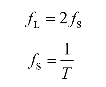
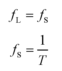
The frequency of inductive current is:
Through analysis, the following conclusion can be drawn: The circuit adopts a Boost boost circuit and a push-pull boost circuit, and by combining the two boost circuits to increase the input voltage, the overall boost efficiency is greatly improved. However, its main drawback is that the main part of the circuit still uses a hard switching circuit, which causes significant switching losses and limits the efficiency of the converter to a certain extent. Therefore, it is necessary to improve the converter circuit, and a series resonant soft switching technology can be introduced into push-pull Boost converters to solve this problem.
3. Dual inductance Boost converter
The dual inductor Boost push-pull converter circuit (DIC) is shown in Figure 5:
Switching mode:
Mode 1: S1 and S2 conduct, inductors L1 and L2 charge, transformer input voltage is 0, and capacitor C discharges to the load;
Mode 2: S1 turns off, S2 conducts, inductor L1 discharges, L2 charges, transformer input is positive voltage, rectified by D1 and D4, to charge the capacitor and supply power to the load;
Mode 3: S1 conducts, S2 turns off, inductor L1 charges and L2 discharges, transformer input is negative voltage, rectified by D2 and D3, to charge the capacitor and supply power to the load.
Among them: D is the modulation ratio.
The input current ripple is:
The frequency of inductive current is:
The main advantage of a converter with this topology is that compared to traditional Boost converters, the inductance is reduced by half; Reduce the current level of the switching tube by half; Significantly reduces the harmonic of input current; Can effectively solve the current surge problem during diode reverse recovery; The output DC filter circuit is simplified, and the quality of the DC output is improved.
4. Full bridge Boost converter
The commutation mode is shown in Figure 6:
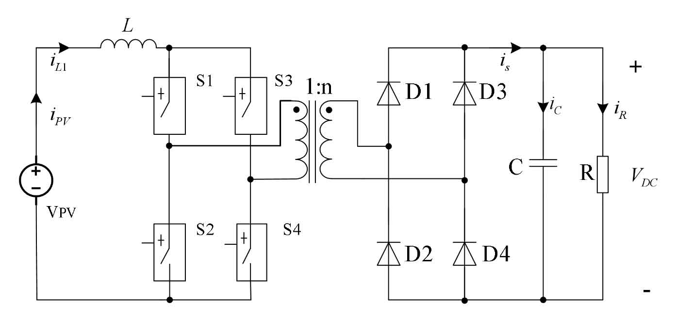
Mode 1: S1, S2, S3, and S4 conduct, inductor L charges, transformer input voltage is 0, and capacitor C discharges to the load;
Mode 2: S1 and S4 conduct, S2 and S3 turn off, the input voltage of the transformer is positive, rectified by D1 and D4, to charge the capacitor and supply power to the load;
Mode 3: S1 and S4 turn off, S2 and S3 conduct, the input voltage of the transformer is negative, rectified by D2 and D3, to charge the capacitor and supply power to the load.
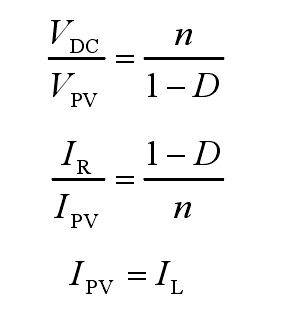
Among them: D is the modulation ratio:
The input current ripple is:
The frequency of inductive current is: