
1. Overall Function and Main Technical Division
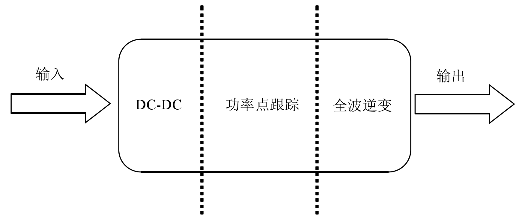
A solar inverter is an energy conversion device that converts solar energy into alternating current. The solar energy is collected and converted into direct current by the photovoltaic array, which is input to the input end of the solar inverter. It is then converted into power frequency 220V AC power output through steps such as boosting, half wave conversion, rectification, synchronization, and phase matching. According to its functional division, it can be divided into three parts, namely the DC-DC part, power point tracking part, and full wave inverter part, as shown in Figure 1.
The DC-DC link is the process of converting continuous direct current through high-frequency MOSFETs into discontinuous direct current. In this process, the high-frequency MOSFET adopts sine pulse width modulation (SPWM) to ensure that the conduction time of the MOSFET follows a sinusoidal distribution and outputs half a wave to the next stage. The designed solar inverter is a dual channel alternating solar inverter, where the upper and lower channels each generate half waves. When the upper and lower power transistors work alternately, a continuous half wave waveform is displayed at the output end of the flyback transformer.
The main related technologies involved in the DC-DC process include the conversion of continuous DC voltage to intermittent AC voltage, SPWM modulation, and soft switching algorithms. The main technical issues that exist include SPWM wave modulation not meeting the sine variation rule, insignificant soft switching algorithm effect, energy loss during the conduction and turn off process of power switching tubes, and the design of leakage inductance energy absorption circuits.
The maximum power point tracking technology adjusts the matching input and load impedance to place the output power point of the solar inverter at the current maximum output power point, achieving efficient and stable output of the solar inverter. If this control algorithm is not implemented, the output voltage of the solar inverter will not be stable, and the power point will quickly swing around the maximum power point. At this time, it is extremely easy to generate peak voltage, breakdown power switch tubes, and cause serious impact on the end appliances, bringing safety hazards and wasting most of the energy. At present, the maximum efficiency of MPPT internationally is about 99.9%.
The main related technologies involved in the maximum power point tracking section include MPPT control strategy, absorption and reuse of leakage inductance energy, and peak voltage suppression technology. The main technical issues that exist include the stability and efficiency of the MPPT control algorithm, the derivation and implementation of the theoretical model of the MPPT control algorithm, leakage inductance energy, and the back impact of voltage spikes caused by various reasons on the power switch tube, as well as the energy consumption caused by them, and the improvement of the efficiency of the solar inverter.
The full wave inverter part is to convert the alternating half wave waveform generated by the upper and lower circuits of the front half of the solar inverter into a 50Hz sine wave by rectifying two reverse PWM waves to complete the output of the solar inverter. In the process of full wave inversion, in order to prevent conflicts between the two reverse PWM waves, which may cause breakdown and damage to the MOSFETs on the upper and lower channels of the H-bridge, there needs to be a delay time setting between the two reverse PWM waves. Due to the existence of this delay time, the full wave after inversion will experience zero point drop when crossing the zero point. The designed solar inverter is set with a delay time of 90ns based on the selected MOS reaction time and experimental results.
The relevant technologies involved in the full wave inversion section include phase shift correction technology, zero drop correction technology, and zero crossing detection technology. The main technical issues that exist include the synchronization correlation between half wave generation and full wave inversion, alternating half wave phase shift, zero drop of full wave inversion, output type sine wave, timeliness of zero crossing detection, and the formulation and implementation of synchronous inversion strategies combining software algorithms and hardware circuits.
2. SPWM wave modulation design scheme
Sinusoidal Pulse Width Modulation, abbreviated as SPWM. According to the theoretical idea of mathematical integration, a continuous function can be gradually approximated by an infinite number of discrete functions. For the sine half wave that needs to be output in the DC-DC process, it can be replaced by an infinite number of rectangular pulses of equal width but different amplitudes. In each small time period, the area of the rectangular pulse is infinitely close to the area enclosed by the sine wave in that time period. In continuous time, all rectangular wave areas will infinitely approximate the area of a sine wave. According to the principle of integration, the two can be considered equal in continuous time. Among them, the width of the rectangular pulse is determined by the duty cycle of the power switching tube. In order to output a sine half wave, the amplitude of each rectangular pulse needs to follow the law of sine half wave variation. However, for high-frequency power devices, controlling the adjustable duty cycle to control the output power and match the input and output impedance is much more convenient, fast, and practical than adjusting the output amplitude with a fixed duty cycle. So, if infinitely many rectangular pulses of equal width and unequal amplitude are replaced by the same number of rectangular pulses of equal amplitude and unequal width, and the area of each corresponding rectangular pulse is equal at each moment, then as long as the duty cycle of each rectangular pulse satisfies the waveform change law of a sine half wave after sampling according to Nyquist’s theorem, The area of the infinite number of rectangular pulses with equal amplitude and unequal width to be replaced is also equivalent to the area enclosed by the sine half wave, and its output can also be equivalent to a sine wave. This is the design principle of SPWM modulation.
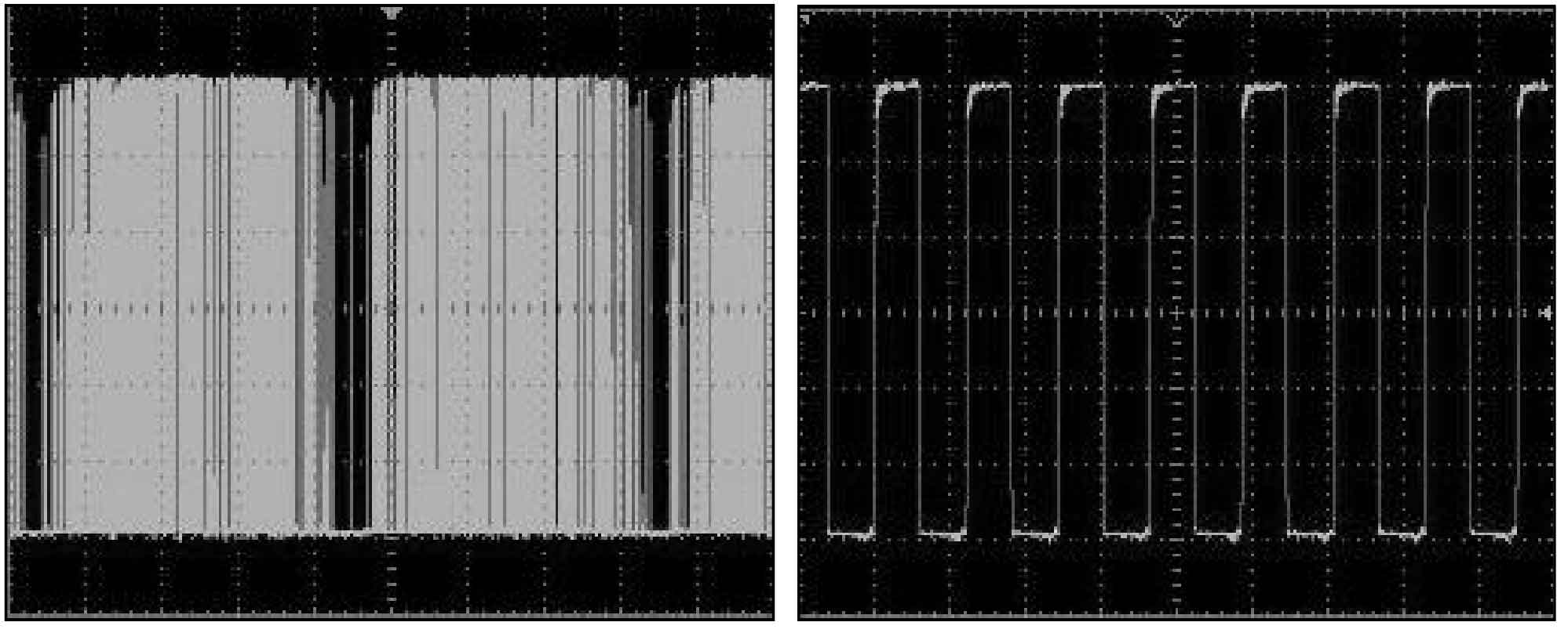
For the SPWM modulation technology with equal amplitude and adjustable duty cycle, the SPWM modulation wave can be obtained by comparing sine waves and triangular waves. However, this method greatly complicates the circuit topology of solar inverters and increases the design cost of solar inverters. Based on this, in the grid connected solar micro inverter designed in this article, the efficient calculation function and sampling accuracy of the 8-channel 12 bit analog-to-digital converter built-in in the DSP chip are utilized, with a sampling accuracy of 20ns. A standard sine table is defined, and the control waveform data for generating SPWM waves is obtained through algorithm and table lookup method rotation training. The measurement waveform and waveform expansion diagram of the output SPWM control wave are shown in Figure 2. One of the main reasons for using SPWM waves to control high-frequency MOSFETs is that this technology can easily achieve soft switching technology, and this control strategy has the advantages of both control and regulation.
By modulating with SPWM, the duty cycle of the high-frequency power switching transistor is controlled. The input continuous DC voltage pulse is cut into infinite intermittent DC pulses of equal height but not equal width in a table lookup rotation manner, so that the width of each rectangle meets the variation law of sine pulses. After that, the half wave rectifier diode outputs a half wave waveform.
3. Soft switching technology design scheme
The opposite of the soft switching phenomenon is the hard switching phenomenon. As shown in Figure 3, during the conduction and turn off processes of power MOSFETs, the phenomenon of overlapping voltage and current due to the slow variation characteristics of voltage and current is called hard switching phenomenon.
During the conduction process of power switching tubes, the drain source voltage decreases from high to zero and the current starts to increase from zero. As a result, a superimposed shadow area is formed between the voltage and current, forming an area that consumes power. The larger the area, the greater the power consumed, and the more energy is lost during the conduction process of the switch. Similarly, during the power transistor shutdown process, the drain source voltage increases from zero and the current decreases from high to zero, resulting in a superimposed power consumption area for both voltage and current. The phenomenon of hard switching will lead to the loss of switching energy, causing voltage spikes, current spikes, and electromagnetic interference. This phenomenon is particularly fatal for the design of solar inverters, as they use high-frequency power switching devices. The higher the frequency, the greater the loss, and the higher the peak amplitude, the more obvious the electromagnetic interference cannot be ignored. If not suppressed, the power switching tubes will quickly heat up and heat up, accompanied by a whistling sound. If the duration is too long, it will inevitably burn out the power switching tubes, and in severe cases, it may even cause permanent damage to other components in the circuit.
Soft switching technology aims to reduce energy loss and electromagnetic interference during the conduction and turn off processes of the switching tube, while preventing and avoiding voltage spikes, thereby improving the safety of solar inverters during operation. The essence of soft switching technology is to delay the change of voltage or current, so that the voltage (current) does not intersect linearly with the current (voltage) during the rise or fall, thereby maintaining the stable operation of high-frequency power switching tubes for a long time in an environment with energy loss and normal temperature. The implementation method of soft switching technology is to introduce necessary and parameter matched resonant circuits at the DC-DC stage. Through the resonance of capacitors and inductors, the speed of voltage and current changes is delayed, so that when the power switch is turned on, the drain source voltage drops from high to zero and the driving voltage starts to rise from zero, achieving zero voltage conduction (ZVS).
Due to the control of SPWM modulation waveform, the DC-DC environment outputs voltage pulses, and the soft switching resonance also outputs voltage pulses in the DC link. In order to achieve ZVS conduction of the switching tube under zero voltage conditions, the conduction time of the switching tube must be selected when the DC link resonance reaches its voltage zero. Therefore, when designing the soft switching control strategy of the solar inverter switching tube, this paper derives mathematical theoretical formulas, Collect signal data values from the calculation formula, use SPWM technology to calculate and adjust the duty cycle of the power switch in real-time. However, due to the fact that the traditional formula for calculating the duty cycle of soft switches requires real-time collection of voltage and current values in order to perform real-time calculations, which will inevitably increase the complexity of hardware circuit topology and improve the design cost of solar inverters, this article modifies and extends the traditional formula for calculating the duty cycle of soft switches with correct mathematical theory deduction. While maintaining stable output at maximum power, Simplified the topology structure of the hardware circuit and improved the inverter efficiency.
4. Design scheme for leakage sensing energy absorption
In the design of solar inverters, they can be divided into two types based on whether a transformer is needed to boost the input DC voltage: solar inverters with transformers and solar inverters without transformers [29]. For grid connected solar micro inverters, due to their high-frequency characteristics, it is necessary to isolate the DC input and AC output terminals of the solar inverter. Therefore, according to whether it has isolation characteristics, transformers can be divided into isolation transformers and non isolation transformers. In order to play a related electrical isolation role, the grid connected solar micro inverter designed in this article uses a flyback transformer as the isolation boosting element.
During the production process of isolation transformers, there will be a certain gap in the middle of the transformer [31-32], which can achieve circuit isolation between the AC and DC parts and improve the safety factor of solar inverter equipment containing transformers. However, due to the presence of magnetic leakage, the primary energy of the flyback transformer cannot be fully transmitted to the secondary end of the transformer in each power cycle. For any solar inverter containing a transformer, if the energy at the primary end is limited, subtracting the energy that cannot be transmitted will result in insufficient energy at the secondary output end of the transformer, causing distortion of some waveforms or inability of the main components to function properly, especially at the half wave connection. Due to energy loss, the waveform at the half wave connection will experience jitter and distortion. When the power is insufficient, The half wave waveform will exhibit a sharp peak at the peak, which seriously affects the subsequent inversion operation of the solar inverter.
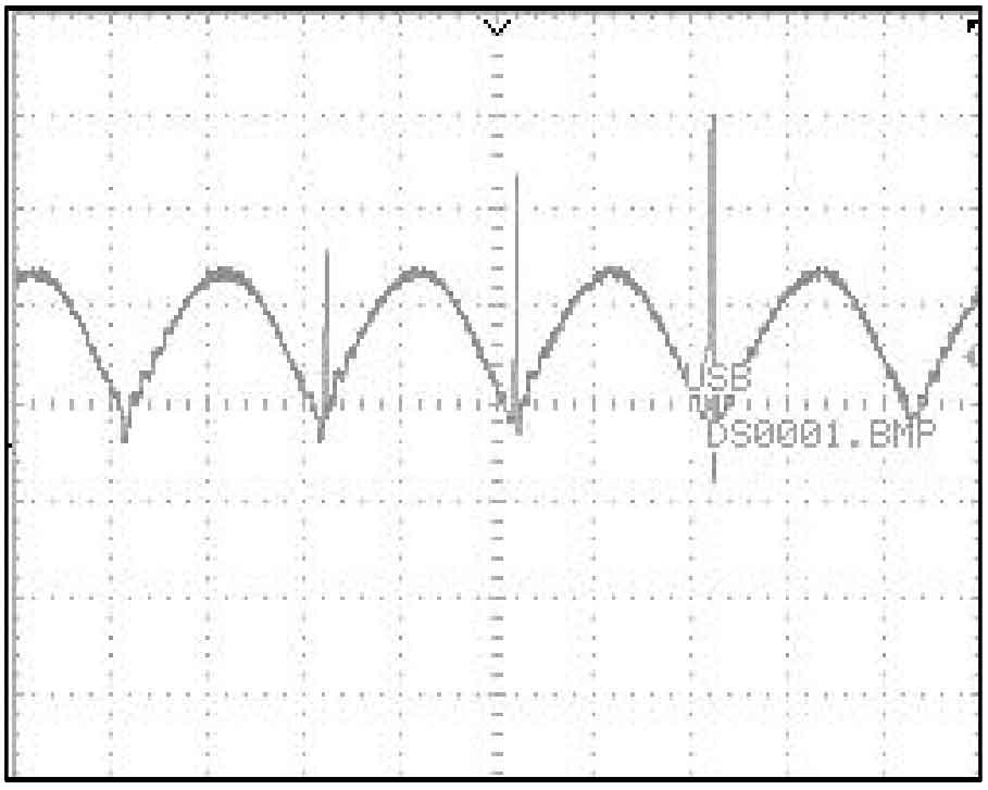
On the contrary, if the primary end has a large amount of energy, due to the limited ability of energy transmission, the amount of energy that cannot be transmitted will also increase. Even if the energy transmitted to the secondary end is sufficient to complete normal half wave waveform output, the utilization rate of its useful energy will be greatly reduced. While some related circuit components that require input power may not work properly, they may also produce incorrect output signals, The energy that interferes with the judgment of the main controller and fails to be transmitted to the secondary output end is called leakage inductance energy. Leakage inductance energy can only wait until the next switching cycle arrives, when the high-frequency power switch is turned off, and the input energy from the primary end of the transformer is transmitted to the secondary end through the flyback transformer, it is transmitted together with the energy generated in the new cycle. However, a certain amount of leakage inductance energy will be formed within each switching cycle, causing the leakage inductance energy trapped between the drain and source electrodes of the power switching transistor to continuously increase. This will result in an increasing voltage spike on the output half wave waveform, as shown in Figure 4.
If the leakage sensing energy is not processed, it will lead to useless consumption of output energy by voltage spikes, device heating, and other phenomena, resulting in a decrease in the conversion efficiency of solar inverters. In severe cases, high-frequency power switches may even be accompanied by whistling sounds, seriously threatening the normal operation of the entire machine and device safety.
To address the issue of leakage inductance energy, it is necessary to add a circuit between the power switch tube and the flyback transformer that can absorb and drain leakage inductance energy, and redirect it back to the input of the solar inverter, so that this energy can be reused in the original energy input form.
During the experiment, this article found through the study and research of relevant literature on leakage inductance that the discharge of parasitic capacitance Coss in power switching tubes can also cause a sudden increase in the drain source voltage of power switching tubes, resulting in energy loss. When designing an energy absorption circuit, it is necessary to derive mathematical formulas and calculate circuit parameters to achieve the goal of absorbing and utilizing leakage inductance energy while suppressing energy consumption caused by parasitic capacitance discharge and voltage spikes. Based on this, this article designs a new RCD leakage inductance absorption circuit, which not only absorbs and reuses leakage inductance energy, but also absorbs and utilizes the discharge phenomenon of parasitic capacitance, further improving the efficiency of useful energy utilization.
5. MPPT control algorithm design scheme
Maximum Power Point Tracking (MPPT), also known as Maximum Power Point Tracking, is an intelligent control algorithm that adjusts the duty cycle of the power switch based on input voltage and current values, changes the load impedance of the solar inverter, and matches the peak power point. The MPPT algorithm needs to have the ability to autonomously distinguish and find the maximum output power point suitable for the current moment under the intervention of environmental factors, in order to ensure that the solar inverter can output at its maximum power throughout the entire working cycle and improve the efficiency of the solar inverter.
The MPPT algorithm widely used in the design of solar inverters currently mainly comes from the following three traditional MPPT control strategies: fixed voltage control strategy, disturbance voltage control strategy, and conductance increment control strategy. The theoretical foundations of the three control strategies are different, and each involves algorithmic complexity, difficulty in signal data acquisition, difficulty in data calculation, and complexity in circuit topology.
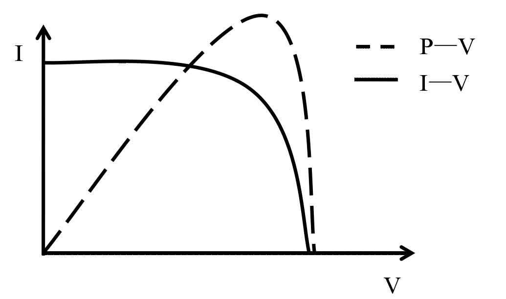
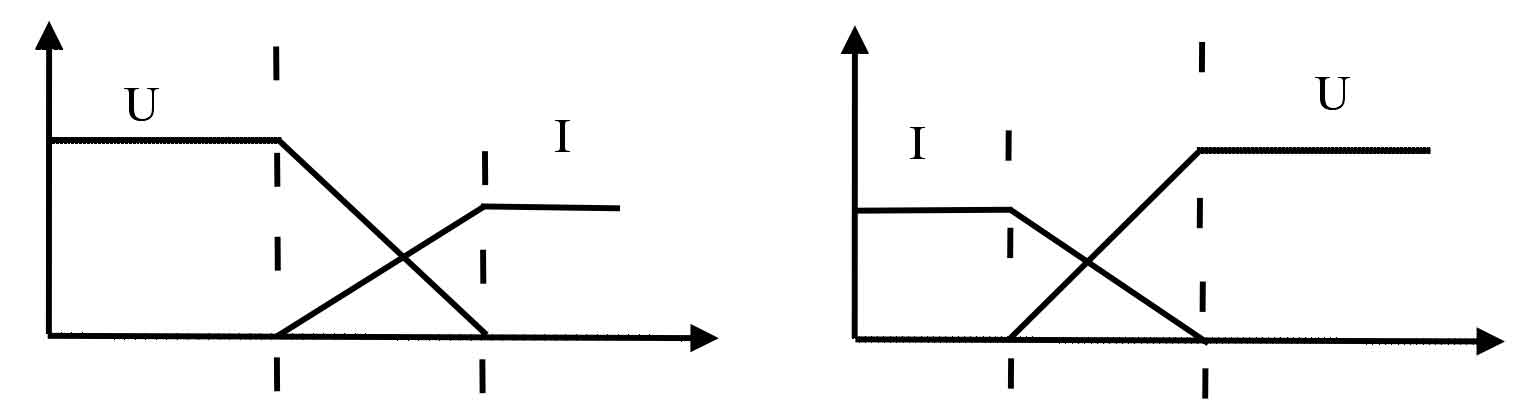
Figure 5 shows the ideal photovoltaic voltage and current relationship curve, where the vertical axis represents the DC current value at the input end of the solar inverter, and the horizontal axis represents the DC voltage value at the input end of the solar inverter. The curve relationship is abbreviated as the IV curve. The IV curve is a gradually decreasing relationship curve, indicating that the DC voltage and current converted from the photovoltaic array are limited by the power device of the solar inverter. When the power device is short circuited, the current is the maximum input value at the current moment. As the duty cycle of the voltage input controlled by the power device increases, due to insufficient voltage, the output power cannot meet the operating requirements of the device, So the current remains almost unchanged in the first half of the time, but when it reaches the conduction power threshold, the current begins to decrease and the output power continues to rise. As the input voltage continues to increase, the output power will reach its maximum value, and the solar inverter will work at the maximum power point. If the duty cycle continues to increase, the current maximum power cannot maintain the output status of the required power, and the IV curve will rapidly decrease until the input voltage reaches its maximum value when the power device is open circuit. The photovoltaic PV curve, as shown by the dashed line in Figure 5, is a unimodal curve. Due to the influence of external factors and photovoltaic materials on the photovoltaic array, the DC input of the solar inverter is different at each moment. That is to say, the photovoltaic IV curve is a dynamic relationship input curve with a constant and constantly changing voltage and current relationship. Therefore, the photovoltaic PV curve is also a dynamic relationship curve. Therefore, the maximum power point is not a fixed value, but a set of unrelated optimal solutions. The function of the MPPT algorithm is to search for the optimal solution belonging to the current time based on the IV curve that changes at that time, and stabilize the output power at that optimal solution.
Through the process of drawing the implementation concept of the traditional MPPT algorithm, it can be seen that the traditional MPPT algorithm actively applies disturbances, calculates the power value after applying the disturbance at the current moment, and compares it with the power value at the previous moment of the disturbance. This control strategy has certain high-performance requirements for circuit response speed, making it difficult to achieve real-time collection of information data. Data without real-time performance will also be unfavorable for subsequent inverter processing.
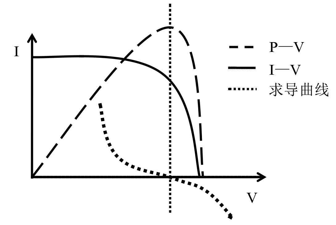
For the single peak optimal solution problem, according to the mathematical differentiation rule, it is known that if the derivative of the PV curve is taken, there is a unique zero point. For the photovoltaic PV curve, the derivative of power over voltage is taken. When the derivative value is greater than zero, it is in the monotonic rising stage, and the input voltage needs to be increased. When it is less than zero, it is in the monotonic decreasing stage, and the input voltage needs to be adjusted to decrease. When it is equal to zero, it is the maximum power point. The PV relationship curve after taking the derivative of PV is shown by the dashed line in Figure 6.
The improved algorithm still relies on real-time acquisition of the input current of the solar inverter. Although the derivative method is more convenient for single peak evaluation problems, the solution of the derivative needs to be completed through hardware circuits and hardware components. For the real-time changing photovoltaic IV curve, this algorithm poses great challenges to hardware circuit performance and processor computing speed, even in the past, it was harsh. The purpose of the MPPT control algorithm designed in this paper is to reduce the computational process while only collecting real-time input voltage data information to obtain the derivative value, and effectively control and adjust the duty cycle of the power switch to achieve maximum power point matching. It is also the current research focus and direction of the MPPT control algorithm in the field of grid connected solar micro inverter design.
Therefore, in response to the shortcomings of traditional control strategies and combining their respective advantages, this paper proposes a new type of MPPT algorithm control strategy. Without increasing the circuit topology and imposing human interference on the solar inverter during operation, the shortcomings of traditional MPPT control strategy are modified to achieve fast and efficient matching and stable output.
6. Design scheme for peak voltage suppression
In the design of solar inverters with high-frequency power switching tubes, the phenomenon of peak voltage is inevitable, and therefore, the suppression design of peak voltage is also necessary as a measure to protect the normal operation of the system and optimize system performance.
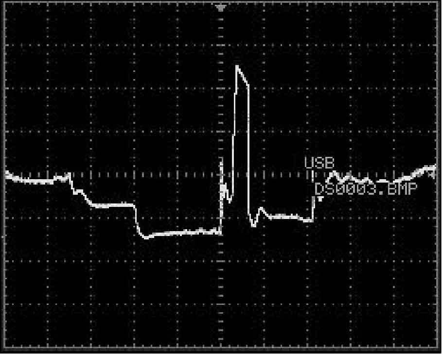
During the experiment, it was found that the voltage spike phenomenon shown in Figure 7 is commonly present in the operation of the original solar inverter. There are many reasons for the generation of peak voltage, and they all have certain correlations. For example, during the operation of the switching tube, parasitic capacitance discharge can cause the discharge voltage to be added to the drain source terminals of the switching tube, resulting in voltage peak output. The working process of the switching tube is directly related to the quality of soft switching technology implementation. The continuous accumulation of leakage energy can also lead to the generation of peak voltage, affecting the waveform output quality of the inverter half wave. A good half wave output is a prerequisite for implementing the MPPT control strategy. In addition, due to the existence of dead time in the full wave inverter section, the zero point drop phenomenon that occurs during the full wave zero crossing can also form voltage spikes in severe cases.
Based on this, when designing the complete machine of grid connected solar micro inverters, the traditional soft switching technology is first implemented to meet the power switching requirements. During normal operation, the energy loss problem caused by hard switching loss is eliminated. On this basis, targeted modifications and optimizations are made to the leakage inductance energy consumption problem in the DC-DC link and maximum power point tracking part to absorb the current spikes caused by parasitic capacitor discharge, And feedback excess leakage energy. Based on the circuit parameters introduced in the correction of leakage inductance and energy consumption issues, the soft switching technology is redesigned to make the soft switching phenomenon more obvious, reduce the possibility of peak voltage generation, and solve energy loss and peak voltage problems. Secondly, based on the resonance relationship between the parasitic capacitance, parasitic inductance, and newly introduced circuit parameters of the flyback transformer, a PI algorithm is designed to suppress the peak voltage caused by resonance. Furthermore, based on a good half wave output, design an MPPT algorithm control strategy to achieve stable output of inverter power and suppress waveform distortion and peak voltage phenomena caused by unstable power points. At the same time, based on the designed MPPT algorithm and its theoretical formula derivation, extend and modify the soft switch theoretical calculation formula, simplify the calculation process, and improve calculation efficiency. Finally, modify the traditional H-bridge inverter circuit and combine it with software control to correct and avoid voltage spikes caused by zero point drop in the full wave inverter section.
By analyzing each technology that may cause peak voltage, making necessary modifications and optimizations, suppressing the peak voltage, and through the interconnection and restraint of each link, the ultimate goal is to output the inverter full wave without peak voltage.
7. Full wave inverter design scheme
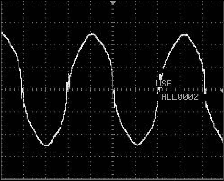
For a dual channel alternating flyback solar inverter, at the output end of the inverter half wave, the upper and lower channels each generate an inverter half wave with a period of 100Hz. During the full wave inverter process, when passing through the full bridge inverter circuit, the lower half wave is reversed by two reverse rectangular waves with a frequency of 50Hz, and then the continuous half wave is output as a 100Hz inverter full wave. This process requires aligning the zero points of two reverse 50HZ rectangular waves and two 100HZ half waves respectively, in order to ensure that the output inverter full wave is smooth and without any drop at the zero crossing point. However, if two reverse 50HZ rectangular waves are generated at the same time, when passing through the H-bridge inverter, the two signals will conflict, and the power MOSFET will be broken down, which can seriously damage the solar inverter. Therefore, in order to ensure the reliable output of the solar inverter, it is necessary to set a protection period for the reverse rectangular waves of the upper and lower circuits to prevent irreversible danger caused by the simultaneous conduction of the upper and lower circuits in the H-bridge. This protection period is called the dead time. Therefore, during the inversion of two and a half waves, there is always a time interval at the zero crossing point, and the half waves cannot be symmetrical, resulting in a zero point drop phenomenon for the entire wave at the zero crossing point. In addition, if during the process of one rectification half wave from high to zero, the half wave has not yet reached zero, while the other rectification half wave has started to rise from zero, the two half waves will overlap, and the continuous half wave after rectification will exhibit phase shift phenomenon. The adverse effect of the full wave inverter stage is shown in Figure 8. It can be seen that the output sine full wave has been severely distorted, and the breakpoint at the zero crossing point is extremely obvious. So, whether it is half wave phase shift or full wave zero point drop, it will to some extent affect the inverter efficiency and overall performance of the solar inverter.
In response to the above issues, this article introduces correction techniques for phase shift and zero point drop in the development process of the entire machine. Two power MOSFETs on the traditional H-bridge are replaced by thyristors to achieve hardware circuit zero crossing correction. Combined with external interrupt algorithms, phase shift correction is performed on the half wave output of the dual channel alternation from a software perspective, and the waveform is synchronously outputted to make the inverter waveform smooth and without any falling points.
8. Inversion efficiency
The factors that affect the inverter efficiency of solar inverters mainly include energy loss of high-frequency power switching tubes, leakage inductance energy loss, output loss caused by the output power of solar inverters not reaching the maximum power point, energy loss caused by parasitic capacitance discharge or parasitic capacitance inductance participating in resonance of circuit components, waveform loss caused by inverter waveform distortion, and peak energy loss caused by voltage spikes The energy storage consumption of large capacitors in solar inverters and the thermal energy loss caused by device heating, scalding, and even howling. It is not difficult to understand through the law of conservation of energy that the energy consumption of components necessary for the operation of the entire machine, such as the consumption of large capacitor energy storage and thermal effects in solar inverters, is inevitable. This also indicates that for a solar inverter, even if the MPPT control efficiency can reach 100%, its overall efficiency cannot reach 100%. The problem of thermal effect consumption can be solved by applying heat dissipation blocks for device protection and reducing useless thermal energy consumption. In addition, energy consumption needs to be reduced through software algorithms or hardware circuit design, continuous modification and optimization of the overall performance to continuously improve the inverter efficiency of solar energy inverters. The main task of designing solar inverters is to reduce the energy consumption of solar inverters. Through continuous optimization, the efficiency of solar inverters can be improved. Within a unit of time, more input energy can be converted into output energy, which can be integrated into the power grid to increase the power generation efficiency and total power generation of equipment. This article combines various problems encountered in the actual development process of the entire machine to develop a reasonable design scheme. The main technologies and existing problems involved above are optimized, modified, and innovatively designed to achieve the improvement of the working performance and reverse conversion efficiency of grid connected solar micro inverters.