
Although isolated solar grid connected inverters can achieve electrical isolation, it is inevitable to use isolation transformers. However, the disadvantages of isolation transformers, such as large volume, high cost, and low efficiency, cannot be ignored. In order to reduce power generation costs and improve efficiency, non isolated solar grid connected inverters can be used without the need for electrical isolation. Non isolated solar grid connected inverters can be divided into various types according to the inverter structure, The specific classification is shown in the table.
| Single level structure | Single stage non isolated photovoltaic grid connected inverter based on buck boost circuit |
| Single level structure | Single stage non isolated photovoltaic grid connected inverter based on Z-source network |
| Multi-level structure | Boost based multi-level non isolated photovoltaic grid connected inverter |
| Multi-level structure | Multi mode boost multi-level non isolated photovoltaic grid connected inverter |
Non isolated types have advantages such as small size, high efficiency, low power generation cost, and simple structure. However, due to the lack of electrical isolation and the influence of practical conditions, it is inevitable to have problems such as DC components, common mode parasitic currents, and current harmonics.
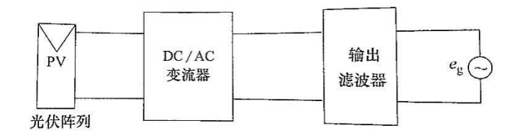
The single-stage non isolated solar grid connected inverter has only one DC/AC stage, which is relatively simple compared to the isolated structure, so the inverter efficiency is very high. Its system structure is shown in Figure 1.
In the case of low power, single-stage non isolated solar grid connected inverters usually use a buck boost circuit based solar grid connected inverter, and its circuit topology is shown in Figure 2.
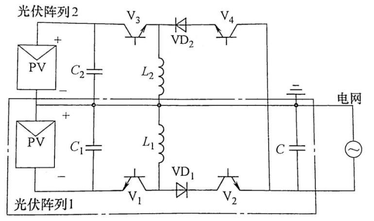
Due to the use of a buck boost circuit in its main circuit, the input voltage range is wide, and due to the energy storage effect of inductors L1 and L2, there is no need to equip a filtering inductor on the output side. The commutation process is as follows:
(1) V1 is opened, L1 is stored, and C provides energy to the grid;
(2) V2 is activated, and L1 provides energy to C and the power grid:
(3) V3 opens, L2 stores energy, and C provides energy to the grid;
(4) V4 is activated, and L2 provides energy to C and the power grid.
Two buck boost choppers work complementary at a fixed frequency, with the switch operating in a discontinuous current state (DCE) and only one set of photovoltaic arrays outputting electrical energy, resulting in relatively low efficiency.
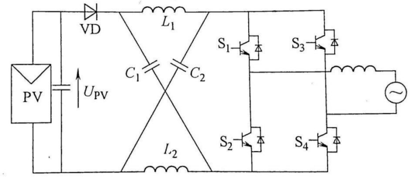
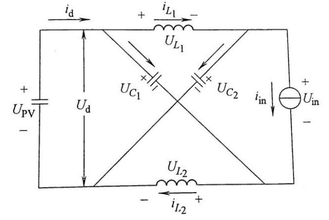
In response to the problems of adding dead time during modulation and large DC side filtering capacitor capacity in conventional single-stage non isolated solar grid connected inverters, the Z-source network non isolated solar inverter achieves the purpose of boosting voltage in a straight through state, so there is no need to add dead time. In theory, any input voltage can be connected to the grid, and its circuit topology is shown in Figure 3.
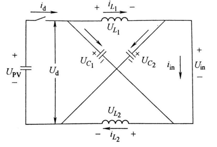
The Z-source solar inverter has two operating states within one cycle. When it operates in a non direct state, its equivalent circuit is shown in Figure 4.
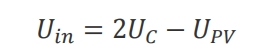
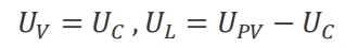
Assuming that the parameters of the Z source network are symmetric, as shown in the formula.
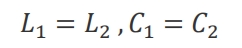
It can be inferred from the following formula.
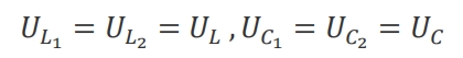
At this point, there is the following formula.
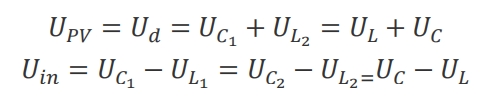
The simultaneous solution is obtained as a formula.
When the system operates in a through state, its equivalent circuit is shown in Figure 5.
At this point, due to the reverse cutoff of the diode, the following formula is shown.
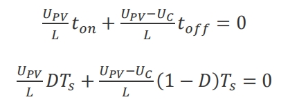
Assuming that the through state time within a switching cycle TS is T0 and the non through state time is T1, the following formula is given.
It can be seen from the following formula.
The bus voltage is shown in the following formula.
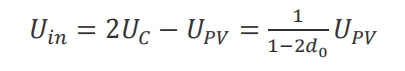
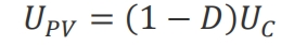
Therefore, it can be inferred that the theoretical input voltage of the Z-source solar inverter can be any value.
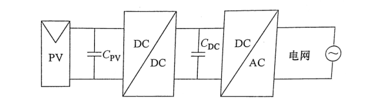
For single-stage solar grid connected inverters, both maximum power point tracking of photovoltaic modules and grid connected inverter tracking are required, and the control system is complex. Therefore, the advantages of multi-stage non isolated solar grid connected inverters are evident. The multi-stage non isolated solar grid connected inverters are mostly composed of front-end DC/DC and back-end DC/AC, and their system structure is shown in Figure 6.
The commonly used circuits for the front-end DC/DC of multi-stage non isolated solar inverters include buck circuits and boost circuits. The buck circuit is a step-down circuit, which requires a high DC voltage level on the photovoltaic array side. Increasing the photovoltaic array voltage requires connecting the photovoltaic cells in series, which can lead to hot spots and shadows. The main problem is that multiple peak states may occur, making the maximum power point not unique. Therefore, the front-end commonly uses boost circuits.
The boost circuit requires a low input voltage, so the combination configuration of photovoltaic arrays is more flexible and can ensure the tracking of the maximum power point. Moreover, because the boost circuit is grounded together with the DC/AC side, the driving of the switching transistor is convenient and the voltage stress it bears is smaller.
The basic boost multi-stage non isolated solar grid connected inverter uses a boost circuit in the front stage and a full bridge inverter in the back stage. The circuit topology is shown in Figure 7.
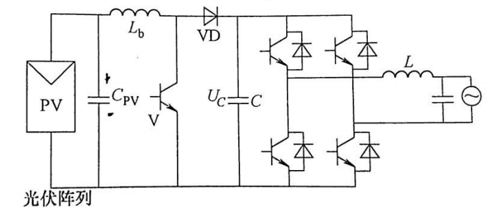
During the operation of its front-end boost circuit, when V conducts, the photovoltaic module transfers energy to LB, as shown in the following formula.
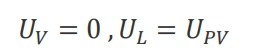
When V is turned off, the photovoltaic module and LB share the transmission capacity to C, as shown in the following formula.
When the circuit is in steady state, the current inside LB is balanced, which is the following formula.
After simplification, the following formula can be obtained.
The DC/DC conversion boost function can be achieved by changing the duty cycle D.
The latter stage full bridge inverter circuit usually uses carrier reverse unipolar frequency doubling modulation. The main principle is to use a pair of carriers with the same amplitude and opposite phase to generate a phase-shifted two-level SPWM wave after comparing with the modulation wave. Therefore, a three-level SPWM wave can be obtained on the output side of the single-phase bridge inverter circuit. The waveform is shown in Figure 8.
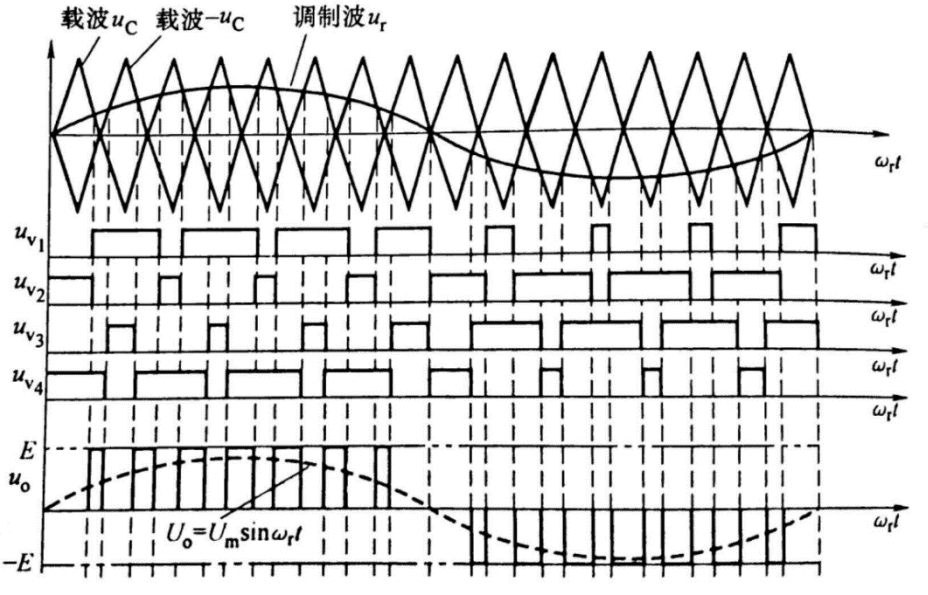
The three-level SPWM wave generated by carrier reverse modulation is twice the equivalent frequency of the two-level SPWM wave switch, which can significantly reduce the harmonic content of the output and have a significant effect on reducing the filtering inductance on the output side.
From Figure 6 and the above formula, it can be seen that the switching frequencies of the front-end DC/DC and back-end DC/AC of the basic boost multi-stage non isolated solar grid connected inverter are both high frequencies. Therefore, the issues of switching voltage stress and switching losses cannot be ignored. To compensate for the above shortcomings, a dual mode boost multi-stage non isolated solar grid connected inverter has been developed, with the main difference being the addition of two bypass diodes on the LB side. The circuit topology is shown in Figure 9.
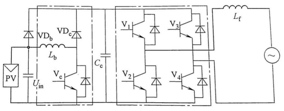
The main working principle of a dual-mode boost multi-stage non isolated solar inverter is to distinguish whether the front-end boost circuit works and the modulation mode of the back-end full bridge inverter circuit based on the absolute value relationship between Uin and Uout, so that only one set of circuits works under high-frequency switching conditions. The control principle is shown in Figure 10.
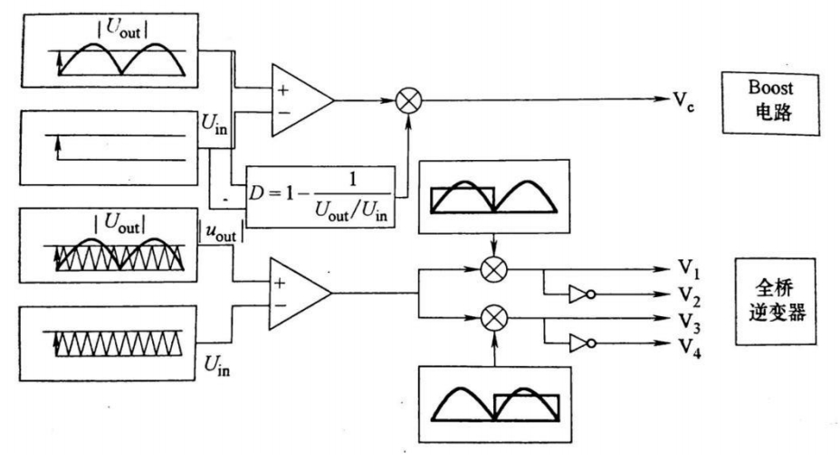
When Uin is lower than Uout, the front-end boost circuit operates, boosting the voltage to the required voltage for the back-end DC/AC, which operates in power frequency modulation mode; When Uin is higher than Uout, the front-end boost circuit continuously turns off the light tube, and the current flows from the bypass diode to the input of the back-end DC/AC. At this time, the back-end DC/AC operates in SPWM modulation mode.
Therefore, it can be seen that dual mode boost multi-stage non isolated solar inverters can not only reduce switching losses, but also greatly reduce the capacity of CC and further reduce power generation costs because the intermediate DC transition voltage does not need to be kept constant.