
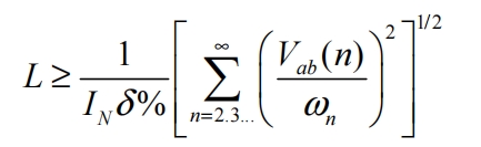
1. Filter circuit design
At present, pulse width modulation (PWM) is widely used in solar inverter technology, and the use of PWM control method will bring many high-order harmonic components to the output voltage of solar inverters, which seriously affects the voltage output quality of solar inverters. In order to obtain a purer sine wave in the output waveform of solar inverters, the selection of filters is particularly important. Filters are divided into LC, LCL, etc. for different usage scenarios. In this experimental platform, LC low-pass filters are used, and through theoretical calculations, LC filters are selected and designed.
According to the experimental platform using a solar inverter form, only the LC filter design of the three-phase solar inverter is considered in the design. For three-phase voltage type solar inverters, when using Space Vector PWM (SVPWM) control method, ignoring the losses of the solar inverter itself, the upper limit value of inductance L satisfies:

In the formula, Em represents the peak electromotive force of the power grid; Vdc is the DC side voltage value (the minimum value of the constant MPPT voltage range); Im is the peak value of the fundamental phase current on the AC side.
The formula only represents the upper limit value of the inductance under certain grid electromotive force and DC side voltage conditions, which satisfies the steady-state conditions of active or reactive power on the AC side of the voltage source solar inverter. However, considering its filtering effect, the inductance design should also meet a certain lower limit value in order to reduce high-order harmonic components and meet the standard of total harmonic distortion rate of output current. In order to calculate the lower limit value of inductance, the total distortion rate THD was determined based on actual application requirements δ % = 5% standard. Therefore, the inductance on the AC side needs to meet the following requirements:
According to the formula, the value of inductance should be greater than or equal to 0.123mH and less than or equal to 0.152mH, so an inductance of 0.15mH was selected. Based on the value of inductance, the value of capacitance can be selected, and the capacitance value is:
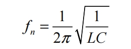
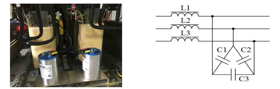
In the formula, fn is the resonant frequency of the filter, which is often taken as 0.3 times the switching frequency, i.e. 2.4kHz. The capacitance value can be calculated as 29.347uf through the formula, and the actual value is 30uf. The structure and physical diagram of the filtering circuit are shown in Figure 1.
2. Radiator selection design
In the solar inverter system, due to the highly integrated hardware and the switching frequency of the power switch IGBT reaching 8kHz, a large amount of heat is generated during the normal operation of the solar inverter, accounting for about 0.5% of the output power. If heat cannot be released in a timely manner, it will cause the temperature of the components in the system to rise, and in severe cases, it may even burn out the IGBT, affecting the normal operation of the equipment. Therefore, in the context of the continuous pursuit of solar inverter integration in the photovoltaic industry, the selection of heat sinks is particularly important.
The heat sink is installed below the IGBT, mainly for the heat dissipation of the power switch tube. Therefore, when calculating, only the heat generation of the power switch tube during operation is generally considered. For the selection and design of heat sinks, thermal resistance is the main reference for selecting heat sinks. Thermal resistance is defined as the resistance encountered by heat during the conduction process, reflecting the ability of different media to transfer heat energy. Its definition can be expressed as:
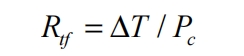
In the formula: Rtf is the thermal resistance (℃/W); Pc is the heating power (W); Δ T is the temperature rise (℃).
As it mainly focuses on the heating of power switching tubes, only the heating power of power switching tubes needs to be considered. The experimental platform used is the SKiM601TMLI12E4B IGBT from Semicon. By consulting the user manual, it was found that the maximum temperature of a single module is 125 ℃, and the heating power is:
1) At a switching frequency of 5kHz, 575W (at 55 ℃)
2) At a switching frequency of 8kHz, 756.4W (at 55 ℃)
The ambient temperature of the experimental platform is considered to be 55 ℃, and the switching frequency is 8kHz, so the heating power of the IGBT is 756.4W.
The maximum temperature of IGBT is 125 ℃, and the ambient temperature is 55 ℃. To calculate the inlet temperature of the radiator, the inlet temperature rise is:
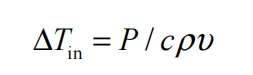
In the formula: P is the total heating power of the air flowing through the main components; C is the specific heat capacity of the air, approximately 1012J/(kg * K) (altitude 3000m); ρ For air density, approximately 0.744kg/m3 (altitude 3000m, 700Pa, 55 ℃); υ For air flow rate.
The rated heat dissipation power of the reactor is known to be about 440W, and considering the heat dissipation power of other devices, it is estimated to be about 300W. The total flow rate of the four small fans is 863.46m ^ 3/h. According to equation (4.20), the inlet air temperature rise is calculated to be 4.1k. Considering the maximum ambient temperature of 55 ℃, the maximum inlet temperature of the radiator is approximately 59.1 ℃. To increase the margin, an inlet temperature of 60 ℃ is selected. Considering that the attenuation from the junction temperature of IGBT to the shell temperature is about 15 ℃, the actual contact temperature of the radiator is about 110 ℃, and the thermal resistance value of the radiator is calculated to be 0.022 through the formula.
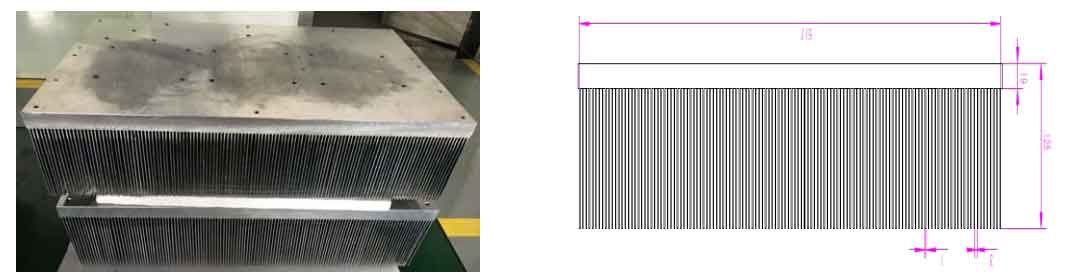
By calculating the thermal resistance value, the corresponding aluminum alloy radiator was selected. The physical and model drawings of the radiator are shown in Figure 2.
3. Stacked busbar design
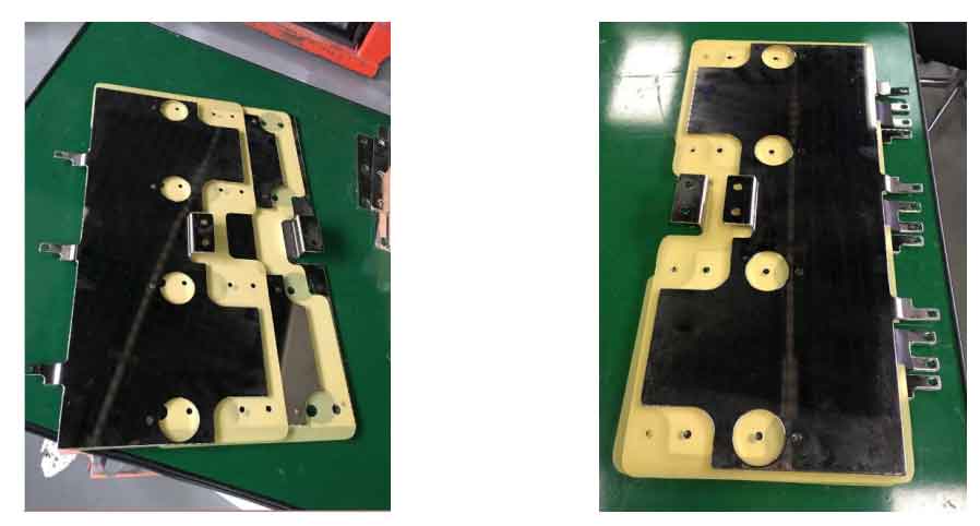
The frequency of the power switch tube used in the experimental platform reaches 8kHz, with a single switching cycle of 125us. Therefore, in an extremely short time cycle, the current flowing through the power switch tube varies greatly. If parasitic inductance is doped in the circuit, a large voltage will be generated, which will directly cause damage to the device and prevent normal and stable operation. Therefore, in order to reduce parasitic inductance, reduce the electrical distance between the IGBT and the capacitor (mainly to reduce inductive reactance), and thus reduce the high voltage generated during the IGBT switching process, it is necessary to set up specific structures between the DC bus capacitor and other devices, and the commonly used method is to set up stacked busbars. The experimental platform uses three copper bars, with insulation bars arranged between them. There are a total of five layers of busbar stacked together. This can effectively shorten the creepage distance and make the structure more compact, greatly reducing the area of parasitic inductance generation. The copper bar structure is shown in Figure 3.
4. Determination of dead time
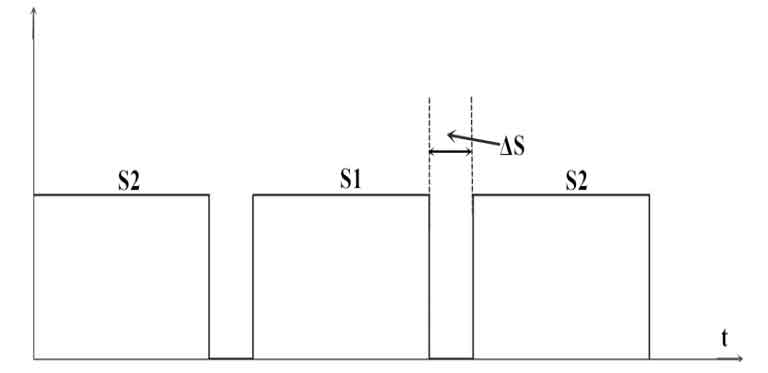
In the control process of solar inverters, due to the inherent conduction and shutdown time of power switching tubes, the conduction time of power switching tubes is often smaller than the shutdown time. The most crucial thing is that the power switching tubes on the same bridge arm cannot conduct simultaneously, otherwise it will cause a short circuit in the DC power supply and cause a malfunction. At this point, it is necessary to set a pulse blocking time for two switch tubes on the same bridge arm to ensure that the switch tubes on the same bridge arm follow the principle of “disconnect first and then open” to prevent the occurrence of through short circuits. In engineering, this blocking time is called the dead time. The power switch tube used in the experimental platform has a single switching cycle of 125us, so the dead time is set to 1us. Taking the up and down switches S1 and S2 of the same bridge arm as an example, the dead time Δ S is shown in Figure 4.
5. Experimental results
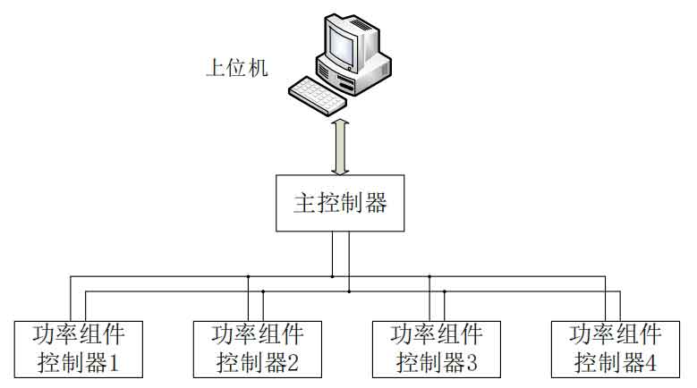
The control chip used in the experiment is a DSP produced by TI company, with the model number TMS320F28335, and an FPGA produced by Altera company, with the model number EP2C8Q208I8N. DSP is mainly used for communication between upper and lower computers, phase locking in the power grid, analog signal acquisition, and data processing. FPGA mainly connects various components of the system through 4 pairs of high-speed and low-speed optical fibers in series, achieving functions such as functional allocation, evaluation, and feedback of system faults and risks to the upper computer, and timely response. The operational flow diagram and control diagram of the photovoltaic power generation system are shown in Figures 5 and 6.
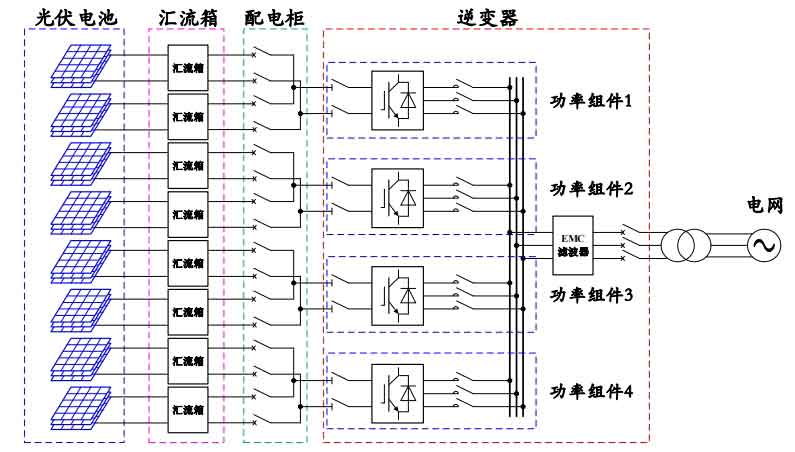
In Figure 5, the main function of the upper computer is to display the operating status and parameters of the solar inverter, and send work instructions; The main controller is mainly used for signal acquisition and processing, implementation of MPPT algorithm, coordination control system, and protection system; The power component controller is mainly used for signal acquisition and processing (voltage and current/switch quantity/temperature, etc.), control command generation (current regulation/PWM modulation/internal protection, etc.), and communication with the main controller.
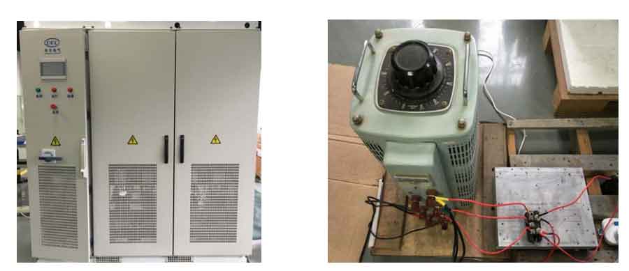
The cabinet and voltage regulator composed of various devices required for the experiment are shown in Figure 6.
The experiment uses a T-type three-level solar inverter selected from the previous text, with a switching frequency of 8kHz and SVPWM modulation method. The grid voltage is 315V, the grid frequency is 50Hz, the power factor is 0.9, and the rated output power of a single module is 125kW. Other relevant parameters are calculated based on the previous text. The waveforms of the grid voltage and DC voltage are shown in Figure 10.
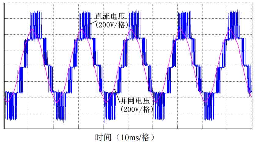
As shown in Figure 7, the DC voltage is controlled by a T-type three-level switch structure, and the waveform exhibits unique output characteristics of the three-level structure. However, there are still some burrs that require further filtering to achieve more ideal DC voltage quality.
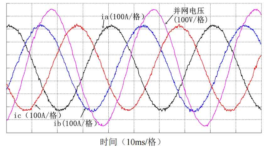
When conducting experiments on grid connected photovoltaic inverter systems, the waveforms of three-phase grid connected current and grid connected voltage are shown in Figure 8.
Figure 8 shows the three-phase grid connected current of the solar inverter at full load of 125kW, with a phase difference of 120 ° for each phase, and an effective value of 230A; The effective value of grid connected voltage is 315V.
6. Summary
According to the requirements of conducting experiments on photovoltaic inverter systems, important hardware and parameters within the system were selected and calculated. Considering some possible issues in the entire inverter system, such as load imbalance, high temperature of power switching tubes, detailed calculations and selections were made for DC bus capacitors, filtering circuits, stacked busbars, and dead time, and corresponding devices that meet the system’s requirements were found. Through the grid connected power generation experiment of the inverter system, the rationality of device selection has been verified, and it is also a affirmation of the structure selection and MPPT algorithm optimization of the solar inverter, achieving the goal of improving the efficiency of the solar inverter.