
Based on the three-level adjustable two-stage solar inverter and its control strategy proposed in this article, to verify its feasibility, a simulation platform was built using MATLAB/Simulink and verified through simulation.
This simulation system separately modulates the front-end voltage regulation circuit and the back-end inverter circuit. The front-end voltage regulation circuit modulates the dual power supply system into bus and midpoint voltages that vary regularly. After being output by the back-end solar inverter, it undergoes LC filtering and is delivered to the star connected three-phase load. The system sampling time is set to 0.2 us, and the simulation time is set to 0.06 s. The main simulation parameters are shown in Table 1:
| Type | Parameter |
| fs | 15kHz |
| E1、E2 | 400V |
| Um | 311V |
| fc | 50Hz |
| Lr1、Lr2 | 27uH |
| L1、L2 | 680uH |
| L3、L4 | 1.02mH |
| C3、C4 | 6.2uF |
| La、Lb、Lc | 3.1mH |
| Ca、Cb、Cc | 2uF |
| Ra、Rb、Rc | 5Ω |
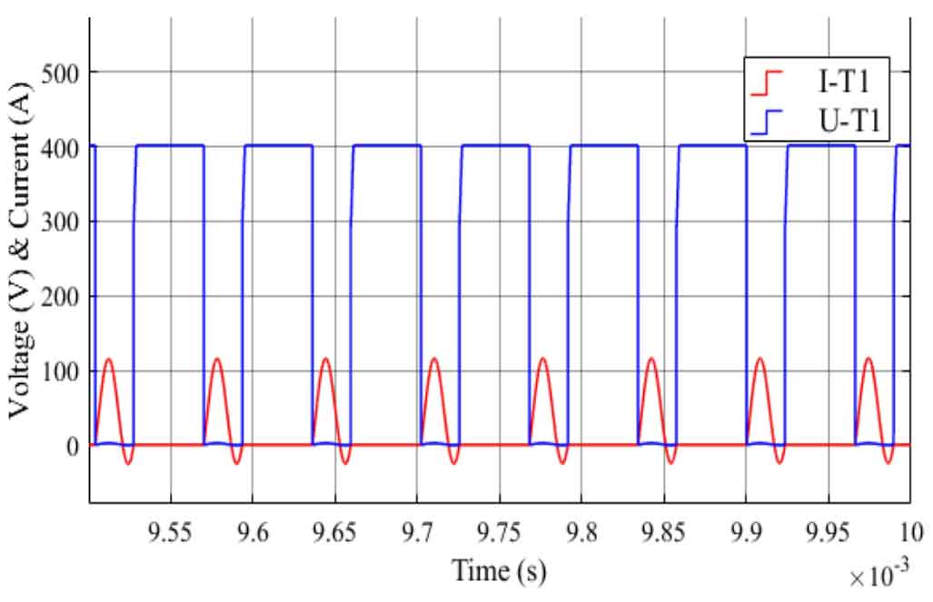
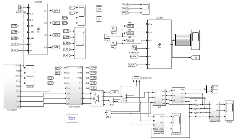
Figure 2 shows the voltage and current waveform of T1 during a certain window time. When the switching transistor T1 is turned on, the current slowly rises from 0 and after passing through resonance mode, it turns off at 0, achieving zero current on and off. During the switching process, the product of voltage and current is close to 0, indicating that the new soft switch introduced in the front-end circuit in this article is feasible and helps to further improve the inverter efficiency.
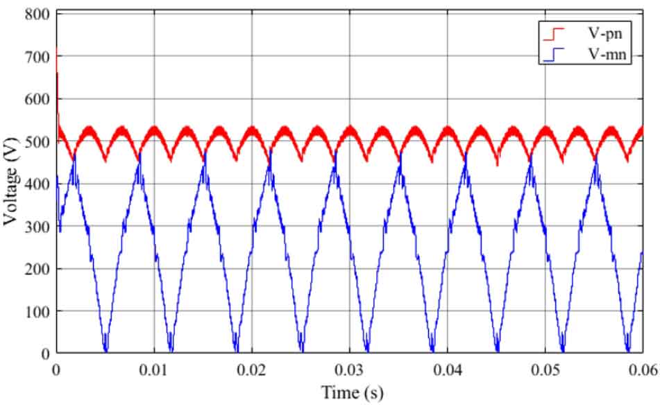
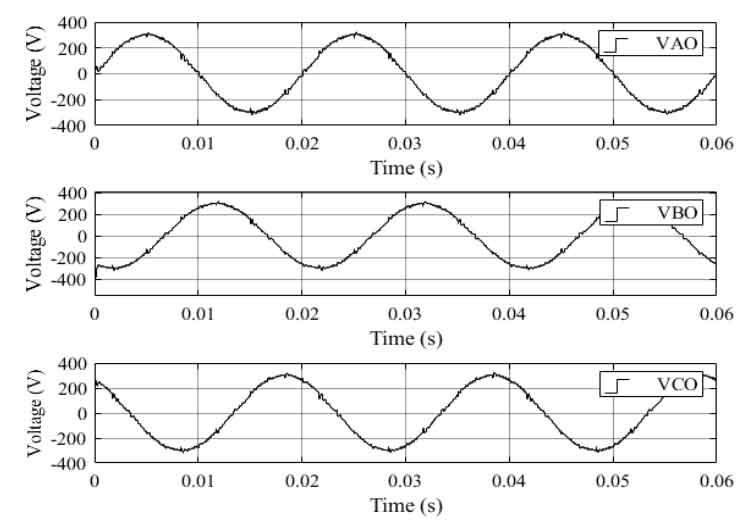
The voltage of the busbar and midpoint varies according to the set waveform. The distortion rate of the busbar voltage is low, but there are certain voltage ripples, mainly caused by the small equivalent capacitance. The problem of significant voltage waveform distortion in the midpoint voltage is mainly due to the use of hard switching in T3 and T4. Additionally, due to the voltage divider effect of output capacitors C3 and C4, the midpoint voltage is also affected by the bus voltage, but it does not affect its power output characteristics. In an ideal state, the subsequent inverter circuit only needs to switch the switch during the corresponding state transition to achieve the expected purpose. The waveform of the A-phase bridge arm switch is shown in Figure 4:
Taking phase A as an example, within a fundamental period Tc (0.02 s), for the convenience of description, the initial phase is chosen as π/6. At 0 to Tc/3, switch tubes Q1a and Q2a conduct, and at this time, phase A is always connected to the high-level line P. The bus voltage starts to decrease after passing through two peaks until it reaches the same level as the midpoint voltage. At Tc/3 to Tc/2, switch tubes Q2a and Q3a conduct, and at this time, phase A is always connected to the intermediate level line M. Afterwards, the midpoint voltage begins to decrease until it drops to 0. At Tc/2 to 5Tc/6, switch tubes Q3a and Q4a conduct, and at this time, phase A is always connected to the low-level line N. At 5Tc/6 to Tc, switch tubes Q2a and Q3a conduct, and phase A is connected to the intermediate level line M. The midpoint voltage starts to rise until it is equal to the bus voltage at the beginning of the next cycle, so that the voltage before and after each switch switching remains basically unchanged. From this, it can be seen that within one switching cycle, the subsequent inverter circuit only needs to change the switching state four times per phase. The time for connecting the high-level line is Tc/3, the time for connecting the low-level line is Tc/3, and the time for connecting the intermediate level line is two Tc/6.
In order to more intuitively reflect the degree of reduction in the switching frequency of the two-stage inverter structure proposed in this article, it is compared with the switching waveform of a regular three-level solar inverter.
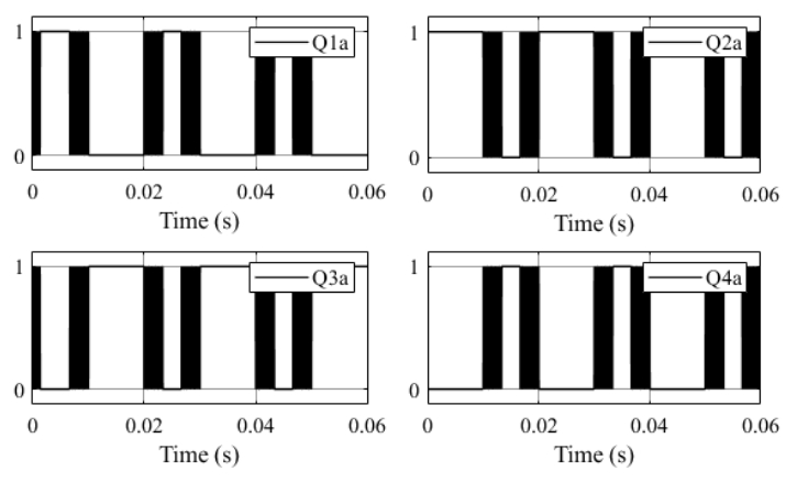
Figure 5 shows the discontinuous pulse width modulation (DPWM) used by traditional three-level solar inverters to reduce switching frequency. The principle is to inject zero sequence components into a reference sine wave, that is, select a suitable zero vector within three adjacent vector sectors, so that each group of switches can have no switching action within 120 °. In an ideal state, the switching frequency can be reduced by one-third.
The PWM modulation strategy based on line voltage proposed in this article utilizes the bus and midpoint voltage with varying output patterns of the front-end voltage regulation circuit to be used in conjunction with the back-end inverter circuit. It only needs to be turned on and off four times in one cycle. Compared with the traditional three-level solar inverter DPWM modulation, it greatly reduces the switching frequency of the back-end inverter circuit and simplifies the modulation method.
The two-stage inverter structure proposed in this article has a very obvious sinusoidal characteristic of the phase voltage waveform without filtering, and the variation per unit time is small. This indicates that the new two-stage inverter structure and its modulation method proposed in this article are feasible. The output voltage of the later stage inherits the voltage ripple of the busbar and midpoint, and its fluctuation degree is reduced due to mutual cancellation. It is quite obvious that during the commutation phase, the switching state of the later stage inverter circuit causes certain voltage ripple. When each phase voltage is at 0 V, there is also a noticeable voltage ripple, which is caused by the switching of switch tubes T3 and T4 in their critical operating time domain. These voltage ripple can be eliminated by LC filters.
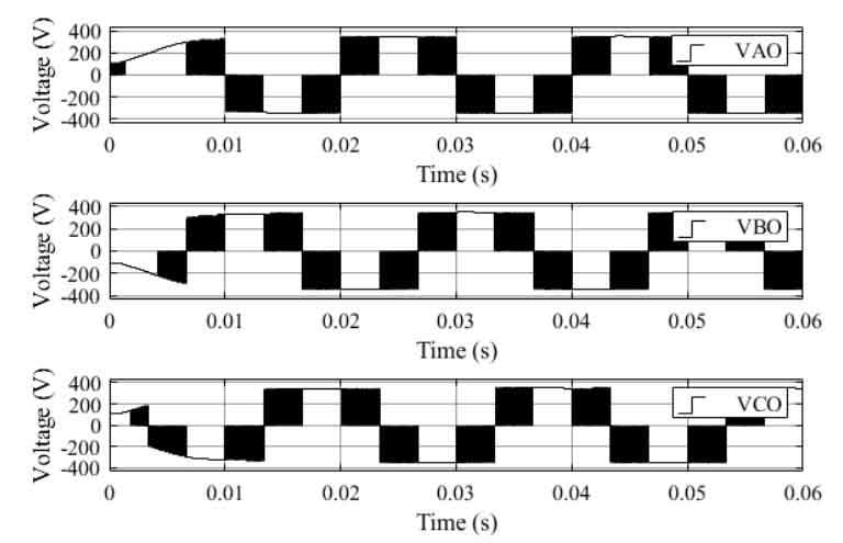
Figure 7 shows the unfiltered phase voltage waveform of a three-level solar inverter under DPWM modulation. Due to its high-frequency switching state for 2/3 of the time, the phase voltage undergoes significant high and low changes for most of the time, and the high-frequency characteristics are still quite obvious. This results in high inductance and switching losses, which limits the advantages brought by the three-level solar inverter.
Compared with traditional three-level solar inverters, the three-level adjustable solar inverter proposed in this article outputs an adjustable voltage through the front stage voltage regulation circuit, and the back stage inverter circuit does not require the turn-on transistor to be in a constant on/off state to maintain volt second balance, greatly reducing the switching frequency of the solar inverter. At the same time, the phase voltage changes less per unit time, which reduces the loss of the LC filter, This is also where the two-stage inverter scheme proposed in this article is superior to the traditional two-stage inverter scheme.
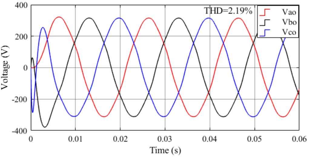
The two-stage inverter structure proposed in this article has a three-phase voltage output through an LC filter. The voltage waveform is relatively regular, and the amplitude frequency characteristics meet the set requirements. The total distortion rate (THD) is 2.19%, which is lower than the requirement of THD not exceeding 5% under normal operating conditions of the power grid.