
The system introduces the three-level adjustable two-stage solar inverter proposed in this article. The solar inverter has the following innovations: a new two-level inverter topology structure and a front and rear joint control strategy.
Efficiency is particularly important in photovoltaic power generation, as it can bring considerable economic benefits. Switching loss and inductance loss are the main losses of solar inverters. In this paper, a three-level adjustable method is adopted to make the switching loss and magnetic loss of the subsequent three-phase inverter circuit close to 0. At the same time, soft switching is added to the previous stage, greatly reducing the switching loss and magnetic loss of the previous stage circuit. These advantages make the inverter structure proposed in this paper very efficient and have the potential to become more efficient Lower cost solar photovoltaic inverter products.
This article introduces several main multi-level solar inverters currently used, among which the NPC type solar inverter is the most widely used. Due to its structural characteristics, it is easy to generate midpoint potential drift, which increases modulation difficulty. The inverter structure proposed in this article can effectively solve this problem.
1. New two-stage inverter topology structure
Due to the significant influence of temperature and light intensity on the photovoltaic array, it causes a change in the maximum power point and affects the DC input voltage. When the maximum power point of the photovoltaic array changes and the output voltage is low, high-power photovoltaic power stations mainly adopt single-stage inverter structures that output low voltage and high current, which greatly increases costs and conduction losses. When the online voltage is 380 V and connected to the grid, a two-stage inverter scheme is usually used. The front stage adopts a boost structure to obtain a stable voltage for the later stage inverter. This structure greatly increases its switching and conduction losses, and also poses challenges to the cooling design and service life of components. Moreover, the existing three-level inverter schemes always require regulating the intermediate potential balance, which limits the superiority of three-level solar inverters. This not only increases the modulation difficulty, but also fails to fully utilize the relationship between the front and rear stages.
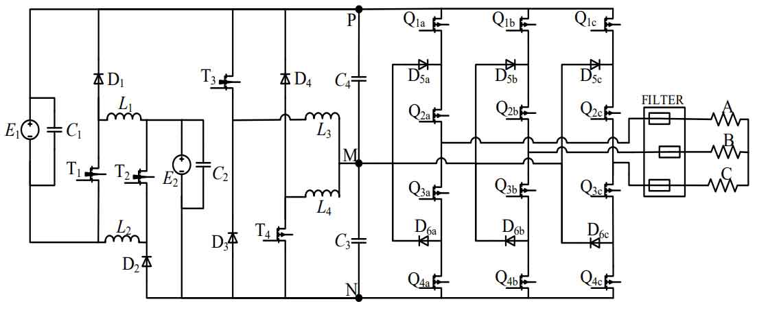
To solve the above problems and fully leverage the advantages of three-level solar inverters, this paper proposes a three-level adjustable two-stage solar inverter. The inverter system includes a front-end voltage regulation circuit, a back-end inverter circuit, and a three-phase LC filter, with the three-phase load connected in a Y-shape. Record high potential as point P, middle potential as point M, and low potential as point N. The front-end voltage regulation circuit can effectively reduce the switching frequency and voltage before and after the switching of the back-end inverter by adjusting the bus voltage (VPN) and midpoint voltage (VMN), and also reduce leakage current, thereby greatly improving work efficiency.
The front-end voltage regulation circuit is powered by two overlapping DC power sources E1 and E2. In an ideal state, E1=E2, and L1 and L2 form an inductive charging path when T1 and T2 are closed, respectively. When T1 is disconnected, inductance L1 and freewheeling diode D1 form the first discharge path. When T2 is disconnected, inductor L2 and freewheeling diode D2 form a second discharge path, and the bus voltage VPN can be adjusted by controlling the duty cycle of switches T1 and T2. The two charging and discharging paths have symmetry and complementary operation, with the aim of balancing the discharge of the two DC power sources.
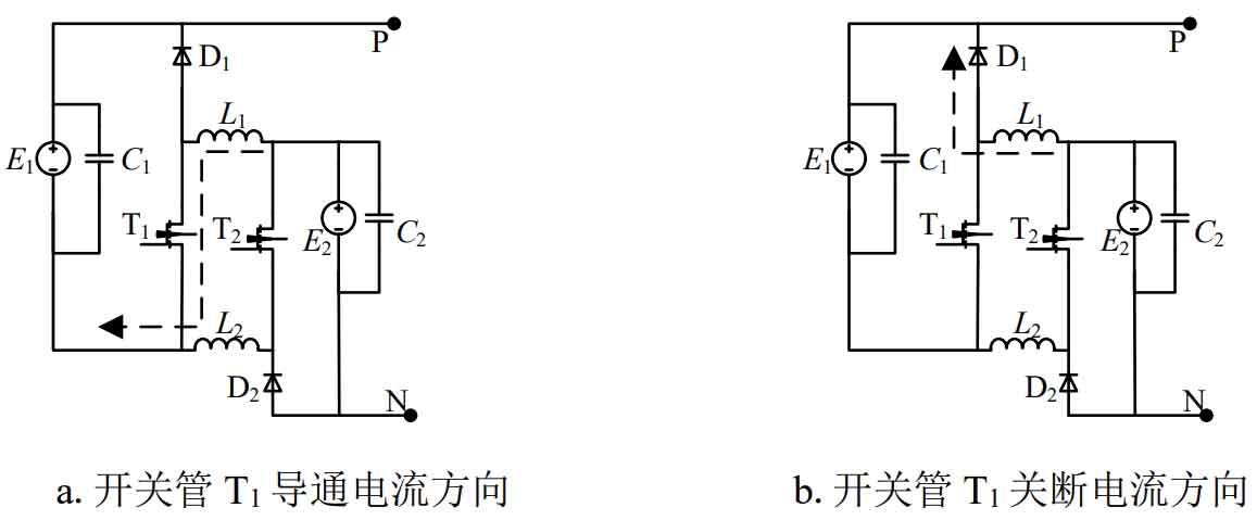
Figure 2 (a) shows the current direction of inductor L1 when switch tube T1 is conducting. When switch tube T1 is conducting, the current flows from the positive pole of power supply E2 through inductor L1 and switch tube T1 to the negative pole of power supply E1. Finally, the energy of the two DC power sources is released on the bus, and the inductor is in a charging state. Figure 2 (b) shows the current directions of the two inductors after the switch tube T1 is disconnected, and inductor L1 continues to release current to the high-level line P through the freewheeling diode D1.
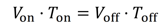
If the duty cycle of the switch is recorded as DT, then DT=Ton/TS, where Ton is the conduction time of the switch within one switching cycle, and TS is one switching cycle. According to the principle of voltage second balance between charge and discharge of inductors, that is, the surface product of the voltage second curve during the conduction and turn off time periods of inductors in charge and discharge balance is equal. The relationship between the duty cycle of T1 and the bus voltage can be derived.
There is a voltage second balance relationship, where Von is the voltage at both ends of the inductor when the switch conducts within one cycle, Voff is the voltage at both ends of the inductor when the switch turns off within one cycle, and Toff is the time of disconnection:
When T1 is working, its volt second balance relationship can be written:
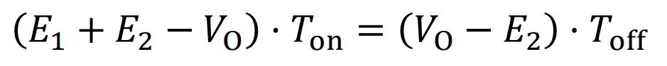
Assuming that the voltage of two DC sources is equal to E, and the output voltage VO is the bus voltage VPN, the relationship between the bus voltage and the duty cycle DT1 of T1 switch can be obtained:
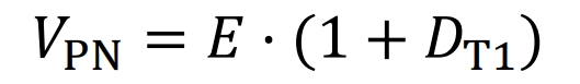
From the formula, it can be concluded that VPN and DT1 are linearly positively correlated. When the switch duty cycle DT1 is 0, the bus voltage is a single DC power supply voltage E. When the switch duty cycle DT1 is 1, the bus voltage is equal to the sum of the two DC power supply voltages 2E. By controlling the duty cycle of T1 switch, the bus voltage can be effectively adjusted, with a range of E-2E. The effect of switching tube T2 on regulating the busbar is the same as the above process. T1 and T2 work complementary to each other, ensuring that the discharge of two DC power sources is balanced. In the calculation process, it can be equivalent to continuous operation of one switching tube.
The front-end voltage regulation circuit also includes a forward buck converter composed of switching transistor T3, freewheeling diode D3, inductor L3, capacitor C3, and DC bus PN; And a negative buck converter composed of switching transistor T4, freewheeling diode D4, inductor L4, capacitor C4, and DC bus PN. The voltage at points P and M is VPM, while the voltage at points M and N is VMN. Due to the use of small capacity capacitors for C3 and C4 to achieve rapid adjustment of the midpoint voltage, the amount of charge stored by the two capacitors is very small. Therefore, the current generated by the charging and discharging of the busbar can be ignored, and only the ability of midpoint M to obtain push-pull current from inductors L3 and L4 is considered.
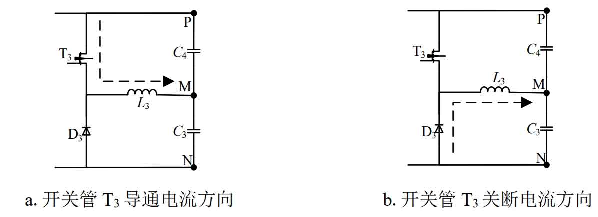
Figure 3 shows the schematic diagram of the forward buck converter, with the DC bus P as the input terminal, N as the common terminal, and the midpoint M as the output terminal. When switch tube T3 is conductive, the bus charges inductor L3, and the current passes through inductor L3 to midpoint M. When switch tube T3 is disconnected, inductor L3 discharges capacitor C3 under the action of freewheeling diode D3, forming a forward buck converter. At this time, midpoint M has the ability to output current. According to the principle of volt second balance, the relationship between midpoint voltage VMN and bus voltage VPN can be derived:
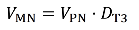
Among them, DT3 is the duty cycle of switch tube T3. According to the formula, the voltage VMN at point M increases linearly with the duty cycle of switch tube T3. When a load is connected between midpoint M and common terminal N, the voltage at point M can be adjusted arbitrarily by adjusting the duty cycle of switch tube T3, with an adjustable range of (0 to VPN). The reason for using a forward buck converter here is that during the working cycle of T3, the intermediate level at point M needs to output current.
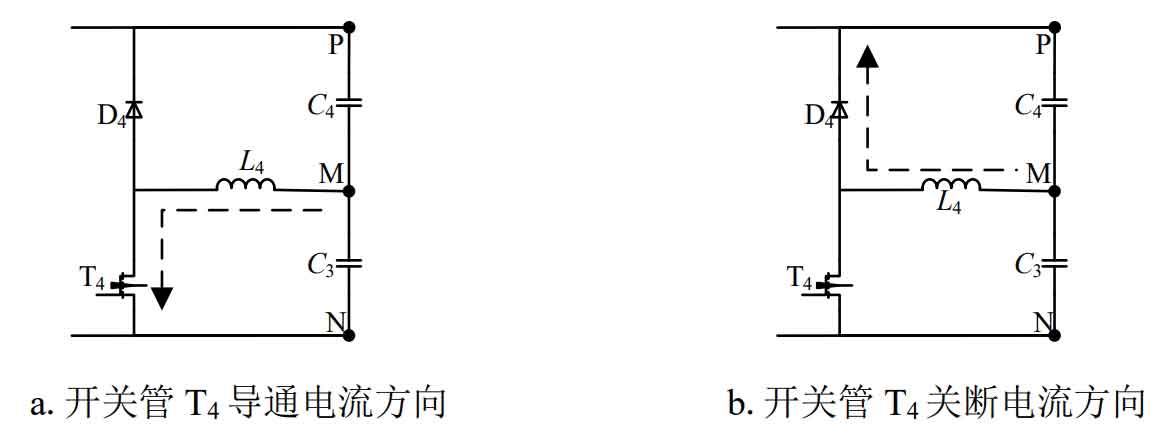
Figure 4 is a schematic diagram of the negative buck converter, with the low-level line N as the input, the high-level line P as the common terminal, and the intermediate level line M as the output terminal. When the switch tube T4 conducts, the bus charges the inductor L4, and the current flows through the midpoint M to the inductor L4. When switch tube T4 is disconnected, inductor L4 starts discharging capacitor C4 under the action of freewheeling diode D4. According to the principle of volt second balance, the relationship between VPM and bus voltage VPN can be deduced:
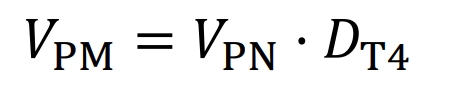
Among them, DT4 is the duty cycle of the switch tube T4, which can be obtained from equation (3.5). VPM is directly proportional to the duty cycle DT4 of the switch tube T4. When connecting loads between P and M, VPM can be adjusted arbitrarily by adjusting DT4, with an adjustable range of (0 to VPN). Due to the relationship between VPN=VPM+VMN at points P, M, and N, the relationship between the midpoint voltage VMN and the variation of bus voltage during the operation of switch T4 can be written as follows:
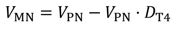
The formula shows a negative correlation between the midpoint voltage VMN and the duty cycle of switch T4. By controlling the size of DT4, the midpoint voltage can be effectively adjusted. A negative buck converter is used here, as the intermediate level M point needs to have the ability to absorb current during the operation of switch T4.
The above is the principle of adjusting the bus and midpoint voltage through corresponding switch tubes, and the working process of the subsequent inverter circuit can be roughly described as follows:
The three-phase symmetrical load is connected in a Y-shape, and the phase with the highest phase voltage in the time domain is referred to as the H-phase; The phase with the lowest phase voltage is the L phase; The phase voltage at the intermediate level is referred to as M phase. If there is a switching trend between phase H and phase M in the solar inverter at a certain moment, switch tube T3 will act, causing the midpoint voltage VMN to increase, while switch tube T1 will act, causing the bus voltage VPN to decrease, to ensure that the voltage change of the switch tube during the commutation process of phase H and phase M is relatively small.
If there is a switching trend between phase M and phase L in the solar inverter, the switch tube T4 will act, causing the midpoint voltage VMN to decrease, i.e. VPM to increase. At the same time, the switch tube T1 will act, causing the bus voltage VPN to decrease, in order to ensure that the voltage change of the switch tube during the commutation process of phase L and phase M is relatively small.
If the voltage at both ends of each inductor of the filter is adjusted to a very small value, which is exactly equivalent to changing the voltage difference of each phase switch, there is no need to perform switch action to maintain volt second balance, so that the switching transistor in the inverter circuit does not operate within a certain range. Within this range, the H-phase is always connected to the high-level line P, the M-phase is always connected to the intermediate level line M, and the L-phase is always connected to the low-level line N.
2. Front stage circuit soft switch design
From the previous work process, it can be seen that the current of the busbar and intermediate level line both come from the charging and discharging paths of the two DC power sources. Therefore, the switching transistor T1 has a relatively large current in its working state, and its switching quality greatly affects the quality of the output voltage waveform and conversion efficiency. In the field of power electronics, it can be divided into hard switches and soft switches according to their switching characteristics.
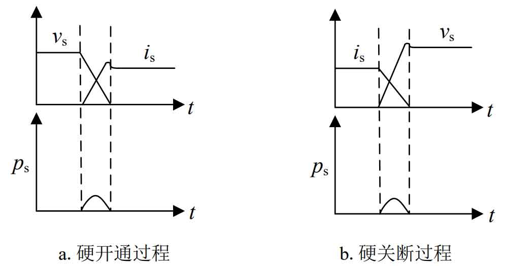
Vs represents the voltage at both ends of the switch; Is represents the current passing through the switch; PS represents switch loss. Hard switching belongs to the forced switching process, which conducts when the voltage is not zero and turns off when the current is not zero, resulting in a significant intersection between the voltage and current during the switching process, forming switching losses and generating switching noise. If T1 adopts a traditional hard switch, it will cause significant noise during the turning on and turning off moments, seriously affecting the waveform quality of the output voltage of the front stage, and thus affecting the output voltage quality of the rear stage inverter circuit. Moreover, during the switching process, the product of voltage and current is large, which will result in significant losses for the switching transistor T1. Compared with the single-stage inverter scheme, it has no obvious advantage in efficiency and is prone to overheating.
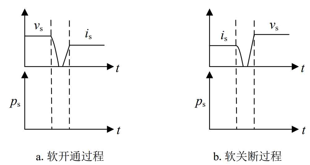
The design method of soft switching is to add capacitors and inductors to the original circuit, taking advantage of the characteristic that the voltage phase of the capacitor will lead the current of the inductor during LC resonance, so that the switch will turn off when the current naturally crosses zero, and the device will conduct when the switch current crosses zero, thereby achieving the goal of reducing switch noise and losses.
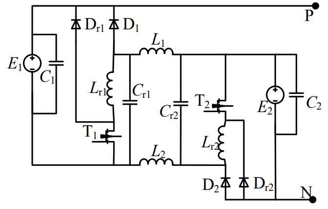
In order to further improve the conversion efficiency and power density, an inductor Lr1, a capacitor Cr1, and a diode Dr1 are added to the original circuit to form a zero current switching resonant circuit, enabling it to switch in a zero current state. T1 can be divided into four working modes within a complete switching cycle:
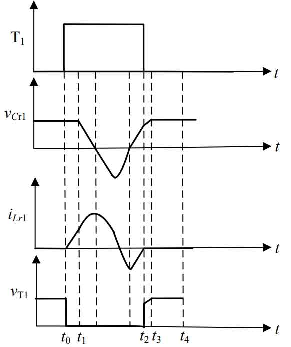
During the time period from t0 to t1, switch T1 conducts at t0, and the current of inductor Lr1 increases linearly. At t1, the current rises to be equal to the output current, and this time period ends.
During the time period from t1 to t2, capacitor Cr1 and inductor Lr1 are in a full wave resonance state, and the electric and magnetic field energy are converted to each other until the switch is disconnected at t2.
During the time period from t2 to t3, in capacitor charging mode, inductor L1 charges Cr1 until the voltage of Cr1 is equal to the voltage of a single DC power supply at time t3.
During the time period from t3 to t4, in turn off mode, inductor L1 continues to flow to the bus through diode D1 until entering the next switching cycle, achieving zero current switching throughout the entire switching process.