
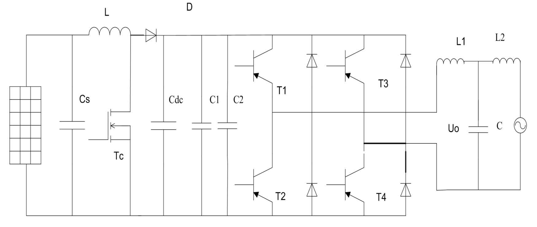
1. System structure and design requirements
The main circuit diagram structure of the system has been shown in the diagram. For the parameters in the circuit, a 5kW household solar photovoltaic grid connected power generation system should have the following requirements:
1) Solar cell input voltage range: Vpv=200V-600V
2) Solar cell input power: Ppv=5000W
3) Rated power of solar inverter: 5kW,
4) Solar inverter output voltage: 220V ± 5%
5) Output frequency: 50Hz ± 4%
6) DC/DC switching frequency: 40kHz, DC/AC switching frequency: 5kHz
7) Insulation method between solar inverters and public power grids: no transformer
The above are the approximate parameters of the system. Next, we will discuss the specific parameters in each module of the system.
2. Selection and layout of solar cells
As can be seen from the previous chapters, there are currently three commonly used types of solar cells: monocrystalline silicon, polycrystalline silicon, and amorphous silicon. Among these three categories, the utilization rate of monocrystalline silicon solar photovoltaic cells is around 15% -20%, with a service life between 15-20 years. The solar photovoltaic utilization efficiency of polycrystalline silicon and amorphous silicon cells is around 10%, so based on this, we choose monocrystalline silicon photovoltaic cells with better performance.
Due to the parameter that the power of the photovoltaic panel is 5kW, it is possible to choose to use a photovoltaic battery pack with a total power of 5kW. Therefore, among the comparison and selection of various types of monocrystalline silicon solar cells, this project selects the XH-L100M monocrystalline silicon solar cell model, where the maximum output power of a single cell is Pm=100W, and the total battery module is composed in series, so a total of 5000W/100W=50 is required. A total of 50 pieces, considering the margin issue, it is best to use 55 pieces in practice. The specific parameters of this model are as follows:
1) Open circuit voltage Uoc=21.5V, maximum power point output voltage Um=16.5V
2) Short circuit current Isc=6.8A, maximum power point output current Im=6.2A
3) The lifespan of photovoltaic cells is greater than or equal to 20 years
4) Photovoltaic conversion efficiency; 16%
In terms of solar cell array layout and installation, the installation angle of the solar cell array is first calculated based on the height angle of the sun at 12:00 noon when the light is strongest:
Taking the Wuhan region as an example, Wuhan is located at 113.41 ° -115.05 ° E and 29.58 ° -31.22 ° N, and the direct solar angle H=26.26 ° can be obtained from the formula of the direct solar angle, where α To calculate the geographic dimensions of points, β The geographical dimension of the point of direct sunlight is 23.26 °.

According to the formula, the installation angle Q of the solar cell array can be calculated as 63.34 °.
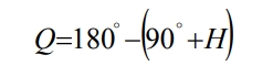
In order to facilitate the installation of solar panels, the inclination angle should be rounded and the final installation angle should be 65 °.
3. Main parameter design of Boost circuit
The output voltage of the photovoltaic panel is between 200-600V, and the DC/DC conversion circuit uses a Boost circuit. Below are the parameter settings and device selection for the key components in the Boost circuit.
3.1 Boost circuit boost inductance setting
The duty cycle formula for the Boost converter circuit is:
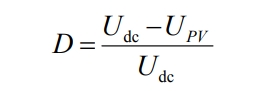
From the formula, it can be seen that when the input voltage Upv decreases, in order to ensure that the output voltage Udc does not change too much, it can be maintained stable by increasing the duty cycle. However, due to the inherent resistance (parasitic resistance) of the converter in practice, this limits the range of duty cycle adjustment. When the adjusted duty cycle exceeds the range, the output voltage Udc will not only not remain stable, but may even decrease. To prevent this phenomenon from occurring, the control of the duty cycle in practice must be within 0.88. And in the design of inductors, ripple (AC component caused by DC voltage fluctuations) factors should also be considered. The specific formula is as follows:
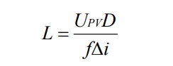
In the formula, D is the duty cycle, and combined with the previous description, its maximum value is 0.88. f is the switching frequency, with a magnitude of 40kHz, Δ I is the AC current generated by fluctuations, and Upv is the output voltage of the photovoltaic cell, ranging from 200 to 600V. When the input voltage is around 200V and the current is around 30A, the solar cell operates at its maximum power point, corresponding to a maximum duty cycle of 0.88, where Δ The coefficient of i is set to 0.25. The data is inputted into equation 3.4, resulting in L=0.58mH. So the value of the boost inductance is set to 0.58mH.
3.2 Boost circuit capacitance setting
a. Protective capacitor setting
Considering the influence of ripple current in the Boost circuit, it is necessary to install a capacitor in the circuit, so that the capacitor and the distributed inductance on the circuit form a simple filter to reduce interference in various parts of the circuit. After reading a large amount of literature and experiments, the circuit capacitance was set to C=500uF. Due to the potential voltage that the capacitor may withstand being around 600V, a 100K resistor must also be connected in parallel with the capacitor to achieve parallel voltage equalization and protect the components in the circuit.
b. Support capacitor setting
From the input and output voltage relationship of the Boost converter circuit, it can be known that Udc/Upv=1/1-D, thus obtaining Idc/Ipv=1/1-D. In addition, according to the basic capacitance calculation formula I=C (dU/dt), it can be obtained that:
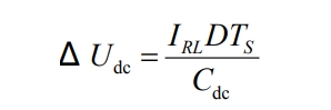
In the formula, IRL is the output current, D is the duty cycle of the Boost circuit, and TS is the switching cycle. According to the formula and the power calculation formula P=UI, multiply the left semicolon up and down by Udc to obtain:
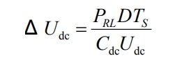
Based on the concept of ripple current mentioned earlier, it can be inferred that in the above equation Δ Udc/Udc is the ripple voltage coefficient, where the ripple voltage coefficient is η, Finally, we obtained:
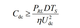
In this project, Udc=600V, the duty cycle D ranges from 0 to 0.88, PRL=5000W, due to the switching frequency of 40kHz, TS=25us, and ripple coefficient η Take 0.01 and input the value into the formula to obtain Cdc ≥ 30.5uF. In practical circuits, Cdc not only has filtering function, but also has certain energy storage function. Therefore, when setting parameters, it is generally necessary to obtain 5-10 times the calculated value. Therefore, the actual parameter value of 310uF/600V should be selected for the capacitor.
3.3 Selection of Boost circuit switching tubes
The Boost circuit switch uses MOSFET transistors with built-in reverse parallel diodes. Due to the presence of reverse parallel diodes, when manually connecting the solar panel in reverse, it can also provide a path for the reverse circuit, avoiding damage to the switch. According to the parameter requirements, the diode can withstand a maximum voltage of 600V and a maximum current of 30A in the circuit, which exactly meets the data setting of the diode model DSEI130-O6. Therefore, it is selected. When selecting MOSFET transistors, their rated voltage should be 1.5 times the output voltage of the photovoltaic panel, therefore 600 × 1.5=900V. The margin coefficient of the rated current should be 2 times, 30 × 2=60A.
4. Setting and selection of main components in inverter circuits
The selection of the inverter main circuit has been determined, and it is a solar inverter without a transformer structure. This project will specifically design and select the switching tubes and absorption capacitors in it.
4.1 Selection of switch components in the inverter main circuit
From the structure diagram of the inverter circuit, it can be seen that the main body of the circuit is mostly composed of switch components, so switch components are the core components of the inverter circuit. The commonly used switching components in practice are Mosfet (power field-effect transistor), IGBT (insulated gate transistor), and GTO (gate turnoff transistor). They each have their own applicable fields: Mosfet is generally used in some small capacity low-voltage systems; IGBT is suitable for medium capacity systems; In high-capacity systems, GTO is usually used. For this project, which is a 5kW solar photovoltaic power generation system and falls within the application range of IGBT, the switching components of the IGBT solar inverter circuit will be introduced here.
In the solar photovoltaic inverter circuit of this project, the maximum voltage that the C and E terminals of the IGBT may withstand is around 600V. Therefore, when selecting specific devices, IGBT tubes with a voltage resistance of 600V or above should be selected; In terms of current, the rated current should be around 30A for IGBT tubes. In addition, the switching frequency of this inverter circuit is 5kHz, and the IGBT itself will generate switching losses during the switching process, resulting in heat generation. The heating situation in this circuit may be more severe, so it is necessary to configure a heat dissipation device.
In summary, due to the specification limitations of IGBT tubes themselves, this project ultimately chose the model BMS35GB120DLC IGBT tube, which has a withstand voltage of 1200V and a peak current of 35A.
4.2 Design of LC filtering circuit parameters for output
According to the previous setting, if the frequency of the DC/AC switching tube is 5kHz, the period Ts is 200uS. Since the output voltage is between 200-600V, the average filtered output voltage is taken as 400V, and combined with the previous formula, L=1.6mH is obtained.
Similarly, assuming the ripple voltage coefficient of the capacitor is 0.01, combined with the previous formula, C=31.25 μ F. Among them, L is the power frequency inductance with a value of 1.6mH. To avoid noise generation, a closed iron core, such as an iron powder core, is selected. And C is the power frequency capacitor, which can be selected as 35 in size μ F.
4.3 Protective capacitance
In inverter circuits, due to the voltage spikes generated at the moment when the switching element is turned on and off, a protective capacitor needs to be connected in parallel at the switching element, and the protective capacitor capacity is generally relatively small. In this project, a switched capacitor C=3.3uF was selected, using the model CBB61-35uF-250VAC.