
In order to achieve the control objectives of the system, it is necessary to ensure that the system has superior control strategies, which are the core of the entire system. Reasonable, efficient, and stable control strategies can solve complex and tedious control problems.
The research on key technologies for portable mobile power systems is mainly divided into two parts. The first part focuses on the various charging methods of the system, and the control strategy of the designed charging module should meet the requirements of a wide range of voltage input and stable output voltage; The second part is aimed at the AC discharge process of the system. The inverter circuit in the designed AC discharge module needs to meet the stability and accuracy of the output voltage, and superior control strategies are needed to improve the anti-interference performance of the inverter output and reduce the total harmonic distortion rate of the output waveform.
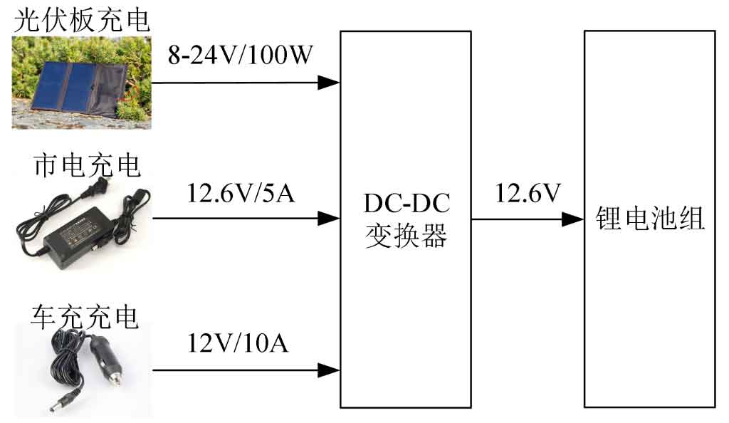
Due to its portability and mobility, the system usually needs to meet the needs of multiple charging methods. However, due to the different input voltages provided by different chargers to the system, as shown in Figure 1, it is necessary to use a DC-DC converter to increase and decrease the input voltage, and design a reasonable control strategy for control.
1. Basic topology of DC-DC
The DC-DC converter mainly consists of MOS transistors, energy storage components (inductors, capacitors), and a controller. By controlling the time ratio of MOS transistor conduction and cutoff, the ratio of output voltage to input voltage can be changed. Buck converter and Boost converter are the two most basic topologies in DC-DC converters, and other converter topologies are formed by their variations.
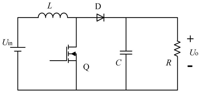
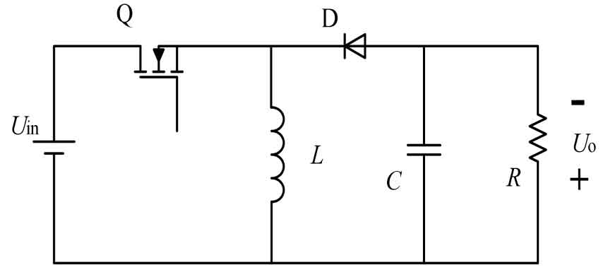
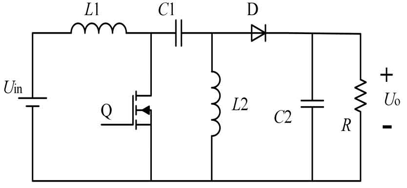
1.1 Buck converter
A Buck converter is a circuit structure composed of a voltage source, energy storage components, MOS switching tubes, and diodes, as shown in Figure 2.
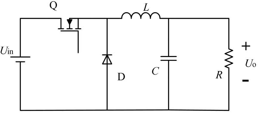
In a closed circuit, IL min is used to represent the minimum current flowing through inductor L, and IL max is used to represent the maximum current flowing through inductor L. When the MOS transistor Q is turned on, the current in L increases from IL min to IL min. When the Q transistor is turned off, the current in L continues through diode D. Assuming that the forward saturation voltage drop of the MOS transistor is ignored, the following equation can be derived when the Q transistor is turned on:
From this, it can be inferred that:
When the conduction state of the MOS transistor begins to cut off, due to the continuous power supply from the voltage source to L during the MOS transistor conduction period, the current in L reaches its maximum value. That is, when t=ton, the following equation can be listed:
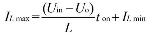
During the MOS transistor cutoff period, the current in L releases energy to the load through D, and the following equation is obtained:
When the MOSFET cutoff state terminates, the current in L gradually decreases from its initial maximum value to its minimum value, that is, when t=toff, the following equation is listed:
The joint formula yields:
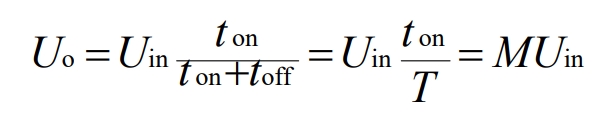
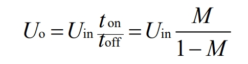
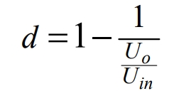
Among them, ton is the conduction time of the MOSFET within the same cycle, toff is the cutoff time of the MOSFET within the same cycle, T is the operating cycle of the MOSFET, and M represents the effective turn-on time within the same cycle, i.e Duty cycle: M=ton/T.
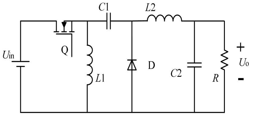
1.2 Boost converter
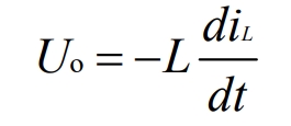
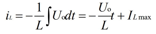
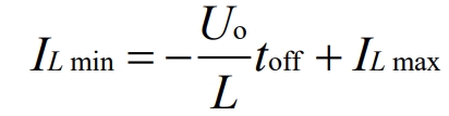
As shown in Figure 3, the Boost converter and Buck converter are the same on the components, but their placement is different. When the MOS transistor Q is conducting, energy is supplied to L through a closed circuit. At this time, diode D is reverse biased, and the energy of the load is provided by the filtering capacitor C. When the Q transistor is cut off, the current in inductor L begins to decrease. Due to the characteristics of the inductor components, inductor L will generate an induced electromotive force eL with opposite polarity to the conduction period of the Q transistor to prevent the current from decreasing. At this time, diode D conducts, and Uin and eL will simultaneously provide energy to the load and charge the capacitor.
When the Q tube is conducting, the voltage on inductor L is the input voltage Uin, and the current is Δ I/ Δ The rate of t=Uin/L increases linearly, during the ton period, the Q tube conducts, and the current increment in L is Δ I (+)=(Uin/L) ton. When the Q tube is cut off, the reverse voltage on L is Uo In, and the current in L is represented by Δ I/ Δ The rate of t=(Uo In)/L decreases linearly, and during the toff period, the Q transistor turns off, and the current in L decreases by Δ I (-)=(Uo In) toff/L, and the current increment in L during the steady-state ton period should be equal to the current decrease during the toff period, i.e Δ I (+)= Δ I (-), therefore:
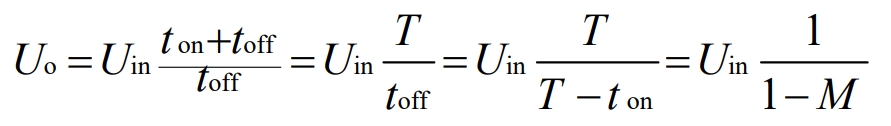
As can be seen from the above equation, by changing the duty cycle M, the ratio of input voltage to output voltage can be changed. Moreover, since M is always less than 1, the output voltage is always greater than the input voltage, so the converter plays a boosting role.
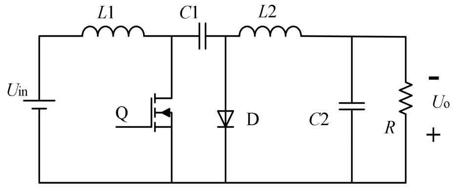
1.3 Buck Boost Converter
Buck type and Boost type converters can only achieve a single transformation effect, and their topological structures are cascaded and combined, as shown in Figure 4.
Remove the passive switch D1 in the Buck section and the active switch Q2 in the Boost section, and combine the inductance L1, L2, and capacitor C1 in the cross section to form a Buck Boost type converter, as shown in Figure 5.
The Buck Boost converter is different from the two converters mentioned above, as it can only operate in a single mode and can simultaneously achieve both boost and buck effects.
During the conduction period of MOSFET Q, the voltage on inductor L is Uin. Based on the above argument, it can be concluded that the current in L increases linearly at a rate of Uin/L. During ton, the Q tube conducts, and the current increment in L is Δ I (+)=(Uin/L) ton. When the Q tube is cut off, the current in L decreases linearly at a rate of Uo/L. During the toff period, the current in L decreases by Δ I (-)=(Uo/L) toff, and the current increment in L during the steady-state on period should be equal to the current decrease during the off period, i.e Δ I (+)= Δ I (-), therefore:
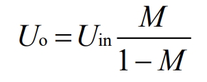
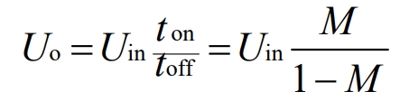
The duty cycle M is ton/T, and the expected output voltage can be obtained by changing M. When M=0.5, Uo=Uin; When M>0.5 and Uo>Uin, it is a boost type; When M<0.5 and Uo<Uin, it is a depressurization type.
1.4 Cuk converter
The Cuk converter is a topology structure obtained by dual transformation of the Buck Boost converter. Unlike the Buck Boost converter, the Cuk converter utilizes a current source and a voltage converter for energy output, as shown in Figure 6.
During the ton period, the MOS transistor Q conducts and L1 stores energy. C1 releases energy to RL through the Q transistor, C2, RL, and L2, and stores energy to L2 and C2. During the toff period, the Q transistor is turned off, and an electromotive force is induced on L1, causing the Q transistor to instantly rise from saturation voltage during conduction to a higher level. At this time, D conducts forward, and L1 charges and stores energy into capacitor C1 through C1 and D. At the same time, L2 releases energy to the load. This way, whether during the ton or toff period, energy is transmitted from input to output. During the toff period, capacitor C1 is used for energy storage charging. During the ton period, C1 releases the stored electrical energy to the load. C1 plays a role in energy storage conversion throughout the entire cycle, so it can be called a voltage converter. The input-output relationship can be derived from the formula in the above section:
1.5 Sepic and Zeta converters
The input and output relationship of Sepic converter and Zeta converter is the same. In Sepic circuit, the portable mobile power supply has continuous current but intermittent load current, which is beneficial for input filtering. In Zeta circuit, the portable mobile power supply has intermittent current but continuous load current. As shown in Figures 7 and 8.
The working principle of Sepic converter: During the ton period, the MOS transistor Q conducts, the Uin-L1-Q and C1-Q-L2 circuits conduct simultaneously, and L1 and L2 store energy simultaneously. During the toff period, the Q tube is turned off, and both the Uin L1 C1-D load and L2-D load circuits are conducting simultaneously. At this time, Uin and L1 both supply power to the load and charge C1 for energy storage. During the ton period, the energy stored by C1 will be released to L2 for transfer. The input-output relationship of the Sepic converter is:
Working principle of Zeta converter: During the TOFF period, the MOS transistor Q conducts, and Uin stores energy to inductor L1 through the Q transistor. At the same time, Uin and C1 jointly supply power to the load. During the TOFF period, the Q transistor turns off, and L1 stores energy and charges C1 through D. The input-output relationship of Zeta converter is:
From this, it can be seen that the Sepic converter and Zeta converter not only have the same input-output relationship, but also, The output voltage of both is also positive polarity.
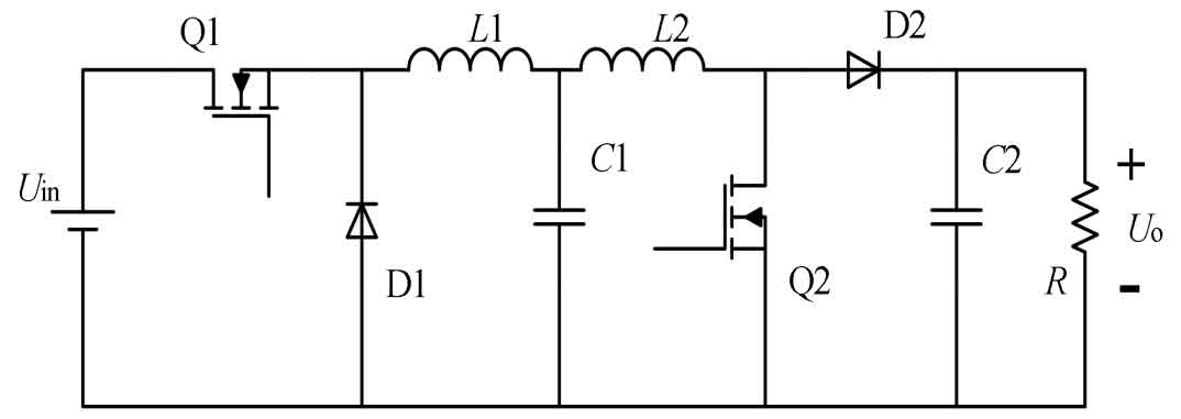
1.6 FSBB converter
Four Switch Buck Boost (FSBB) is a cascaded Buck Boost converter In the topology, a new structure is formed by combining passive components such as inductors and capacitors, and replacing rectifier diodes D1 and D2 with MOS transistors, which enhances the control of the topology structure, as shown in Figure 9.
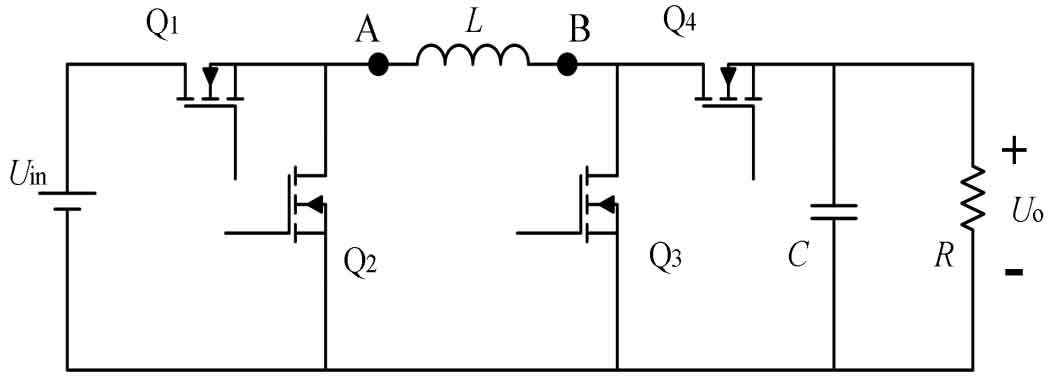
Under ideal conditions without considering dead time, the complementary driving waveforms of MOS transistor Q1 and Q2 form the Buck unit, while the complementary driving waveforms of MOS transistor Q3 and Q4 form the Boost unit. The Buck unit is based on the duty cycle d1 of Q1 transistor, and the Boost unit is based on the duty cycle d3 of Q3 transistor. The voltage at points A and B in the figure is:
When the FSBB circuit operates stably, the voltage at both ends of the inductor is equal, that is:
Combining the formulas yields:
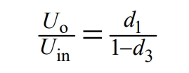
According to the formula, the ratio of output voltage to input voltage is based on two degrees of freedom d1 and d3. By controlling the values of d1 and d3, the range of input voltage can be expanded, and it has flexible adjustment performance.
According to the original intention of portable mobile power supply design, the product is commonly used in outdoor and emergency situations. During the charging process of photovoltaic panels, the input voltage is usually unstable due to the intensity of light, so a topology structure that can both boost and reduce voltage is needed to implement the DC-DC module part. The input and output polarity of Buck Boost and Cuk converters is opposite, while Sepic and Zeta converters have many passive components, which makes it difficult to achieve efficient control output. Therefore, this system adopts FSBB topology structure to achieve functionality.
2. FSBB three mode control strategy
2.1 FSBB Single Mode Control Strategy
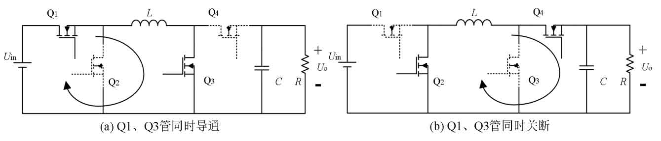
The most basic control method of FSBB is to switch the state of MOS tubes Q1 and Q3 simultaneously. When both are conducting at the same time, the switch tubes Q2 and Q4 of the same bridge arm will turn off, as shown in Figure 10 (a). The input voltage provides energy to inductor L for storage; When Q1 and Q3 transistors are turned off simultaneously, Q2 and Q4 transistors conduct simultaneously, as shown in Figure 10 (b). Inductor L outputs the stored energy to capacitor C and the load. This modulation mode is called single mode control, similar to the traditional Buck Boost topology, which only operates in a single mode. At this time, d1 and d3 are equal, equivalent to only being controlled by a single degree of freedom.
2.2 FSBB Dual Mode Control Strategy
According to the formula, d1 and d3 are the duty cycles of MOS transistor Q1 and Q3, respectively, and there are two control degrees of freedom, providing conditions for optimizing system control.
The traditional FSBB dual-mode control only has two states, namely boost mode and buck mode. When Uin>Uo, the system is in step-down mode. At this time, Q4 transistor is always on, Q3 transistor is always off, and d3 is 0. By adjusting the on/off time of Q1 transistor, the size of d1 can be changed to change the output input voltage ratio, similar to the basic Buck circuit topology, as shown in Figure 11 (a) and (b).
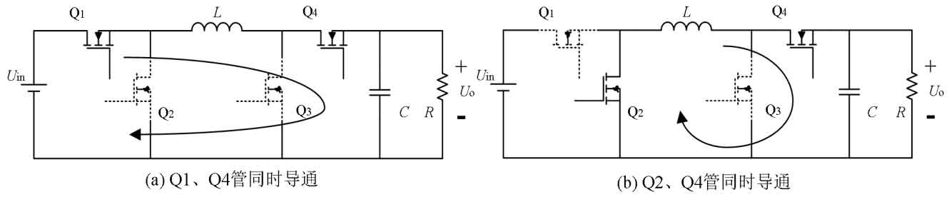
When Uin<Uo, the system is in boost mode. At this time, Q1 transistor is always on, Q2 transistor is always off, and d1 is 1. By adjusting the on/off time of Q3 transistor, the size of d3 can be changed to change the output to input voltage ratio, similar to the basic Boost converter circuit topology, as shown in Figure 12 (a) and (b).
2.3 FSBB Three Mode Control Strategy
From the above analysis, it can be seen that in order to meet the control requirements of rising and falling voltage, FSBB can set the rising or falling voltage mode by changing the on/off time of the switch tube. When Uin>Uo, Buck mode is used, and when Uin<Uo, Boost mode is used. However, in Uin æ Uo, the traditional dual-mode control strategy will create a transition blind spot, where the modulation state will switch back and forth between Boost mode and Buck mode, leading to a decrease in system stability.
Due to the practical effects of circuit wiring, noise interference, electronic component errors, etc., it is impossible to achieve a duty cycle d of 1 or 0, that is, there exists a maximum duty cycle and a minimum duty cycle. This article defines the maximum duty cycle involved in the experimental process as dmax and the minimum duty cycle as dmin. Therefore, 1-d1 and d3 can only take values within the range of [dmin, dmax].
In Buck mode, Q3 transistor is always turned off, Q4 transistor is always on, and the output input voltage ratio increases with the increase of Q1 transistor on time, making d=1-d1. By using the formula and d3=0, it can be inferred that:
In Boost mode, Q2 transistor is always turned off and Q1 transistor is always on. The output input voltage ratio increases with the conduction time of Q3 transistor, making d=d3. By using the formula and d1=1, it can be inferred that:
According to the formula, the output input voltage ratio is set to the x-axis and the duty cycle d is set to the y-axis. Figure 13 can be derived and drawn. Due to the limitation of the duty cycle between buck mode and boost mode, the output input voltage ratio between [m, n] cannot be taken, resulting in a modulation blind spot. To address this situation, this article proposes a third mode, namely the Buck Boost mode, for smooth transition.
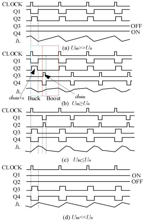
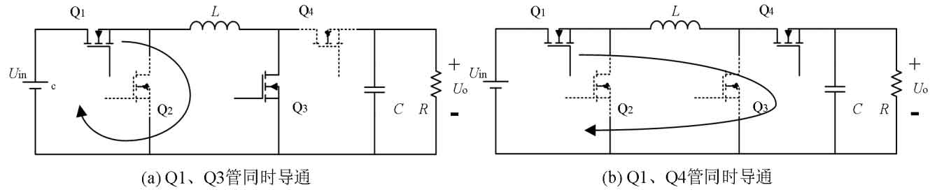
As shown in Figure 14 (a), when Uin>>Uo, the system operates in Buck mode. At this time, Q3 tubes are always off, Q4 tubes are always on, and Q1 and Q2 tubes perform complementary conduction with dead zones. Fix the output voltage of the converter and gradually reduce the input voltage of the converter. As L needs to store more electrical energy, the duty cycle d1 of Q1 transistor gradually increases, while the duty cycle d2 of Q2 transistor gradually decreases. At this point, d2 is an extremely important parameter. Due to the existence of a minimum duty cycle dmin in real systems, when d2 contracts to dmin, the internal logic chip receives MOS transistor signal information and begins mode conversion.
As the input voltage continuously decreases, when Uin ≥ Uo, in addition to complementary conduction of Q1 and Q2 transistors, Q3 and Q4 transistors also begin to perform complementary conduction with dead zones. At this point, it is equivalent to the Boost unit entering the Buck unit, forming the Buck Boost mode. When the Boost unit is cut in, d3 is cut in as dmin. In order to prevent output voltage jumping, d2 will be extended from dmin to dmin+x to offset the impact of d3 cut in. At this point, the Buck Boost mode is officially entered.
From Figure 14 (b), it can be seen that in one cycle, the first half can be seen as Buck mode, and the second half can be seen as Boost mode. When the input voltage continues to decrease, d2 will continue to decrease from dmin+x to dmin. At this time, the chip will perform logical conversion again. d2 will be fixed with the minimum duty cycle dmin, and d3 will jump out of the minimum duty cycle dmin and gradually increase. When Uin ≤ Uo, in one cycle, the first half is in Boost mode and the second half is in Buck mode, as shown in Figure 14 (c).
As the input voltage continues to decrease, when Uin<Uo, it will eventually enter Boost mode. At this time, Q1 transistor is always on, Q2 transistor is always off, and Q3 and Q4 transistors perform complementary conduction with dead zones, as shown in Figure 14 (d).