
Mobile power sources for laptops can greatly increase their battery life and are highly favored by some outdoor workers. However, there are shortcomings in the humanized design of traditional mobile power sources, such as fixed voltage. Laptops are different from mobile phones, and different models of laptops require different voltages. If the voltage remains constant, such a mobile power supply cannot meet the needs of most laptops. This article will optimize the adjustment problem of the output voltage of a DC-DC switching circuit step-down module, and assemble it into a mobile power supply that can switch multiple sets of voltage outputs to meet the battery life requirements of laptops with different input voltages.
1. Analysis of the working principle of the voltage reduction module
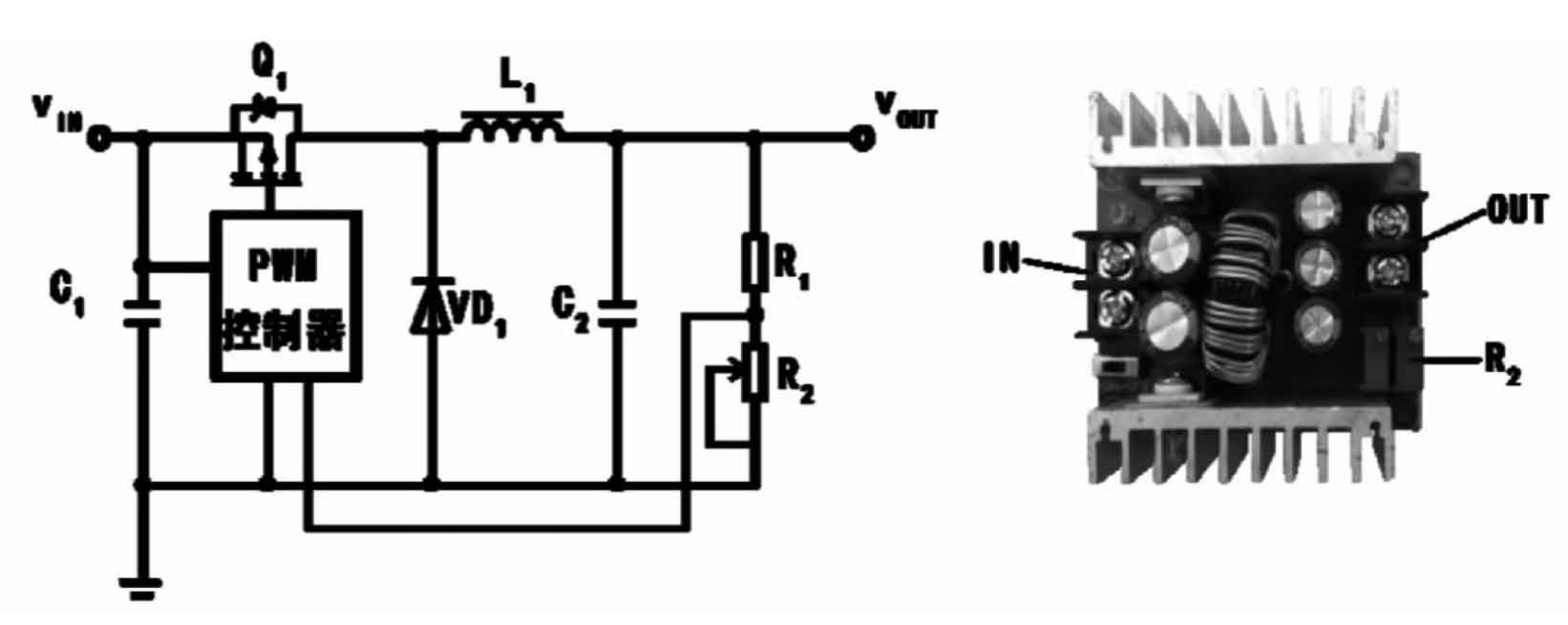
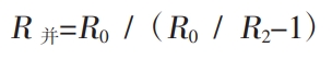
In order to better optimize and improve the output voltage of the DC-DC switching circuit step-down module, it is necessary to conduct a simple analysis of its step-down principle and voltage control method. Figure 1 shows the simplified circuit schematic and physical diagram of the step-down module. By adjusting the resistance value of R2, the output voltage can be changed.
1.1 Principle of voltage reduction
The voltage reduction principle of the DC-DC switching circuit voltage reduction module is as follows: In Figure 1, Q1 is an electronic switch. When it is closed, the voltage applied to both ends of the inductor is:
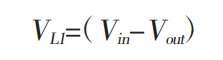
At this time, inductance L1 is excited by voltage VL1, and the increased magnetic flux of inductance is:
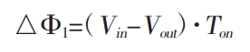
Where Ton is the Q1 closing time. When the electronic switch is disconnected, due to continuous output current, diode VD1 becomes conductive, inductor L1 is turned off, and the reduced magnetic flux is:
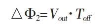
Among them, Toff is the Q1 disconnection time. Cycle:
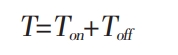
When the balance between the closed and open states of the switch is reached, the increased and decreased magnetic flux are equal, that is:
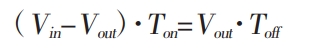
Due to the duty cycle:
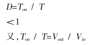
So Vin>Vout, in order to achieve voltage reduction.
1.2 Output voltage control
The function of PWM in the circuit shown in Figure 1 is to control the frequency and proportion of Q1 closure and conduction, thereby controlling the size of the output voltage Vout. The function of R1 and R2 is to provide a feedback signal for the output voltage. The PWM controller automatically adjusts the switching speed and duty cycle of Q1 based on the feedback signal to achieve stable voltage output. R2 is a variable resistor, which adjusts the size of R2 to change the feedback signal and thereby adjust the output voltage.
2. Analysis of Output Parameters of Notebook Adapters
Measure and analyze the actual output voltage of the laptop power adapter to determine the accurate value of the mobile power output voltage. Most laptops on the market have voltages of 19V, 19.5V, and 20V, while some laptops have voltages of 15V, 16V, and 18V. Some miscellaneous laptops also have voltages of 9V and 12V.
Taking the mechanical revolution notebook with an input voltage of 19V and a power of 120W as an example for experimental analysis, it was found that its actual value is not accurate at 19V. Measurement has found that the adapter of this model of laptop has an actual output voltage of 19.29v without load. During the operation of a laptop, its output voltage often fluctuates around 19V. As shown in Table 1:
| Measurement frequency | Standby voltage (v) | Office voltage (v) | Ps plotting voltage (v) | High Performance Playing Large Game Voltage (V) |
| 1 | 19.13 | 19.07 | 19.07 | 18.97 |
| 2 | 19.12 | 19.10 | 19.03 | 18.98 |
| 3 | 19.13 | 19.08 | 19.05 | 19.02 |
| 4 | 19.12 | 19.11 | 19.05 | 19.01 |
| Average value | 19.12 | 19.09 | 19.05 | 18.99 |
According to the table, it can be seen that the output voltage of the laptop will be pulled down during operation. There are two reasons: firstly, the voltage divider effect of the power cord connecting the laptop to the power adapter; The second reason is due to the motherboard of the power adapter. The output voltage of a typical power adapter is relatively stable, with a difference of less than 0.1v from the output voltage when unloaded. Therefore, the main reason for the voltage drop is due to the resistance of the power cord connected to the laptop by the power adapter.
3. Research on module output voltage regulation
After the previous measurement, it can be found that the actual output voltage of the power adapter is about 0.3v higher than the standard voltage, in order to offset the voltage loss of the power line connecting the power adapter to the laptop. Based on the power supply voltage of laptops in daily life, seven sets of voltages, 9V, 12V, 15V, 16V, 19V, 19.5V, and 20V, are taken as the standard output voltage for mobile power supplies. The corresponding actual values should be 9.30v, 12.30v, 15.30v, 16.30v, 19.30v, 19.80v, 20.30v.
3.1 Design of Resistance Switching Circuit
Use a screwdriver to adjust R2 in module 1, and adjust the output voltage to 9.30v, 12.30v, 15.30v, 16.30v, 19.30v, 19.80v, and 20.30v in sequence. Measure the corresponding R2 resistance values, as shown in Table 2.
| Standard voltage (v) | Select voltage (v) | R2 resistance value (KΩ) |
| 9 | 9.30 | 25.7 |
| 12 | 12.30 | 35.3 |
| 15 | 15.30 | 44.9 |
| 16 | 16.30 | 48.1 |
| 19 | 19.30 | 57.6 |
| 19.5 | 19.80 | 59.2 |
| 20 | 20.80 | 60.80 |
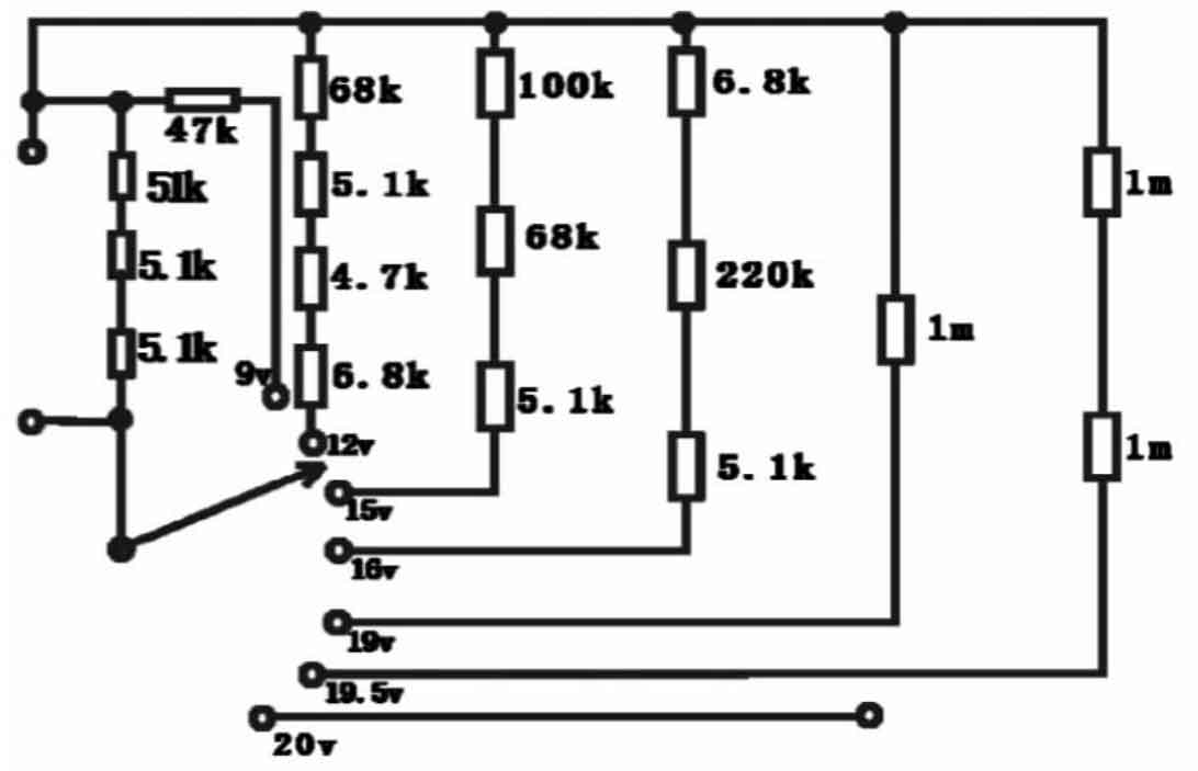
The resistance values of the 7 sets of R2 sliding resistors measured in Table 2 can theoretically be obtained by replacing the position of the variable resistor R2 in the module with 7 fixed resistors with resistance values of 25.7 Ω, 35.3 Ω, 44.9 Ω, 48.1 Ω, 57.6 Ω, 59.2 Ω, and 60.8 Ω. The switching outputs of the 7 sets of voltages, 9v, 12v, 15v, 16v, 19v, 19.5v, and 20v, can be obtained. Design a resistance switching circuit as shown in Figure 2.
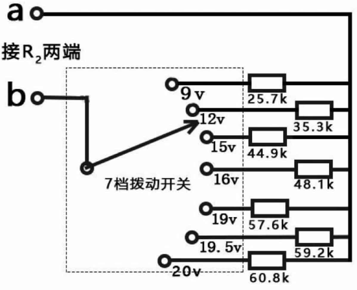
The terminals a and b in Figure 2 are connected to the two ends of the variable resistor R2 in Module 1, which is equivalent to replacing R2 with the circuit in Figure 2. The dashed area in the figure represents the 7th gear toggle switch. By switching the toggle switch gear, R2 can be replaced with one of the fixed resistance values shown in the figure, which is 25.7 Ω, 35.3 Ω, 44.9 Ω, 48.1 Ω, 57.6 Ω, 59.2 Ω, and 60.8 Ω, to obtain the corresponding output voltage.
But there are two problems with the circuit in Figure 2: firstly, the existing single resistor does not have the required resistance value; The second is that at the moment when the circuit switches from the previous resistor to the next resistor, both ends of R2 are disconnected, resulting in an infinite resistance value of R2. As shown in Figure 1, if the resistance value of R2 is infinite, the feedback voltage will increase to the output voltage, which will damage the module due to excessive feedback voltage.
Therefore, further research is needed if the circuit in Figure 2 is to be applied in practice.
3.2 Improvement of Resistance Switching Circuit
The voltage of the laptop is between 18V and 20V, and it can also be used if it differs from the standard voltage by about 1V. In the process of series parallel connection with a limited number of fixed resistance values, it is impossible to obtain the accurate resistance value that people want, and can only be as close as possible. But as long as the output voltage deviation is ensured to be 1v, the laptop can be powered normally.
| Standard voltage Vout (v) | Select voltage (v) | R2 theoretical resistance value (kΩ) | Theoretical value of R (kΩ) | R and actual value (kΩ) | R2 actual value (kΩ) | Actual output voltage Vout (v) | Absolute error △ Vout (v) |
| 9 | 9.30 | 25.7 | 44,31 | 47 | 26.58 | 9.58 | 0.58 |
| 12 | 12.30 | 35.3 | 83.41 | 68+5.1+4.7+6.8=84.6 | 35.51 | 12.42 | 0.42 |
| 15 | 15.30 | 44.9 | 168.58 | 100+68+5.1=173.1 | 45.23 | 15.45 | 0.45 |
| 16 | 16.30 | 48.1 | 224.71 | 6.8+220+5.1=231.9 | 48.42 | 16.46 | 0.46 |
| 19 | 19.30 | 57.6 | 979.20 | 1000 | 57.67 | 19.38 | 0.38 |
| 19.5 | 19.80 | 59.2 | 1811.52 | 1000+1000=2000 | 59.38 | 19.89 | 0.39 |
The circuit shown in Figure 3 is an improved resistance switching circuit, which uses a common resistor in parallel to solve the problem of burning the motherboard due to the infinite resistance value during the switching process in Figure 2 circuit. The series part of the three resistors 51k, 5.1k, and 5.1k is the common resistor, denoted as R0=61.2k. When the switch is turned to the 20k terminal, it is not connected in parallel with any resistance, and the resistance values at both ends of a and b are R0=61.2k. When the output voltage in Table 3 is 20v, the corresponding R2=60.8k resistance value is similar. Replacing R2 with R0 yields an output voltage of 20.45v, which differs from the standard voltage of 20v by 0.45v and does not exceed 1v. Therefore, R0=61.2k can be used as the resistance value corresponding to the 20V output of the mobile power supply. The larger R2, the greater the output voltage, and the total resistance value decreases when a resistor is connected in parallel with other resistors. Therefore, we choose the resistance value corresponding to an output voltage of 20V as the common parallel resistor. To obtain the R2 resistance values corresponding to the other sets of output voltages, simply connect a resistor with a certain resistance value in parallel. According to the data of R2 in Table 2 and the size of R0, the resistance values corresponding to the parallel connection with R0 for the six output voltages of 9v, 12v, 15v, 16v, 19v, and 19.5v when the voltage is higher than 0.3v can be calculated, denoted as R and, as shown in Table 3. The circuit shown in Figure 3 is composed of a constant resistance that is approximately equal to R.
By:
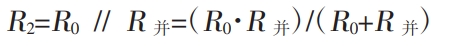
Obtain:
R2 actual value=R0//R and actual value

The formula can be used to calculate the theoretical value of R, the actual value of R2, and the absolute error in Table 3.
The absolute error of the actual output voltage data in Table 3 does not exceed 0.4v, which is much lower than 1v. Therefore, it can be considered that replacing the variable resistor R2 of the step-down module with the circuit shown in Figure 4, which is composed of R0 and the actual values of each R, will not affect the normal operation of the laptop by supplying power to the corresponding output voltages.
The actual resistance switching circuit is shown in Figure 3. By turning the switch to 7 different positions, R2 is switched to different resistance values, resulting in 7 different output voltages of 9v, 12v, 15v, 16v, 19v, 19.5v, and 20v.
4. Analysis of the overall assembly system of mobile power supply
Figure 4 is a schematic diagram of the overall circuit system of the mobile power supply. From left to right, there are 7 series of rechargeable high rate lithium batteries, voltage balancing module, simplified circuit of DC-DC switching circuit step-down module (corresponding to module 1 in Figure 1), and resistance switching circuit. The dotted line represents the 7th gear toggle switch, which switches seven sets of resistors R and obtains seven sets of output voltages: 9v, 12v, 15v, 16v, 19v, 19.5v, and 20v. The functions of the voltage balancing module include: overcharging and discharging protection for lithium batteries, and voltage balancing control for seven series lithium batteries. When supplying power to different laptops, simply switch the voltage to the required voltage for the corresponding laptop, and connect the laptop charging interface to the Vout output terminal with a power cord.
5. Summary and Outlook
Through the above theoretical and experimental research, the assembled mobile power supply has superior performance and higher compatibility. Significant advantages in practical applications:
Capable of switching output voltage, strong load capacity, extended battery life, and high safety factor. In addition, in terms of system structure, this article uses 7-series, 24V lithium batteries for power supply, which reduces the current carried by the motherboard compared to the market 12V under the same power conditions. The same cost can achieve higher power output, which also provides a new approach for the production and research of laptop mobile power supplies.
The inspiration from improving this mobile power supply is that firstly, it belongs to the assembly of multiple modules internally. Some input and output components, interfaces, switches, motherboards, lithium battery voltage balancing modules, etc. can be integrated together through some processes to reduce production difficulty; Secondly, the outer shell of this power supply is made of waterproof box milled holes. Through the design of the appearance and the method of injection molding, the appearance can be improved to enhance its aesthetics, the internal structure can be optimized to enhance its stability, and the volume can be compressed for easy portability. Through these two major improvements, the difficulty of quantitative production can be reduced, and production costs can be further reduced.