
Mobile power supply is a portable charger that provides power to devices such as mobile phones through its internal stored energy. The research direction of mobile power sources focuses on daily life and commercial use, aiming to provide power to devices such as mobile phones and achieve a voltage output of 5V. At present, research on mobile power sources is developing towards multifunctional directions. Gu Jianning et al. designed a mobile power supply that combines solar charging and manual charging, and added practical auxiliary functions such as LED lighting. Wu Xuejun et al. designed a DC-DC boost mode mobile power supply and selected a low-power microcontroller as the core control system. Ding Chenggong and Wang Shenghong designed a mobile power supply with a power management chip as the core component, which is powered through a USB interface or a 5V adapter. Some mobile power sources also have the function of increasing their own charging current.
Workers in forestry, civil engineering, surveying and mapping industries use different types of equipment outdoors for a long time (such as handheld GPS, data collectors, water levels, wood moisture content detectors, etc.). When the power of the equipment is insufficient, work efficiency and testing time will be seriously affected. The current mobile power supply cannot provide power to devices with batteries installed, and cannot provide the corresponding power supply voltage for devices that use charging methods. Based on this, by analyzing the different power supply methods and input voltage requirements of outdoor small professional equipment, multiple ways of endurance power supply are realized. Multiple circuit protection and overall protection measures for mobile power supply are designed according to the outdoor working environment, which can facilitate the work of outdoor workers and improve work efficiency.
1. Overall structural design
The overall structural design of mobile power supply is divided into two parts: external design and control circuit design. The external components of the mobile power supply include: USB charging interface for lithium batteries, solar panel, multifunctional output module, DC terminal output part, and external practical structural design. The internal control circuit design of mobile power supply includes: voltage input part, microcontroller control system, voltage regulation circuit part, voltage stabilization circuit part, and protection circuit part.
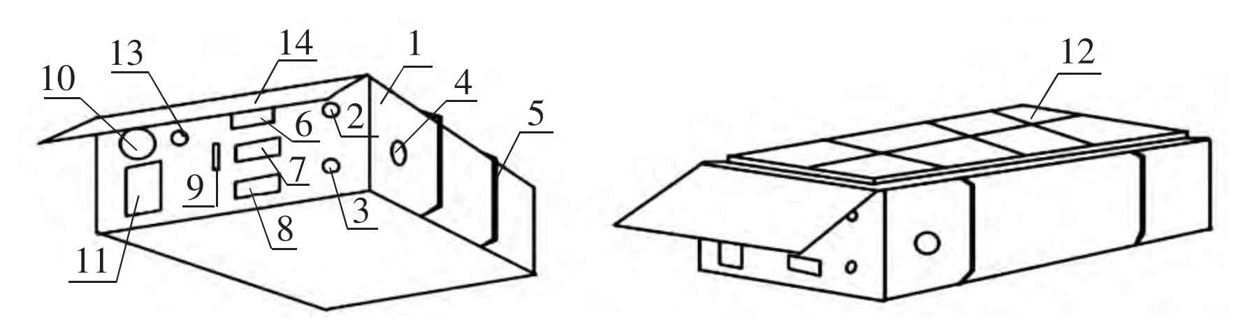
The external design of the mobile power supply first involves charging the lithium battery through the USB interface, as shown in Figure 1. The power is input through the charging port (9), and linear charging is adopted. Through the internal mains rectifier module of the mobile power supply, the 220V mains voltage is reduced and rectified using a step-down transformer and rectifier bridge circuit. This feature has a certain degree of universality and is suitable for daily power input of mobile power sources. The solar panel (12) absorbs sunlight and converts it into electrical energy through an internal solar photovoltaic module, which is stored in a lithium battery. This structure is designed for the special conditions of forestry workers working outdoors, and can achieve outdoor charging and emergency power supply. The multifunctional output module includes a 3.3V voltage output port (6), a 5V voltage output port (7), and a 12V voltage output port (8), which are regulated and output through an internal 5V-12V voltage regulation circuit and a 5V-3.3V voltage regulation circuit. This structure voltage is designed for small outdoor forestry instruments, meeting the needs of most small outdoor forestry instruments. The output part of the DC terminal is controlled by the voltage adjustment button (13) to select voltage within the range of 3.3 V to 12 V in the Sepic converter circuit of the switching power supply topology, and output is carried out through the positive terminal (2) and negative terminal (3). This structure is designed for small outdoor forestry instruments with batteries installed. Finally, it also includes practical structures such as a data cable lighting fixture (4), a data cable fixing device (5), a liquid crystal display (11), and a silicone protective cover (14).
In the internal control circuit of the mobile power supply, the voltage input part includes a solar power generation module and a mains rectification module, which realizes the input of voltage and rectification of different voltages to a fixed 5 V voltage; The microcontroller control system consists of an STC89 C52 RC microcontroller and an analog-to-digital conversion module, achieving overall control of the voltage regulation circuit; The voltage regulation circuit section includes a 5V to 12V voltage regulation circuit module that supplies power to the multifunctional output module, a 5V to 3.3V voltage regulation circuit module, and an adjustable circuit section that supports manual voltage regulation of DC terminals; The voltage stabilizing circuit adopts the LM2596 chip, which plays a role in overall voltage stabilization; The protection circuit mainly includes the overcharge and discharge protection circuit of the battery to prevent deformation and leakage of the battery.
2. Mobile power supply control circuit design
2.1 Voltage input section
2.1.1 Solar photovoltaic power generation
There is a concentration difference between electrons and holes at the junction of the P-N layer in semiconductors. Under the irradiation of sunlight, new hole electron pairs are generated. At the same time, under the action of the internal electric field force, holes in the N region drift towards the P region, and electrons in the P region drift towards the N region, causing a large amount of negative and positive charges to accumulate in the N and P regions respectively. There is a potential difference on the P-N junction, and current is generated when the circuit is connected.
When the lighting conditions are suitable, solar panels absorb sunlight and convert solar energy into electrical energy. Due to the inability of the solar energy output voltage to be directly applied to forestry equipment, the voltage of 9 V was adjusted to 5 V. The voltage conversion circuit is shown in Figure 2.
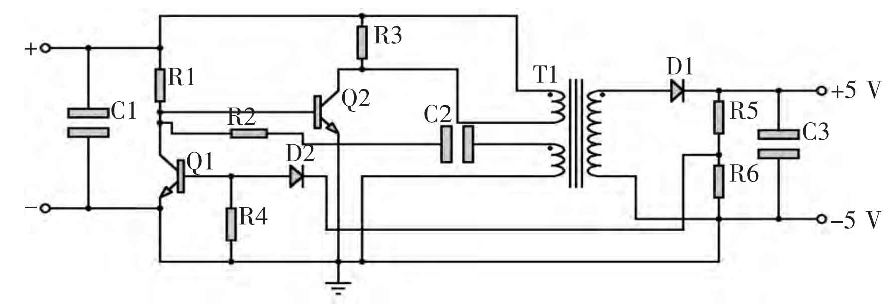
The transistor Q2 is a common beam amplifier. When it is conducting, the voltage of high-frequency transformer T1 is ① positive and ② negative, and the voltage directions at both ends of the transformer are opposite, that is, ③ negative and ④ positive. At this time, the left end of rectifier diode D1 is negative and in the cut-off state, and the battery is not charging. The transistor Q1 is also a common beam amplifier, and when it cuts off, the voltage direction at both ends of the transformer is the same, that is, positive ③ and negative ④. The rectifier diode D1 is in a conductive state and is rectified by the capacitor C3. This method can continuously, stably, and steadily store electricity in the battery.
2.1.2 mains rectification
The mains power module adopts a combination of a step-down transformer and a rectifier bridge to convert 220 V mains power into lower DC power. The peak to peak AC voltage that has been reduced by the step-down transformer is 28.736 V. Then, the AC power is converted into DC power through the rectifier bridge, and the voltage is rectified to 8 V. Then, the RC filtering circuit is used to reduce the AC component, filter out the ripple of the rectified output voltage, and send the DC voltage to two series connected LM7824 three terminal voltage regulators to output a stable 5 V DC voltage, which is ultimately connected to the protection circuit.
2.2 Microcontroller control system
The microcontroller control system adopts a low-power and high-performance CMOS 8-bit STC89C52 RC microcontroller, which includes 8k bytes of Flash, 512 bytes of RAM, 32-bit I/O port lines, built-in 4KB EEPROM, MAX810 reset circuit, 3 16 bit timers/counters, 4 external interrupts, a 7-vector 4-level interrupt structure compatible with the traditional 51 5-directional 2-level interrupt structure, and a full duplex serial port. Due to the complexity of the external clock circuit, self-excited oscillation is used. The clock circuit pins XTAL1 and XTAL2 are externally connected to a quartz crystal oscillator, causing the internal oscillator to oscillate at a quartz crystal oscillator frequency of 12 MHz, generating a clock signal; Both the internal and external program memory of the C52 microcontroller require CPU access, allowing the input EA to be connected to a high level for opening the main interrupt switch; After connecting the bidirectional I/O port with a pull-up resistor, it is connected to the output port of the ADC0808 chip to output the corresponding digital signal; The bidirectional I/O port P2.0 outputs a PWM square wave, which is controlled by a driving circuit composed of an IR2101 chip to turn on or off the switch IGBT in the adjustable voltage circuit, thereby achieving voltage regulation.
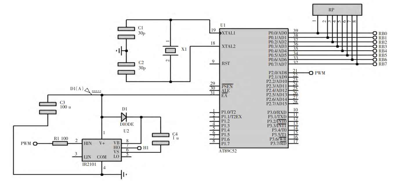
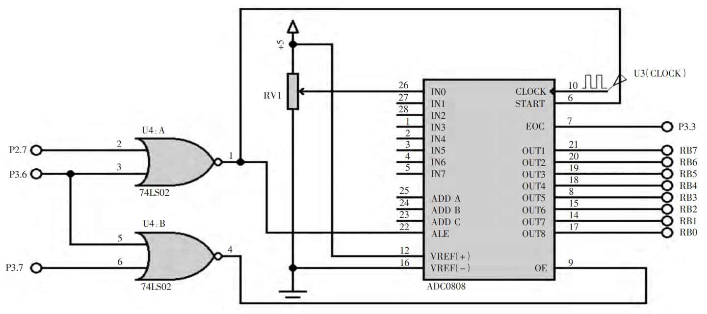
However, the STC89 C52 RC microcontroller does not include an A/D conversion module. An analog-to-digital conversion module needs to be added to convert the input voltage into a digital signal, allowing the microcontroller to read data information and control external circuits. The A/D conversion part uses ADC0808 chip to convert analog signals into digital signals and transmit them to the microcontroller. The ADC0808 chip is a conversion chip that includes an 8-bit A/D converter, 8-way multiplexer, and uses a progressive approximation. Its accuracy is 1/2LSB, and the power consumption is 875 mW at a temperature of 25 ℃. The conversion time depends on the chip clock frequency. When CLK=500 kHz, TCONV=128 us. In this design, the minimum system has 40 pins connected to a 5V power supply to provide voltage for the digital circuit, and 20 pins grounded to provide ground level; Connect the P0 pin to a pull-up resistor and then drive the analog-to-digital conversion module, which is used to control the mutual conversion between analog-to-digital; X1 and X2 pins are connected to a quartz crystal oscillator to provide clock signals for the operation of the microcontroller; Connect three voltage conversion modules to each P1 port; P21 port is connected to the reset pin; P3.5T1 external USB interface; P3.6/3.7 External RAM read/write memory is connected to the analog-to-digital conversion chip through an OR gate, respectively. The pins of the microcontroller are shown in Figure 3, and the conversion module circuit is shown in Figure 4.
2.3 Voltage regulation circuit section
2.3.1 Voltage regulation circuit section from 5 V to 12 V
The 5 V to 12 V voltage regulation circuit uses a in-phase amplifier to amplify the input 5 V voltage to 12 V. To ensure stable voltage output, capacitors C1 and C2 are connected between input and output and ground to avoid the impact of voltage fluctuations caused by voltage stabilization. Resistance R2 is used as the balance resistance, and a balance resistance value of 33 k Ω is selected. The amplification factor of the output voltage is controlled by adjusting the ratio of the positive phase input resistance R1 to the feedback resistance Rf. In the amplification circuit of the same phase amplifier, the Uo=(1+Rf/R1) Ui relationship is satisfied. The input Ui is 5 V constant voltage DC, and the output is 12 V constant voltage DC. To ensure the stability of the output voltage, the feedback resistance needs to be as large as possible. Therefore, if Rf=140 k Ω, the corresponding R1=100 k Ω is selected. To reduce the output impedance and achieve impedance matching, an emitter follower is added after the amplification circuit, while also serving as a buffer.
2.3.2 Voltage regulation section from 5 V to 3.3 V
The voltage regulation circuit between 5 V and 3.3 V uses a three terminal linear step-down chip AMS1117 with low output voltage difference, which reduces the input 5 V voltage to a fixed voltage of 3.3 V for output. The AMS1177 chip integrates overheating protection and current limiting circuits internally, eliminating the need for additional overcurrent protection circuits. AMS1177 operates at a 5 V DC voltage, driven by a 5 V DC power supply connected to the input IN pin to drive the chip; GND pin grounding provides a ground level for the chip; Parallel connection of 10 uF electrolytic capacitor and 100 nF ceramic capacitor at the input and output terminals ensures stable input and output voltage. When the load current exceeds 1.2 A or the circuit temperature exceeds 140 ℃, the overcurrent protection circuit operates to ensure the safety of the chip and system.
2.3.3 Adjustable voltage section
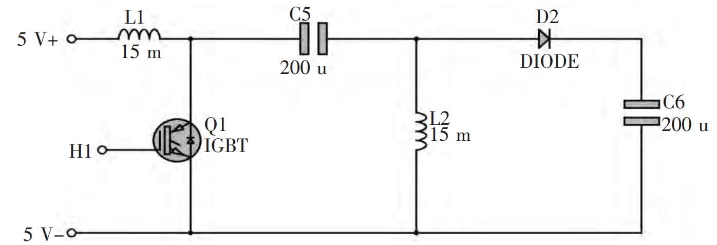
The adjustable voltage part adopts a switching power supply topology structure Sepic conversion circuit. When the cycle is constant, the duty cycle can be changed by changing the pulse width to achieve boost and buck [13]. In terms of devices, fully controlled transistor IGBT and Schottky diode are selected. IGBT combines the advantages of GTR and MOSFET [14], not only has strong current capacity, but also has fast switching speed and good thermal stability; Schottky diodes have low conduction loss and high efficiency, and can effectively improve voltage conversion efficiency as freewheeling diodes. The basic circuit is shown in Figure 5. Within one cycle, when the switch T is closed, the power supply charges the inductor L1, while the coupling capacitor C1 charges the inductor L2. The positive pole of the freewheeling diode D shows a negative voltage and cuts off, and the filtering capacitor C2 has the same voltage as the load at both ends; When switch T is disconnected, inductor L1 charges the coupling capacitor, freewheeling diode D conducts, inductor L2 supplies power to the load, and the average output voltage can be expressed as Vout=(ton/toff) Voff. In this design, the circuit input is a 5V voltage after mains or photoelectric rectification. The PWM square wave output by the timer of the C52 microcontroller is driven by the circuit to adjust the duty cycle, thereby controlling the opening and closing of the IGBT and ultimately achieving the effect of controlling the output voltage.
2.4 Voltage stabilizing circuit section
The LM2596 chip is used in the voltage stabilizing circuit. LM2596 is a commonly used high current switching regulator chip, with a maximum output current of 3 A, and the heat generated when outputting high current is much smaller than that of a linear regulator IC. The 5 pins of LM2596 are the turn off control terminals, which are effective at low levels. During normal operation, ground the 5 pins. After the voltage stabilization circuit is connected to the load detection circuit, when the load stops working, the detection circuit outputs a high level, which is sent to pin 5 of LM2596 to close its output terminal, thereby putting the entire circuit in an ultra-low power consumption state. The static power consumption is only 80 uA, making the entire circuit more stable. 1 pin is connected to a 5V input voltage through an electrolytic capacitor to provide voltage to the chip, 3 pins share ground with 5 pins to provide ground level, 2 pins stabilize voltage through reverse diodes and electrolytic capacitors, thereby achieving overall voltage stabilization. 4 pins form a feedback network with the input and output terminals to maintain the overall stability of the voltage stabilization circuit. The output end of the voltage stabilizing circuit can use USB female port output or terminal output to meet various device interface requirements.
2.5 Protection circuit section
2.5.1 Overcharge protection circuit
The overcharge protection circuit is connected to the voltage regulation circuit to test the current of the voltage regulation circuit. The voltage input part charges the battery through the normally closed contact of contactor K1. When the battery voltage in the overcharge protection circuit is greater than the overvoltage setting value, the coil M of contactor K1 attracts and opens the normally closed contact, thereby disconnecting the photovoltaic mains input module from the battery and achieving overcharge protection. The circuit is shown in Figure 6.
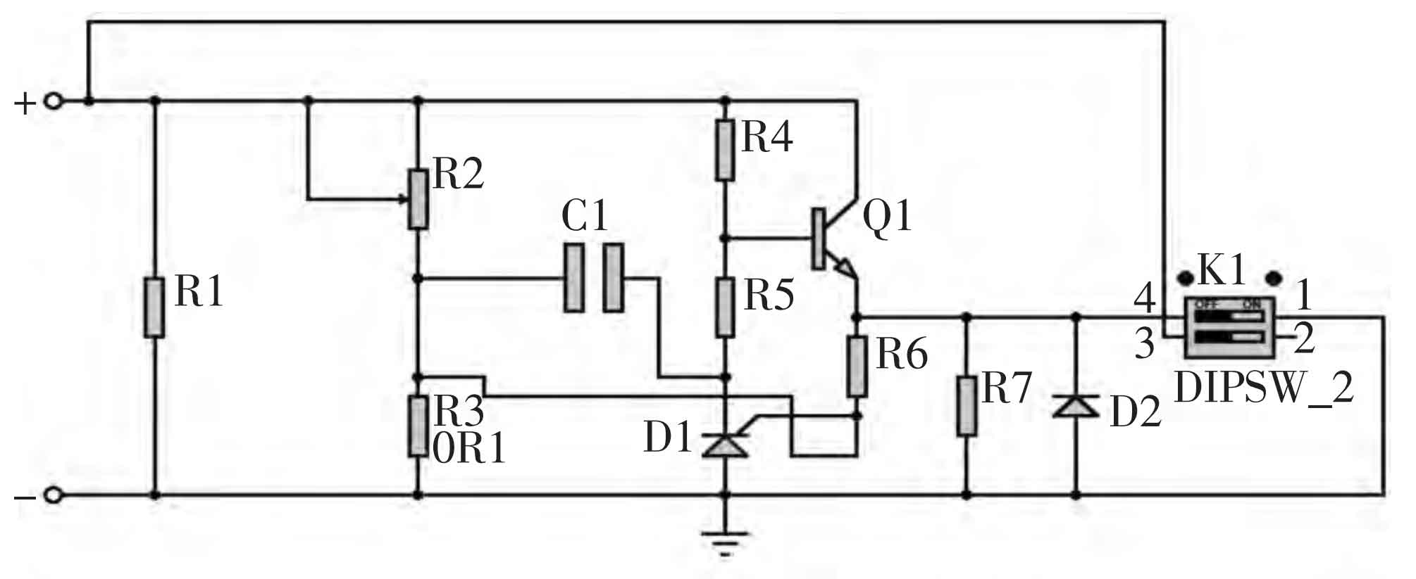
2.5.2 Overdischarge protection circuit
When the battery voltage is greater than the undervoltage setting, the contactor K2 coil M closes, closing the normally open contact to provide DC power to the output part. When the battery voltage is lower than the undervoltage setting, the contactor coil M does not close, and the normally open contact returns to the disconnected state. The battery stops providing DC power to the output part, achieving over discharge protection.
3. Software simulation and verification
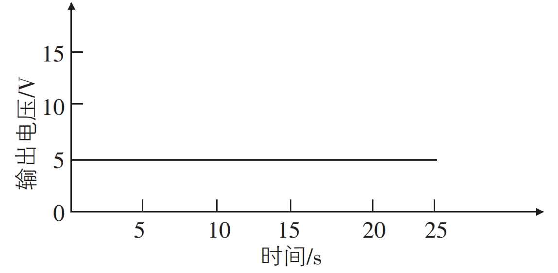
The circuit is simulated using Multisim14.0 to verify its correctness. The 220 V sine AC power is isolated by a transformer and then flows through a single-phase rectifier bridge. The input voltage u2 is rectified at a positive half cycle wt=0, and the rectified voltage ud=u2 passes through the conduction angle θ After time, ud decreases until the reverse voltage is positive half cycle wt=0, becoming a positive phase biased DC voltage. The input AC waveform is a standard sine wave, which is rectified and becomes a half wave that only exists on the positive half axis; After capacitor filtering, it becomes a stable constant DC output, and the voltage waveform is a stable straight line parallel to the x-axis. The voltage of solar energy after photoelectric conversion is 9 V. In order to ensure its continuous and stable application in forestry equipment, a common beam amplifier and a high-frequency transformer are used to store the voltage after voltage reduction in the battery. The output is the same as the rectification result of the mains power, and the waveforms of both are shown in Figure 7.
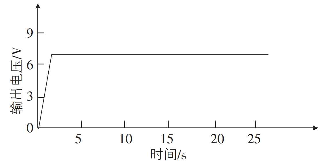
The waveforms of 5 V to 3.3 V, 5 V to 12 V, and adjustable voltage are similar. The input voltage is a constant 5 V DC parallel to the x-axis, and the output voltage is a constant DC voltage. The waveforms are straight lines parallel to the x-axis, with amplitudes of 3.3 V and 12 V, respectively. Due to the simplicity of the first two constant voltage regulation methods, only more complex adjustable voltage waveforms are included. When the trigger pulse arrives, the gate trigger takes time, so there is a brief rising edge at the beginning of the voltage waveform when the trigger first arrives, and then it rises to the expected output voltage, such as 7.5 V. After that, the output voltage stabilizes at 7.5 V. The waveform is a straight line parallel to the x-axis, as shown in Figure 8. Through the control of the microcontroller, a PWM wave is output, but the square wave output by the microcontroller cannot directly drive the field-effect transistor, It is necessary to control the field-effect transistor after passing through the driving circuit, adjust the duty cycle to adjust the on/off time of the IGBT and achieve voltage regulation.
After the 220 V sine AC voltage is reduced by a transformer, the peak to peak voltage that has been reduced is 28.736 V. It then flows through a single-phase rectifier bridge and becomes a positive biased DC voltage; After being filtered by capacitors, it becomes a stable constant DC output. After the photovoltaic conversion circuit, the output of solar energy is also a stable and constant DC output, and the waveform meets the expected setting requirements.
4. Conclusion
The design of a multifunctional mobile power supply system for small outdoor professional equipment described in this article includes a multifunctional output module, a DC terminal output section, and various practical devices to achieve a stable DC 5 V voltage input for solar photovoltaic power generation with an input voltage of 8 V and a supply voltage of 220 V. On the voltage regulation circuit, the 5-V voltage is adjusted to a stable output of 3.3V using a three terminal linear step-down chip AMS1117, and the boost output is adjusted to 12V using a in-phase amplifier amplification circuit. The STC89 C52 RC microcontroller and analog-to-digital conversion module form a microcontroller control system to achieve voltage regulation output within the range of 3.3V to 12V. To provide voltage supply of 3.3 V and 12 V for different outdoor small forestry equipment, and to achieve adjustable voltage output within the range of 3.3 V to 12 V through DC terminals, providing power to devices using batteries and enabling continuous power supply for devices with different charging methods. At the same time, a voltage stabilizing circuit and a protection circuit are set up to achieve stable and safe output. The feasibility and rationality of this design scheme have been verified through simulation experiments on the adjustable voltage section and rectification section, which can be widely used.