
The function of a solar grid connected power generation system is to convert the electricity generated from photovoltaic cells, which is not stored by batteries, but directly sent to the grid through grid connected inverters. The overall framework of the power generation system and the functions of each module will be discussed.
1. Functional structure of solar photovoltaic grid connected system
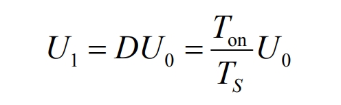
This project is a 5kW household solar grid connected power generation system. Its main body is composed of a control circuit and a main circuit,.
This functional diagram includes the control circuit and main circuit in the solar photovoltaic grid connected power generation system. The main power supply consists of inverters, DC/DC conversion circuits, and photovoltaic cell arrays. The function of the main circuit is to convert solar energy into electrical energy. Here, the role of the DC/DC converter is to convert the lower voltage level DC energy output by the solar photovoltaic cell into higher voltage level DC energy. Then, the DC energy of that level is passed through the inverter, and finally, it outputs grid connected AC energy; The DSP controller, electrical energy detection unit, fault detection unit, driving circuit, and protection circuit in the control circuit mainly function to maintain the stable operation of the entire system, ensuring the safety and cleanliness of the electrical energy transmitted from the solar grid connected system to the grid. This chapter will continue to focus on explaining the functions of the main modules in the diagram.
2. Photovoltaic cells
Photovoltaic cells are the core components of solar power generation systems. It is a type of power device synthesized by artificially utilizing semiconductors that can directly convert solar energy into electrical energy. It has many types, and currently the most commonly used is silicon photovoltaic cells, which can be divided into monocrystalline silicon photovoltaic cells, polycrystalline silicon photovoltaic cells, amorphous silicon photovoltaic cells, etc.
2.1 Working principle of photovoltaic cells
Solar photovoltaic cells are similar in function and circuit properties to diodes in electrical components. The P-N junction inside the cell is not generated by the contact of two different conductive semiconductors, but is artificially manufactured through a method called impurity thermal diffusion. When solar panels receive light, the photovoltaic effect generated will convert a portion of solar energy into electrical energy. The working principle is summarized as follows: when exposed to light, photons in the light will impact the electrons inside the battery. When electrons receive the impact, they will gain energy, breaking free from covalent bonds and creating holes, leaving electron hole pairs inside the semiconductor. This type of electron hole pair generated by impact is a highly unstable presence inside semiconductors, so in order to seek stability, they will undergo a large amount of motion inside the semiconductor, constantly colliding and combining. This movement process is a process of energy self loss within the solar cell and does not exhibit its conductivity. The key to demonstrating the conductivity of photovoltaic cells is the presence of a photogenerated electric field. The photogenerated electric field is generated by the movement of electrons and holes near the P-N junction. The photogenerated electric field causes the P region inside the semiconductor to be positively charged and the N region to be negatively charged, thus generating an electromotive force between the two.
2.2 Equivalent circuit and output characteristics of photovoltaic cells
By connecting a solar cell as a PN junction diode into the circuit, it can generate a forward bias voltage to conduct under illumination conditions. Therefore, it can be equivalent to a parallel circuit of a current source and a diode, and the equivalent circuit of the solar cell can be obtained. As shown in Figure 1.
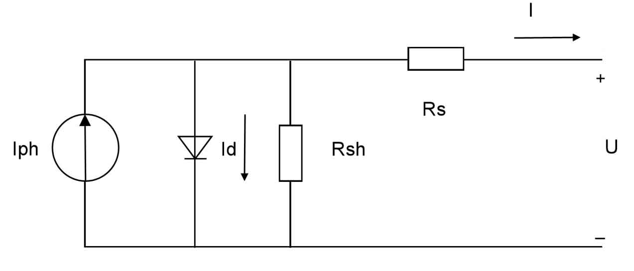
If the directions indicated by the arrows in Figure 1 are all positive, the I-U characteristic equation of the solar cell can be obtained from the circuit in the figure:
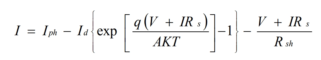
Among them: I is the battery output current (A); V is the output voltage (V); Iph is the photogenerated current (A); Id is the reverse saturation current of the diode (A); Q is the amount of charge (1.6 × 10⁻¹⁹C); K is the Boltzmann constant (1.38 × 10⁻²³J/K); T is the absolute temperature of the solar cell (T=t+237K); A is the diode quality factor (1 when the forward bias voltage is high and 2 when it is low); Rs is the series resistance (low resistance value) of the battery; Rsh is the parallel resistance (high resistance value) of the battery. The relationship between I-V can be obtained from formula 1, which is the electrical characteristic of the solar cell, i.e. the I-V output characteristic. From this, the I-V characteristic curve can be obtained, as shown in Figure 2.
As shown in Figure 2, solar cells are a nonlinear DC power source, where Im is the maximum operating point current and Vm is the maximum operating point voltage. When V=0, i.e. when the battery circuit is short circuited, there is a short-circuit current Isc; The voltage when the corresponding circuit is open is Voc in the figure.
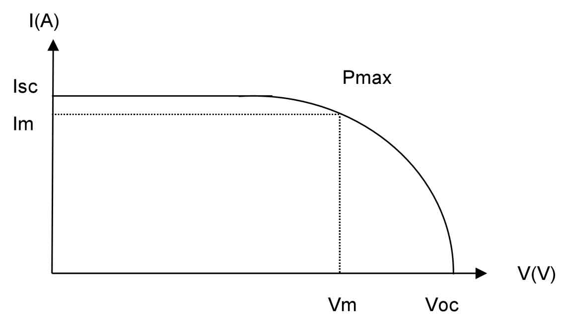
By using the power calculation formula P=UI, the P-U output characteristic curve of the solar cell can be obtained. As shown in Figure 3:
From Figure 3, it can be intuitively seen that the relationship between voltage and power of solar cells is one-to-one, so under certain external environmental conditions, the maximum power point of solar cells is unique. When the actual operating point of the solar cell is to the left of the maximum power point, as the output voltage increases, the output power also increases; When the actual working point is on the right side of the maximum power point, as the output voltage continues to increase, the power begins to decrease from maximum to 0.
In practical applications, solar cells are not only affected by their own volt ampere characteristics, but also by temperature T (℃) and light intensity (W/㎡).
3. DC/DC conversion circuit
The DC/DC conversion circuit, together with the inverter circuit, serves as a direct bridge between the photovoltaic cell and the public grid. Its function is to convert the lower voltage level DC energy output by the solar photovoltaic cell into higher voltage level DC voltage energy, and then allow that level of DC energy to output grid connected AC energy through the inverter.
3.1 Classification of DC/DC conversion circuits
DC/DC conversion circuits mainly include buck, boost, and buck boost circuits.
1) Buck converter
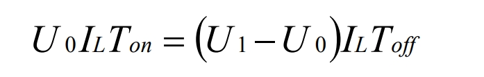
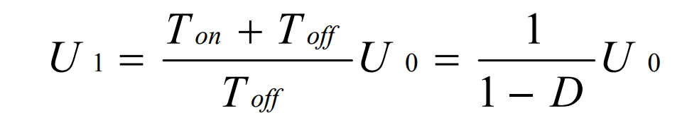
The circuit diagram of the Buck conversion circuit is shown in Figure 4. This circuit uses a fully controlled device V, which is shown in the figure as an IGBT. Other devices can also be used. The output voltage of the Buck converter circuit is less than or equal to the input voltage, and the relationship between the two can be more intuitively seen through formula 2 provided in the following text. So it is a step-down chopper circuit. The working principle of Buck converter: When the switch V is closed, the diode is in the reverse cut-off state, and the load is powered by the photovoltaic power supply. The IL of the current flowing through the inductor continues to increase, and the inductor and capacitor are in the charging state. When switch V is turned off, the diode is in a conductive state and the capacitor begins to discharge. Due to the freewheeling effect of the inductor, the current will slowly decrease. This is the general workflow of the Buck circuit.
After analyzing the workflow of the Buck circuit shown in the above figure, it can be concluded that:
In the formula, D represents the duty cycle of the Buck transformed circuit, Ts is the switching cycle of the switching transistor V, and Ton is the turn-on time.
The Buck converter circuit in a solar grid connected system adds an additional parallel capacitor compared to traditional Buck circuits. This is because if there is a lack of parallel capacitors as an energy storage element in the solar grid connected system, there may be interruptions during operation. When the diode in the circuit is turned off, the capacitor enters a charging state, making full use of solar energy. But this will increase the volume of that part of the device.
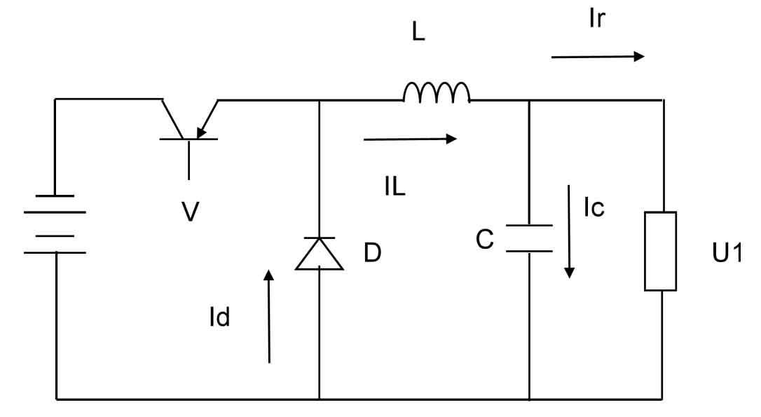
2) Boost converter circuit
The circuit diagram of the Boost transformation circuit is shown in Figure 5:
The Boost converter circuit is a boost chopper circuit, so its output voltage is greater than the input voltage. This relationship can also be intuitively seen from formula 4 derived in the following text. In this circuit, it can be seen that there is a diode connected in series on its main circuit, which has an anti backflow effect here, effectively preventing the electrical energy from the grid from feedback to the photovoltaic array.
The working principle of the Boost circuit: When the switching tube V is conducting, it is obvious that diode D is short circuited. At this time, the inductor receives charging from the power supply, while the capacitor is in a discharge state; When the switching tube V is turned off, the inductor begins to discharge, and at this time, the inductor and the photovoltaic power supply discharge together, and the capacitor is in a charging state.
By combining the circuit diagram and working principle, it can be concluded that:
Organized:
From equation 4, it can be seen that the output to input voltage ratio of the Boost converter circuit is always greater than 1, which is why it is used as a boost chopper circuit.
3) Buck Boost converter circuit
Based on the knowledge introduced earlier, it can be inferred that this transformation circuit is capable of both making its output voltage higher than the input voltage and its output voltage lower than the input voltage. The circuit is shown in Figure 6:
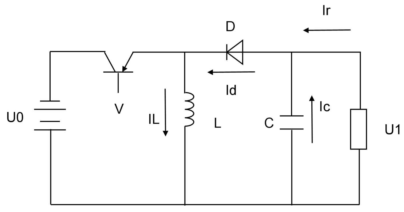
As shown in the figure, when the switching tube V is closed, diode D is in the off state. At this time, the power supply charges the inductor L, the capacitor is in the discharge state, and supplies power to the load. When the switching tube V is disconnected, diode D conducts and inductor L is in a discharge state, providing energy to the load.
From the circuit diagram and working principle, it can be concluded that:
Obviously, for the variable D in the equation, when D=0.5, U0=U1; When D<0.5, U1>U0, the transformation circuit plays a role in reducing voltage; When D>0.5 and U1<U0, the transformation circuit plays a boosting role. So compared to the previous two circuits, the Buck boost circuit has more complete functions and wider applications.
3.2 Selection of DC/DC conversion circuit
Three main DC/DC converters were introduced and analyzed. Through analysis, it is found that the household solar grid connected power generation system studied in this paper is more suitable to choose a Boost converter for composition. Because in household solar power generation systems, the DC voltage level converted by solar cells is generally relatively low, requiring a boost converter circuit to raise it to a higher voltage level. Compared to another buck boost circuit that can boost, the Boost converter circuit has a relatively simple structure and is more convenient to operate. So the DC/DC converter is selected as the Boost converter circuit.
4. Photovoltaic grid connected inverters
Inverters, which are electrical devices that can convert direct current into alternating current, are the core components of solar grid connected power generation systems. The solar power generation system is regarded as an active inverter system, and the main task of photovoltaic grid connected inverters is to convert the direct current generated by the photovoltaic array, which is converted from absorbed solar energy, into alternating current with the same frequency and phase as the grid. It can not only provide electricity to the load but also integrate the electricity into the grid. So the characteristics and control methods of grid connected inverters determine the quality of the AC power they input into the grid, which is an irreplaceable part of the power generation system.
4.1 Working principle of inverter
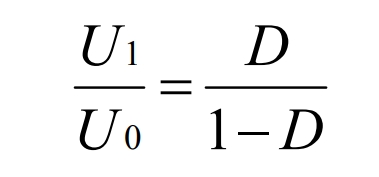
Inverters are generally composed of DC filtering, boost circuit, and inverter bridge circuit. After filtering the DC voltage output by the DC/DC converter circuit, the DC voltage is first boosted by a boost circuit, and then converted into AC voltage at power frequency through an inverter bridge circuit. This is the rough process of inverter operation. Inverters are mainly composed of switching elements such as transistors, which convert DC input into AC output with waveform. However, this simple transformation of the AC waveform does not meet the requirements for grid connection. It is necessary to perform high-frequency pulse width modulation (SPWM) on the waveform to form a waveform that is close to a sine wave. Finally, a simple filtering device is used to obtain the sine wave.
The simple structure diagram of the grid connected inverter is shown in Figure 7:
The functions of each part in the diagram are consistent with those described above, and the relay section at the end is also an indispensable protective device in the circuit. Its function is to ensure the normal operation of the inverter circuit and avoid damage to components in the circuit.
4.2 Classification of grid connected inverters
There are many different standards for classifying the main circuit structure of inverters, such as dividing them into active or passive inverters based on the direction of AC energy; It can be divided into unidirectional or bidirectional inverters based on the direction of power supply; It can also be directly divided into half bridge, full bridge, and push-pull inverters based on the structure of the main circuit. Here, we will discuss the classification of inverter isolation methods.
Inverters are mainly divided into the following categories based on isolation methods:
1) Power frequency isolation
2) High frequency link isolation
3) Transformer free method
Below is a brief introduction to the various methods mentioned above:
1) Power frequency isolated inverter: In the design process of the inverter, the main isolation device used is the transformer. So in the power frequency isolated inverter, the isolation device used is the power frequency transformer. Using a power frequency transformer for isolation and insulation while achieving voltage transformation can effectively eliminate sharp waves in inverter circuits. Additionally, there are few semiconductor devices used in the circuit, making it very simple, efficient, and adaptable.
2) High frequency isolated inverter: As mentioned in the introduction of the previous inverter, the isolation insulation device is mainly a transformer, which is also used for transformer insulation. However, this circuit undergoes multi-level transformation, so the structure of the circuit is more complex and the working efficiency is lower than that of the previous form of inverter. Although this circuit has efficiency issues, it can also be corrected by selecting appropriate electrical components.
3) Transformer free mode: Transformer free mode inverters are currently the mainstream in photovoltaic grid connected inverters. It consists of an inverter circuit and a boost circuit, among which the boost circuit will be discussed and selected in subsequent chapters. Thanks to the boost circuit, the input voltage of the inverter is ensured to be more stable while reducing losses.
Based on the above, although the circuit of the transformer free method is slightly more complex than that of the power frequency transformer method, its performance, work efficiency, stability, and other aspects have been significantly improved, making it the most suitable photovoltaic power generation system for this research topic.
5. Overall Plan of the System
Based on the discussion and research in each previous section of this chapter, the existing solutions for selecting the main components of the solar grid connected power generation system are as follows:
In terms of grid connected inverters, this project adopts a transformer free inverter structure, which, together with the DC/DC conversion circuit, forms two stages before and after. And for the DC/DC conversion circuit, after comparison in the previous text, a relatively simple Boost boost circuit was selected. In terms of control circuit, the DSP control chip TMS320LF2407A is selected to ensure the grid connection conditions of the inverter output power.
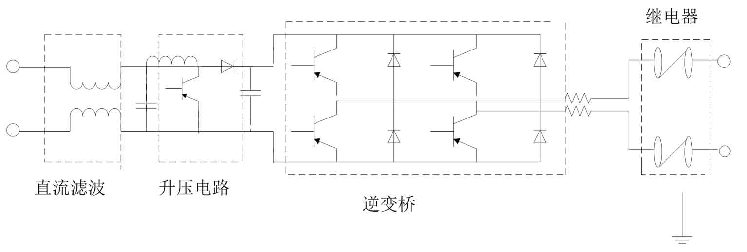
The main circuit of the system is shown in Figure 8:
The circuit consists of a solar panel, a DC/DC conversion circuit, and an inverter circuit. The leftmost electrical component is the solar panel, and the specific parameters of each main electrical component in the circuit will be calculated based on the power requirements set in this project.